Formation of silicon nanocrystals in sapphire by ion implantation
and the origin of visible photoluminescence
S. Yerci,a兲U. Serincan, and I. Dogan
Department of Physics, Middle East Technical University, 06531 Ankara, Turkey S. Tokay
Department of Physics, Kirikkale University, 71450 Kirikkale, Turkey M. Genisel
Department of Chemistry, Middle East Technical University, 06531 Ankara, Turkey A. Aydinli
Department of Physics, Bilkent University, 06531 Ankara, Turkey R. Turan
Department of Physics, Middle East Technical University, 06531 Ankara, Turkey
共Received 17 March 2006; accepted 6 July 2006; published online 4 October 2006兲
Silicon nanocrystals, average sizes ranging between 3 and 7 nm, were formed in sapphire matrix by ion implantation and subsequent annealing. Evolution of the nanocrystals was detected by Raman spectroscopy and x-ray diffraction共XRD兲. Raman spectra display that clusters in the matrix start to form nanocrystalline structures at annealing temperatures as low as 800 ° C in samples with high dose Si implantation. The onset temperature of crystallization increases with decreasing dose. Raman spectroscopy and XRD reveal gradual transformation of Si clusters into crystalline form. Visible photoluminescence band appears following implantation and its intensity increases with subsequent annealing process. While the center of the peak does not shift, the intensity of the peak decreases with increasing dose. The origin of the observed photoluminescence is discussed in terms of radiation induced defects in the sapphire matrix. © 2006 American Institute of Physics. 关DOI:10.1063/1.2355543兴
I. INTRODUCTION
Observation of intense photoluminescence 共PL兲 from nanocrystalline silicon1and its charge storing capabilities has attracted much attention because of its potential applications in optoelectronic2,3 and charge storing devices.4 Silicon nanocrystal embedded in SiO2 共Si-nc/SiO2兲 structures have been widely studied for both applications. Nevertheless, the origin of the PL from Si-nc/ SiO2 structures is still contro-versial. It has been proposed to originate from the quantum confinement of carriers in Si nanocrystals,5,6 surface states such as SivO bonds formed on the surface of the nanocrystals,7 and defects in the oxide.8 SiO2 films on Si substrate are widely used for charge storage for it has supe-rior electrical properties and it can be easily grown thermally on Si substrates. On the other hand, shrinking dimensions of gate dielectrics led researchers to look for alternative mate-rials having similar insulating properties as SiO2 but with higher dielectric constant than SiO2. Al2O3 is a promising candidate for gate oxide material because its dielectric con-stant is twice as much as that of SiO2 and the band gap of Al2O3 共9.2 eV兲 is very similar to that of SiO2 共8.7 eV兲.9 Furthermore, semiconductor nanocrystals in Al2O3 matrix can be considered as a suitable structure for optical device
applications due to optical transparency of Al2O3. The pro-duction of nonvolatile memory devices containing nanocrys-tals in high-k oxides, such as alumina, has been studied extensively.10 Thin films of Al2O3 can be grown on Si sub-strate by using present well-developed integrated circuit pro-cesses. The reverse is also true. Si-nc can be formed in Al2O3 matrix with various methods such as pulsed laser deposition,9 cosputtering,11 electron beam coevaporation,12 electrochemistry,13 and ion implantation.14–16 Among these methods, ion implantation is of particular interest because of its compatibility with the existing complementary metal-oxide semiconductor 共CMOS兲 technology and its superior control over the position and dose of the ions, therefore of nanocrystals.
In this study, silicon nanocrystals were formed in
␣-Al2O3 matrix by ion implantation and followed by an an-nealing process in the temperature range of 600– 1100 ° C. Evolution of nanocrystal formation and their optical emis-sion properties have been investigated by XRD, Raman, and PL spectroscopies as a function of the implanted Si dose and annealing temperature. XRD was employed to calculate the size of the nanocrystals. Moreover, systematic correlation be-tween the Raman signals of varying doses and annealing parameters was used to track the amorphous to crystalline phase changes and the deviation of stress on nanocrystals. Finally, detailed PL measurements were performed to search for the origin of the emission mechanism.
a兲Author to whom correspondence should be addressed; electronic mail: [email protected]
II. EXPERIMENT
C-plane oriented ␣-Al2O3 substrates were implanted with 100 keV 28Si+ ions at doses of 1⫻1016, 1⫻1017, and 2⫻1017Si/ cm2 and annealed at 600, 700, 800, 900, and 1100 ° C in N2ambient for 2 h to induce Si nanocrystal for-mation. The projected range 共Rp兲 of the Si ions was calcu-lated as 81 nm usingTRIMsoftware.17All PL measurements were conducted at room temperature with the 488 nm line of an Ar+ laser, operated at 300 mW. The emitted light was detected with a photomultiplier tube. Raman measurements were employed in backscattering geometry at room tempera-ture using 632.8 nm as light source of a confocal micro-Raman 共HR800, Jobin Yvon兲, attached with Olympus mi-croanalysis system and a charge-coupled device 共CDD兲 camera providing a resolution of ⬃1 cm−1. XRD measure-ments were conducted with a standard x-ray powder diffrac-tometer, using Cu K␣ radiation. Conventional Bragg-Brentano ⌰–2⌰ scans were employed with scans between 5° and 80° at 0.02° steps. Acquisition time per angular steps of 24 s was used to enhance the signal to noise ratio. The data used were the average of three scans. The full width at half maximum共FWHM兲 of the diffraction peak 共0.122°兲 of a standard sample of microcrystalline powder Si was recorded to eliminate the instrumental line broadening. The Si 共111兲 peak at 28.4° was used for both the correction of the instru-mental broadening and the calculation of the nanocrystal sizes.
III. RESULTS AND DISCUSSION A. X-ray diffraction„XRD…
The XRD signals corresponding to Si 共111兲, with 2⌰ value around 28.6°, became evident at annealing tempera-tures of 900 and 1000 ° C for the samples implanted with doses of 2⫻1017 and 1⫻1017 Si/ cm2, respectively. Mea-sured spectra from samples annealed at 900, 1000, and 1100 ° C with the dose of 2⫻1017 Si/ cm2 as well as those annealed at 1000 and 1100 ° C with the dose of 1 ⫻1017Si/ cm2 are displayed in Fig. 1. The formation of
Si-nc having 共111兲 direction has been extensively studied in other matrices such as SiO2 using XRD.18,19Moreover, the same structure was studied in sapphire matrix with electron diffraction.14,15As shown in the inset of Fig. 1, Si共111兲 XRD signal broadens with decreasing annealing temperatures en-abling us to calculate the average grain sizes of nanocrystals and their evolution with the annealing temperature. Size cal-culation using XRD is simple and nondestructive which pro-vides an average value for the nanocrystals size. The average nanocrystal size determination was performed using Scher-rer’s formula, which agrees well with other experimental techniques such as high-resolution transmission electron mi-croscopy共HRTEM兲, when uncertainties for all are taken into account.19Scherrer’s formula is given as
D = k
cos⌰,
where D is the average grain size,  is the FWHM of the diffraction peak after the elimination of instrumental line broadening,is the Bragg angle, is the wavelength of the x ray共0.154 nm兲, and k=0.89 is the Scherrer constant. The residual Cu K␣2 was corrected by using the Rachinger cor-rection method which assumes the intensity of the K␣2 as half as that of K␣1.20 The background correction was per-formed assuming quadratic polynomial background which gives the best fit. Figure 2 displays the data and the subse-quent fit to the XRD signal from the sample implanted with 2⫻1017 Si cm−2 and annealed at 1100 ° C. Peak profiles were assumed to be pseudo-Voigt, which is a combination of Gaussian and Cauchy line shapes.
Following Scherrer’s formula, average nanocrystal sizes are estimated to be 7.2± 0.2 and 5.1± 0.2 in samples im-planted with the dose of 2⫻1017Si/ cm2 and subsequently annealed at 1100 and 1000 ° C, respectively. Similarly, in samples implanted with the dose of 1⫻1017Si/ cm2, average Si nanocrystal sizes are found to be 7.0± 0.2 and 3.9± 0.2 nm for annealing temperatures of 1100 and 1000 ° C, respec-tively. These values of nanocrystal sizes are in good agree-ment with the reported values as determined from HRTEM analysis.16The uncertainties given in D values are statistical errors associated with the determination of the FWHM of Si 共111兲 Bragg peak only. While stress may induce additional FIG. 1. The evolution of XRD signal of Si implanted␣-Al2O3matrix as a
function of implantation dose and annealing temperature.共*兲 indicates the Si共111兲 peaks. Inset shows details of Si 共111兲 peaks.
FIG. 2. Si共111兲 XRD peak at 28.6°. The solid line is a fit to data using a pseudo-Voigt function.
broadening, it is difficult to deconvolute the effect of finite size and stress from the FWHM of the diffraction peak. Ten-sile or compressive stress will also cause a shift in the Bragg diffraction peak position from its bulk counterpart which can be used to evaluate the magnitude and direction of stress. We, therefore, used the position of the diffraction peak posi-tion to evaluate stress from the XRD data.
The measured lattice constant for the nanocrystals is al-ways smaller than the lattice constant of 5.43 Å obtained from the reference sample of polycrystalline Si, for all doses of implantation and temperatures of annealing, which im-plies compressive stress on nanocrystals with the mean lat-tice compression of ⌬a/a=0.04% –0.11%. This result can be explained with the lattice mismatch between the nano-crystals and the host matrix. A reasonable explanation for this stress requires a careful examination of the phase trans-formations of both the nanocrystals and the host matrix dur-ing the ion implantation and annealdur-ing process. While the nanocrystals formed at lower annealing temperatures 共800–900 °C兲 are mostly amorphous they crystallize after annealing at around 1100 ° C.21For the surrounding matrix, although no phase formation of Al2O3 other than ␣-Al2O3 was observed in XRD measurements, the creation of ⌰-Al2O3 was previously reported after annealing of amor-phized Al2O3 matrix by ion implantation with the dose of 5⫻1016Si/ cm2.14⌰-Al
2O3has a monoclinic structure with lattice constants of a = 11.79 Å, b = 2.91 Å, and c = 5.62 Å. The minimum lattice mismatch is about 3.4% which can be responsible from the compressive stress. On the other hand,
␣-Al2O3 is the most stable phase among the Al2O3 phases which is formed after 1000– 1100 ° C annealing. ␣-Al2O3 has a hexagonal structure with the lattice constants of 4.758 and 12.991 Å. Therefore, in the present case, minimum lat-tice mismatch can be calculated as 14% between the nano-crystals and the host matrix. This mismatch should generate large amounts of mechanical stress on Si nanocrystals.
B. Raman spectroscopy
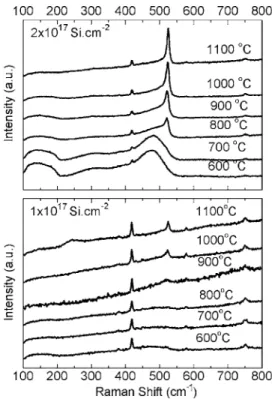
Raman spectra of as-implanted samples are given in Fig. 3. The peaks at around 418, 577, and 750 cm−1are from the crystalline host matrix. The intensity of these peaks de-creases with increasing doses because of partial
amophiza-tion of the matrix. While no Raman signals for Si–Si bonds were observed from the sample with the dose of 2 ⫻1016Si/ cm2, Raman signals typical for amorphous Si were detected in the sample with doses of 1⫻1017 and 2 ⫻1017Si/ cm2.22
The bands recorded from higher dose im-planted samples are described as transverse acoustic 共TA兲 band around 150 cm−1, transverse optical共TO兲 band around 480 cm−1, and mixed acoustic-optical band around 310 cm−1. One could safely conclude that implantation with the dose of 2⫻1016 Si/ cm2 is not sufficient to generate amorphous Si clusters detectable with Raman spectroscopy 共Fig. 3兲 and XRD. Annealing at 1100 °C did not yield any Si nanocrystal formation in this sample either. The atomic per-centage Si concentration for this fluence at peak position of the Si distribution is estimated to be 2.6% withTRIMcodes.17 Raman spectroscopy clearly demonstrates the formation and the evolution of Si nanocrystals in the Al2O3matrix as a function of annealing temperature, as shown in Fig. 4. The evolution of the Si–Si bonds, which shows the transforma-tion from the amorphous phase to crystalline phase, can be observed from the variation of the Raman peaks seen at 150, 310, and 480 cm−1 with the annealing temperature 共Fig. 4兲. The bands measured at 150 and 310 cm−1 from the samples with high dose implantation diminish with increasing anneal-ing temperatures and disappear almost completely after 1100 ° C for 2 h annealing. We see that amorphous Si clus-ters formed in the as-implanted samples transform into crys-talline Si structures with a more intense and narrow Raman signal as the annealing temperature increases. As is also ob-served by XRD, both the size and the number of Si nano-crystals increase with the increasing annealing temperature and the dose. The evolution of the TO band of Si nanocrys-tals is commonly considered as an indicator of crystallinity FIG. 3. Raman spectra of ␣-Al2O3 implanted with doses of 2⫻1016, 1
⫻1017, and 2⫻1017Si/ cm2.
FIG. 4. The evolution of Raman signal for the doses of 1⫻1017 and 2 ⫻1017Si/ cm2implanted samples with annealing temperature.
in Si structures. While amorphous Si has a broad TO band around 480 cm−1, bulk Si has a sharp TO band with a natural linewidth of approximately 3 cm−1around 521 cm−1at room temperature. Moreover, it is known that this band for nano-crystalline Si shows a broadening and a shift to lower wave numbers due to the phonon confinement effect.23A qualita-tive comparison of the Raman signals measured for different doses and annealing temperatures indicates that while the nanocrystal formation starts at 800 ° C for the sample with a dose of 2⫻1017Si/ cm2, it begins at around 900 ° C for the sample with a dose of 1⫻1017Si/ cm2.
It was reported that the compressive stress can cause a shift to higher wave numbers, acting in the opposite direction to the phonon confinement effect.21The competition between the two mechanisms determines the position of the peak. Therefore, the methods, developed for the size estimation of the Si nanocrystals by using the shift and the broadening of Si TO Raman signals, are questionable in the case of large stress as in the present case.24,25Calculation of the size and the stress requires a separation between both parts from the Raman shift. The magnitude of the stress can be estimated from the stress induced wave number shift,⌬s:
26
共MPa兲 ⬇ 250⌬s共cm−1兲,
whereis the magnitude of the stress and⌬sis the stress induced wave number shift. In this calculation, the Raman shift due to the phonon confinement effect was first consid-ered using results established by Campell and Fauchet, who calculated the relationship between the Raman shift and the size of the unstressed spherical nanocrystals using Gaussian a weighting function.24 Following to this calculation, the stress induced wave number shifts were found by subtracting these values from the corresponding experimental wave number values. The approximate magnitudes of the stress were calculated as 2.57, 1.73, and 1.71 GPa in samples im-planted with the dose of 2⫻1017Si/ cm2 and subsequently annealed at 900, 1100, and 1000 ° C, respectively. Similarly, those values were calculated as 2.20 and 1.66 GPa in samples with the dose of 1⫻1017 Si/ cm2for annealing tem-peratures of 1000 and 1100 ° C, respectively. It seems that the amount of stress is larger on the smaller nanocrystals formed at lower temperatures and it reaches almost a con-stant value when the nanocrystal formation process is com-pleted.
C. Photoluminescence
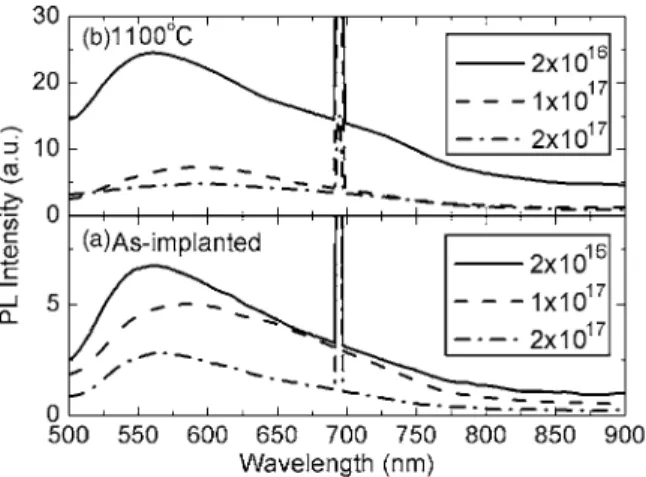
PL spectra of Si implanted Al2O3matrix exhibit mainly three peaks in the visible region. Of these, the emission at around 694 nm is due to PL from Cr3+ impurities in the matrix15 and the emission at around 740 nm may due to Ti3+.27,28
The latter peak also exists in the case of Ar+, Al−, and O− implanted Al
2O3.15,28 However, as reported by others,13–15 the PL band seen at 570 nm appears after ion implantation followed by subsequent annealing and both its intensity and position may vary with increasing annealing temperatures. The origin of this emission is controversial. The discussions are mainly focused on three mechanisms; size dependent light emission from Si nanocrystals,14,15
emission from Si clusters or from very small nanocrystals,28 and emission from matrix defects, mainly F center related defects.13
The PL spectra 关Fig. 5共a兲兴 of the as-implanted samples with varying doses display three PL bands at around 570 nm, 694 nm, and a shoulder around 710 nm. The latter two bands are assigned to Cr3+and Ti3+impurities, respectively. Having no indication of Si nanocrystal formation from the XRD and Raman measurements, the PL signal seen at 570 nm in the as-implanted samples is thought to be due to F22+ 共two oxy-gen vacancies with two trapped electrons兲,29–31
introduced into the Al2O3matrix during ion implantation. The intensity of the PL band at 570 nm in the as-implanted samples de-creases with the implantation dose, indicating that the lumi-nescent centers created by the ion implantation are quenched by additional implantation.32 This decrease may result from the annihilation of the luminescence centers due to either destruction of the light emitting structures formed by Si im-plantation at low doses or formation of new nonradiative centers which dominates the transitions. Contrary to the dose effect, high temperature annealing at 1100 ° C results in an enhancement of the PL peak for all implantation doses. The variation is highest for the lowest dose of 2⫻1016Si/ cm2. However, neither amorphous nor crystalline Raman features were observed from implanted samples with this dose. Fur-thermore, no clear shift was observed in PL spectra during phase transformation of the clusters from amorphous to crys-tal structures observed with Raman spectroscopy. The quan-tum confinement model suggests a redshift with nanocrystal size. Lack of shift in the PL spectra indicates that the ob-served light emission is not related to the excitonic transi-tions that take place in the core of the nanocrystals. This is further supported by the fact that the PL signal diminishes with increased dose for which the nanocrystal formation is clearly monitored by Raman spectroscopy and XRD 共Figs. 1–4兲. The origin of the PL signal at 570 nm may be con-nected to point defects such as F22+ centers formed in the matrix by ion implantation. The lack of PL signal from the nanocrystals may be a result of large stress on nanocrystals as evidenced by Raman spectroscopy. The stress can break the bonds at the interface and be responsible for the creation of nonradiative centers around the nanocrystals. Another FIG. 5. PL spectra of共a兲 as implanted and 共b兲 1100 °C annealed samples of varying doses.
speculation might be the lack of SivO bonds which are believed to be responsible for the light emission from Si nanocrystals formed in SiO2 matrix.33
IV. CONCLUSIONS
The formation of Si nanocrystals in Al2O3matrix by ion implantation and subsequent annealing is studied with Ra-man spectroscopy, XRD, and PL spectroscopy. The nano-crystal sizes are obtained from the width of Si 共111兲 XRD pattern by applying Scherrer’s formula. In agreement with the expectations from the lattice mismatch between Si nano-crystals and the host matrix, large amount of compressive stress is estimated from the analysis of the Raman signal. Since the as-implanted samples possess similar emission fea-tures and center of the band does not shift during the forma-tion of nanocrystals, the origin of the PL band around 570 nm was considered as defect related. The corresponding defect is assumed as an F22+ center. The reason for the ab-sence of nanocrystal related PL may be due to the extraordi-nary compressive stress on Si nanocrystals or the lack of SivO bonds in Si-nc/Al2O3structures.
ACKNOWLEDGMENTS
This work has been partially supported by the European Commission through the FP6 project called SEMINANO un-der Contract No. NMP4-CT-2004-505285. The authors thank Professor E. Bulur for the helpful discussion on the F center defects.
1L. T. Canham, Appl. Phys. Lett. 57, 1046共1990兲.
2K. D. Hirschman, L. Tsybeskov, S. P. Duttagupta, and P. M. Fauchet, Nature共London兲 384, 338 共1997兲.
3U. Serincan, G. Aygun, and R. Turan, J. Lumin. 113, 229共2005兲. 4Z. Lu, J. Shen, B. Mereu, M. Alexe, R. Scholz, V. Talalaev, and M.
Zacharias, Appl. Phys. A: Mater. Sci. Process. 80, 1631共2005兲. 5V. Lehman, and U. Gosele, Appl. Phys. Lett. 61, 1948共1991兲. 6X. Y. Chen, Y. F. Lu, L. J. Tang, Y. H. Wu, B. J. Cho, X. J. Xu, J. R. Dong,
and W. D. Song, J. Appl. Phys. 97, 014913共2005兲.
7L. Khriachtchev, O. Kilpela, S. Karirinne, J. Keranen, and T. Lepisto,
Appl. Phys. Lett. 78, 323共2001兲.
8M. Prokes, Appl. Phys. Lett. 62, 3244共1993兲.
9Y. Zhu, H. Wang, and P. P. Ong, J. Phys. D 33, 2687共2000兲.
10T. Baron, A. Fernandes, J. F. Damiencourt, B. De Salvo, F. Martin, F. Mazen, and S. Haukka, Appl. Phys. Lett. 82, 4151共2003兲.
11L. Bi and J. Y. Feng, J. Lumin. 121, 95共2006兲.
12Q. Wan, N. L. Zhang, X. Y. Xie, T. H. Wang, and C. L. Lin, Appl. Surf. Sci. 191, 171共2002兲.
13M. Kokonou, A. G. Nassiopoulou, and A. Travlos, Mater. Sci. Eng., B 101, 65共2003兲.
14S. Yanagiya and M. Ishida, J. Electron. Mater. 28, 498共1999兲. 15C. J. Park, Y. H. Kwon, Y. H. Lee, T. W. Kang, H. Y. Cho, S. Kim, S. H.
Choi, and R. G. Elliman, Appl. Phys. Lett. 84, 2667共2004兲.
16D. I. Tetelbaum, A. N. Mikhaylov, O. N. Gorshkov, A. P. Kasatkin, A. I. Belov, D. M. Gaponova, and S. V. Morozov, Vacuum 78, 519共2005兲. 17J. F. Ziegler, J. P. Biersack, and U. Littmark, The Stopping and Range of
Ions in Solids共Pergamon, New York, 1985兲.
18M. Morales, Y. Leconte, R. Rizk, and D. Chateigner, J. Appl. Phys. 97, 034307共2004兲.
19D. Comedi, O. H. Y. Zalloum, E. A. Irving, J. Wojcik, T. Roschuk, M. J. Flynn, and P. Mascher, J. Appl. Phys. 99, 023518共2006兲.
20H. P. Klug and L. E. Alexander, X-Ray Diffration Procedures共Wiley, New York, 1974兲.
21G. Viera, S. Huet, and L. Boufendi, J. Appl. Phys. 90, 4175共2001兲. 22T. Zheng and Z. Li, Superlattices Microstruct. 37, 227共2005兲.
23D. Nesheva, C. Raptis, A. Peraklis, I. Bineva, Z. Aneva, Z. Levi, S. Al-exandrova, and H. Hofmeister, J. Appl. Phys. 92, 4678共2002兲. 24I. H. Campbell and P. M. Fauchet, Solid State Commun. 58, 739共1986兲. 25Ch. Ossadnik, S. Veprek, and I. Gregora, Thin Solid Films 337, 148
共1999兲.
26J. Marcia, E. Martin, A. Perez-Rodriquez, J. Jimenez, J. M. Morante, B. Aspar, and J. Margial, J. Appl. Phys. 82, 3730共1997兲.
27L. E. Bausa, I. Vergara, F. Jaque, and J. Garcia Sole, J. Phys.: Condens. Matter 2, 9919共1990兲.
28D. I. Tetelbaum, O. N. Gorshkov, A. V. Ershov, A. P. Kasatkin, V. A. Kamin, A. N. Mikhaylov, A. I. Belov, D. M. Gaponova, L. Pavesi, L. Ferraioli, T. G. Finstad, and S. Foss, Thin Solid Films 515, 333共2006兲. 29Y. Song, C. H. Zhang, Z. G. Wang, Y. M. Sun, J. L. Duan, and Z. M. Zhao,
Nucl. Instrum. Methods Phys. Res. B 245, 210共2006兲.
30T. Mohanty, N. C. Mishra, F. Singh, S. V. Bhat, and D. Kanjilal, Radiat. Meas. 36, 723共2003兲.
31T. Mohanty, N. C. Mishra, F. Singh, U. Tiwari, and D. Kanjilal, Nucl. Instrum. Methods Phys. Res. B 212, 179共2003兲.
32K. S. Jheeta, D. C. Jain, F. Singh, R. Kumar, and K. B. Garg, Nucl. Instrum. Methods Phys. Res. B 224, 187共2006兲.
33L. Khriachtchev, M. Rasanen, S. Novikov, and L. Pavesi, Appl. Phys. Lett. 85, 1511共2004兲.