REDUCING PROCESSOR-MEMORY
PERFORMANCE GAP AND IMPROVING
NETWORK-ON-CHIP THROUGHPUT
a dissertation submitted to
the graduate school of engineering and science
of bi̇lkent university
in partial fulfillment of the requirements for
the degree of
doctor of philosophy
in
computer engineering
By
Naveed Ul Mustafa
February 2019
REDUCING PROCESSOR-MEMORY PERFORMANCE GAP AND IMPROVING NETWORK-ON-CHIP THROUGHPUT
By Naveed Ul Mustafa February 2019
We certify that we have read this dissertation and that in our opinion it is fully adequate, in scope and in quality, as a dissertation for the degree of Doctor of Philosophy.
Özcan Öztürk(Advisor)
Süleyman Tosun
Uğur Güdükbay
Muhammet Mustafa Özdal
Kayhan Mustafa İmre
Approved for the Graduate School of Engineering and Science:
Ezhan Karaşan
ABSTRACT
REDUCING PROCESSOR-MEMORY PERFORMANCE
GAP AND IMPROVING NETWORK-ON-CHIP
THROUGHPUT
Naveed Ul Mustafa Ph.D. in Computer EngineeringAdvisor: Özcan Öztürk February 2019
Performance of computing systems has tremendously improved over last few decades primarily due to decreasing transistor size and increasing clock rate. Billions of transistors placed on a single chip and switching at high clock rate result in overheating of the chip. The demand for performance improvement without increasing the heat dissipation lead to the inception of multi/many core design where multiple cores and/or memories communicate through a network on chip. Unfortunately, performance of memory devices has not improved at the same rate as that of processors and hence become a performance bottleneck. On the other hand, varying traffic pattern in real applications limits the network throughput delivered by a routing algorithm.
In this thesis, we address the issue of reducing processor-memory performance gap in two ways: First, by integrating improved and newly developed memory technologies in memory hierarchy of a computing system. Second, by equip-ping the execution platform with necessary architectural features and enabling its compiler to parallelize memory access instructions. We also address issue of improving network throughput by proposing a selection scheme that switches routing algorithm of an NoC with changing traffic pattern of an application.
We present integration of emerging non-volatile memory (NVM) devices in memory hierarchy of a computing system in the context of database manage-ment systems (DBMS). To this end, we propose modifications in storage engine (SE) of a DBMS aiming at fast access to data through bypassing the slow disk interfaces while maintaining all the functionalities of a robust DBMS. As a case study, we modify the SE of PostgreSQL and detail the necessary changes and challenges such modifications entail. We evaluate our proposal using a compre-hensive emulation platform. Results indicate that our modified SE reduces query
iv
execution time by up to 45% and 13% when compared to disk and NVM stor-age, with average reductions of 19% and 4%, respectively. Detailed analysis of these results shows that our modified SE suffers from data readiness problem. To solve this, we develop a general purpose library that employs helper threads to prefetch data from NVM hardware via a simple application program interface (API). Our library further improves query execution time for our modified SE when compared to disk and NVM storage by up to 54% and 17%, with average reductions of 23% and 8%, respectively.
As a second way to reduce processor-memory performance gap, we propose a compiler optimization aiming at reduction of memory bound stalls. The pro-posed optimization generates efficient instruction schedule through classification of memory references and consists of two steps: affinity analysis and affinity-aware instruction scheduling. We suggest two different approaches for affinity analysis, i.e., source code annotation and automated analysis. Our experimental results show that application of annotation-based approach on a memory intensive pro-gram reduces stall cycles by 67.44%, leading to 25.61% improvement in execution time. We also evaluate automated-analysis approach using eleven different im-age processing benchmarks. Experimental results show that automated-analysis reduces stall cycles, on average, by 69.83%. As all benchmarks are both compute and memory-intensive, we achieve improvement in execution time by up to 30%, with a modest average of 5.79%.
In order to improve network throughput, we propose a selection scheme that switches routing algorithm with changing traffic pattern. We use two selection strategies: static and dynamic selection. While static selection is made off-line, dynamic approach uses run-time information on network congestion for selection of routing algorithm. Experimental results show that our proposal improves throughput for real applications up to 37.49%.
They key conclusion of this thesis is that improvement in performance of a computing system needs multifaceted approach i.e., improving the performance of memory and communication subsystem at the same time. The reduction in performance gap between processors and memories requires not only integration of improved memory technologies in system but also software/compiler support. We also conclude that switching routing algorithm with changing traffic pattern of an application leads to improvement of NoC throughput.
v
Keywords: Memory bound stalls, compiler optimization, execution time,
com-puter vision, non volatile memory, relational DBMS, storage engine, network-on-chip, routing algorithm, throughput.
ÖZET
İŞLEMCİ-BELLEK PERFORMANS FARKINI
AZALTMAK VE YONGA ÜSTÜ AĞ VERİMİNİ
ARTIRMAK
Naveed Ul MustafaBilgisayar Mühendisliği, Doktora Tez Danışmanı: Özcan Öztürk
Şubat 2019
Bilişim sistemlerinin performansı son yıllarda, özellikle transistör boyutunun azal-ması ve saat hızının artazal-ması nedeniyle muazzam bir gelişme göstermiştir. Tek bir yonganın üzerine yerleştirilmiş milyarlarca transistör ve yüksek saat hızında anahtarlama, yonganın aşırı ısınmasına neden olmaktadır. Isı dağılımını artır-madan performans iyileştirme gereksinimi, çoklu çekirdeklerin ve/veya belleklerin yonga üzerindeki bir ağ üzerinden iletişim kurduğu çoklu çekirdek tasarımlarının kullanılmasına yol açmıştır. Ne yazık ki, bellek performansı, işlemci performansı ile aynı hızda gelişememiştir ve bu nedenle bellekler bir performans darboğazı haline gelmiştir. Diğer yandan, gerçek uygulamalarda değişen trafik düzenleri, bir rotalama algoritması tarafından gözetilen ağ verimliliğini kısıtlamaktadır.
Bu tezde, işlemci-bellek performans farkı sorununu iki şekilde ele alıyoruz: Bir-incisi, gelişmiş ve yeni geliştirilen bellek teknolojilerini bir bilgisayar sisteminin bellek hiyerarşisinde birleştiriyoruz. İkincisi, yürütme platformunu gerekli mi-mari özelliklerle donatıyor ve derleyicinin bellek erişim talimatlarını paralel hale getirmesini sağlıyoruz. Ayrıca, bir Yonga üzeri Ağ (YüA)’nın rotalama algorit-masını, bir uygulamanın değişen trafik düzenine göre değiştiren bir seçim yöntemi önererek, ağ verimliliğinin kısıtlanması sorununu da ele alıyoruz.
Yeni gelişen kalıcı bellek (Non-volatile memory - NVM) cihazlarının bir bil-gisayar sisteminin bellek hiyerarşisinde, veri tabanı yönetim sistemleri (DBMS) bağlamında entegrasyonunu sunuyoruz. Bu amaçla, bir DBMS’nin depolama motorunda (SE), DBMS’nin fonksiyonlarının doğru çalışmasını etkilemeden, disk arayüzlerini atlayarak verilere hızlı erişim sağlayan değişiklikler öneriyoruz. Bir uygulama çalışması olarak, PostgreSQL’in SE’sini değiştiriyoruz ve bu değişik-liğin gereksinimlerini ve zorlukları detaylandırıyoruz. Önerdiğimiz yaklaşımı kapsamlı bir emülasyon platformu kullanarak değerlendiriyoruz. Sonuçlar, disk ve NVM deposuyla karşılaştırıldığında, değiştirilmiş SE’mizin sorgu sürelerini
vii
sırasıyla %19 ve %4’lük bir ortalama azalışla, %45 ve %13’e kadar azalttığını göstermektedir. Bu sonuçların detaylı analizi, değiştirilmiş SE’mizin veri hazır-lığı sorununa tâbi olduğunu göstermektedir. Bu sorunu çözmek için, basit bir uygulama programı arayüzü (API) yoluyla NVM donanımından belleğe önce-den veri almak için yardımcı iş parçacıkları kullanan genel amaçlı bir kütüphane geliştirdik. Bu kütüphanemiz ile, değiştirilmiş SE için disk ve NVM depolamaya kıyasla sorgu sürelerinin sırasıyla ortalama %23 ve %8’lik bir düşüşle, %54 ve %17’ye kadar azaltılabildiği görülmüştür.
İşlemci bellek performansı farkını azaltmak üzere ikinci bir yol olarak, belleğe bağlı duraklamaların azaltılmasını amaçlayan bir derleyici optimizasyonu öneriy-oruz. Önerilen optimizasyon, bellek referanslarının sınıflandırılması yoluyla etk-ili bir sıralama oluşturmaktadır ve iki adımdan oluşmaktadır: ilginlik analizi ve ilginlik duyarlı sıralama. İlginlik analizi için iki farklı yaklaşımı öneriyoruz; kaynak kod ek açıklaması ve otomatik analiz. Deneysel sonuçlarımız, ek açık-lama tabanlı yaklaşımın uygulanmasının, bellek erişimi yoğun bir programda du-raklama döngülerini %67,44 azaltarak çalışma süresinde %25,61 kadar iyileşme sağladığını göstermektedir. Ayrıca 11 farklı görüntü işleme değerlendirme deneyi ile otomatik analiz yaklaşımımızı değerlendirdik. Deneysel sonuçlar, otomatik analizin duraklama döngülerini ortalama %69,83 oranında azalttığını göstermek-tedir. Tüm deneylerde hem hesaplama hem de bellek yoğun işlemler olduğu için, çalışma süresinde ortalama %5.79 iyileşme olmakla birlikte bu oran %30’a kadar çıkmaktadır.
Ağ verimliliğini arttırmak için, rotalama algoritmasını değişen trafik düzenine göre değiştiren bir seçim yöntemi öneriyoruz. İki seçim stratejisi kullanıyoruz: statik ve dinamik seçim. Statik seçim devre dışı bırakıldığında, dinamik yak-laşım, rotalama algoritmasının seçimi için ağ tıkanıklığına ilişkin koşum zamanı bilgilerini kullanmaktadır. Deneysel sonuçlar, yöntemimizin gerçek uygulamalar için %37,49’a kadar verimliliği artırdığını göstermektedir.
Bu tezin temel sonucu, bir bilgisayar sisteminin performansında iyileşme elde etmek için çok yönlü bir yaklaşıma ihtiyaç duyulduğudur, yani aynı anda hem bellek, hem de iletişim alt sisteminin performansının iyileştirilmesi gerektiğidir. İşlemciler ve bellekler arasındaki performans farkının azaltılması için yalnızca gelişmiş bellek teknolojilerinin sisteme entegrasyonu değil, aynı zamanda yazılım/ derleyici desteği de gerekmektedir. Ayrıca, bir uygulamanın değişen trafik düze-nine göre rotalama algoritmasının değiştirilmesinin, YüA veriminin artmasını sağladığı sonucuna varılmıştır.
viii
Anahtar sözcükler: Belleğe bağlı duraklama, derleyici optimizasyonu, yürütme
süresi, bilgisayar görüntüleme, kalıcı bellek, ilişkisel veritabanı, depolama motoru, yonga üstü ağ, yönlendirme algoritması, verim.
ix
I dedicate this work to my MOTHER & FATHER who always supported me at every stage of my life. I can never payback their love and affection.
Acknowledgement
My six and a half year journey of PhD studies at Bilkent University was a pleasant learning experience. It helped me to deepen my knowledge of computer science and gain research experience. It would have not been possible to write this PhD thesis without support of many people. Therefore, I would like to avail this opportunity to pay my deep gratitude to them. First and foremost, I am grateful to Allah Almighty who gave me the opportunity for PhD studies, helped me stay strong and gave me the consistency needed for completion of PhD.
I would like to extend my sincere thanks to my supervisor, Dr. Özcan Özturk, for his excellent supervision and all necessary support needed during PhD studies. Whether it was about adopting a specific strategy for solving a research problem or selection of a simulation platform for evaluation of a proposal, discussions with him and his feedback was always very helpful and time saving. I thank Özcan for enabling me to have collaboration with researchers at Barcelona Supercomputing Center (BSC) and introducing me to HiPEAC community leading to another collaborative research project with Movidius-Intel.
I am also very thankful to Dr. M. Mustafa Özdal who gave me an opportunity to work on Graph Processor project. Although still in progress, the project intro-duced me to area of graph processors, their challenges and simulation platforms to model potential solution to those challenges.
I am grateful to the members of my thesis committee: Dr. Buğra Gedik, Dr. M. Mustafa Özdal from Bilkent University, Dr. Suleyman Tosun and Dr. Kayhan İmre from Hacettepe University for their valuable comments and discussions. I also show gratitude to my colleagues at Özyeğin University, Dr. Hasan Sözer and Dr. Kübra Kalkan Çakmakçı, for Turkish translation of the abstract.
I would also like to thank Martin J.O'Riordan and Stephen Rogers from Movidius-Intel, Dr. Adrià Armejach, Dr. Adrián Cristal and Dr. Osman Sabri Ünsal from BSC for collaboration and support needed for implementation of re-search ideas reported in this thesis. I would like to acknowledge Dr. Smail Niar from Université Polytechnique Hauts-De-France (UPHF) for his supervision and helpful feedback in a collaborative research on network-on-chip. He was more than only a research supervisor as his talks were a source of encouragement in
xi
facing ups and downs of life during my PhD studies.
My lab mates were also an important part of PhD studies as they contributed towards this thesis in different ways, sometime providing their feedback on im-proving the draft of a research article, helping in learning a tool, listening to problems of life and learning the Turkish language. I would like to thank Hamzeh Ahangari, Can Fahrettin Koyuncu, Şerif Yeşil, Mohammad Reza Soltaniyeh, Simge Gökçe, Tolga and Gülden for being my wonderful labmates.
I would also like to thank my friends without whom life at Bilkent would have been so boring and dull. Thanks to Ali Haider, Umar Raza, Muhammad Waqas Akbar, Muhammad Sabih Iqbal, Naveed Mehmood, Talha Masood, Abdur Rahman Dandia, Salahudin Zafar, Ali Shiraz, Asad Ali, Abdullah and Zulfiqar for filling my years at Bilkent with colors and fun.
The support I got in form of encouragement, prayers and love from my par-ents, Muhammad Zawar and Khadim Noor, is unforgettable as they were always there when I needed them. It is due to their prayers that I have successfully ful-filled requirements for PhD. I would also like to thank my beautiful and beloved daughter Eman Azad, my sisters Azra, Saeeda, Hameedah, Misbah, Zeenat and my brother Zia Ul Mustafa Danish for providing me the warmth of the family.
I would like to express my deep thanks to Merve Naveed Ul Mustafa for being a source of support and strength in my last three years at Bilkent, first as my fiancée and then as my wife.
Lastly, I express a deep sense of gratitude to Higher Education Commission (HEC) of Pakistan for financially supporting my PhD.
Contents
1 Introduction 1 1.1 Research Problem . . . 5 1.2 Motivation . . . 7 1.3 Thesis Statement . . . 9 1.4 Contributions . . . 10 1.5 Outline . . . 12 2 Background 13 2.1 Memory Hierarchy of a DBMS . . . 14 2.2 Characteristics of NVM . . . 152.3 Prior Work on Usage of NVM in DBMS Design . . . 17
2.4 Computer Vision: Applications and Platforms . . . 18
2.5 Myriad 2 Architecture . . . 20
2.5.1 CMX Memory . . . 21
2.6 Prior Work on Reduction of Memory Bound Stalls . . . 22
2.7 Network-on-Chip Routing . . . 25
2.7.1 Prior Work on Reconfiguring Noc Routing Algorithm . . . 26
3 Integrating NVM in Memory Hierarchy of a DBMS 28 3.1 Memory Hierarchy Designs for an NVM-Based DBMS . . . 29
3.2 System software for NVM . . . 30
3.3 Potential Modifications in a Traditional DBMS . . . 31
3.4 Discussion . . . 32
3.5 A Case Study: PostgreSQL . . . 33
CONTENTS xiii
3.5.2 SE1: Using Memory Mapped I/O . . . 35
3.5.3 SE2: Direct Access to Mapped Files . . . 36
3.6 Data Consistency and Modified Storage Engines . . . 37
3.7 Software Library for NVM Data Prefetching . . . 38
3.7.1 Helper Threads . . . 39
3.7.2 Library Services . . . 39
3.7.3 Thread Mapping Schemes . . . 40
4 Compiler Optimization for Reduction of Memory Bound Stalls 44 4.1 Limitations of a Generic Compiler . . . 44
4.2 Proposed Solution . . . 45
4.2.1 Source Code Annotation . . . 52
4.2.2 Automated Analysis . . . 53
4.2.3 Discussion . . . 55
4.3 Implementation . . . 56
4.3.1 Affinity Analysis Through Source Code Annotation . . . . 56
4.3.2 Affinity Analysis Through Automated Analysis . . . 57
4.3.3 Affinity-Aware Instruction Scheduling (AAIS) . . . 58
5 A Selection Scheme for NoC Routing Algorithms 59 5.1 Routing Algorithms . . . 59
5.2 Traffic Patterns . . . 61
5.2.1 Effect of Traffic Patterns on Performance of Routing Algorithms . . . 62
5.3 Static Selection . . . 62
5.4 Dynamic Selection . . . 63
6 Evaluation 66 6.1 Evaluation of NVM-Aware Storage Engines: SE1 and SE2 . . . . 66
6.1.1 Methodology . . . 67
6.1.2 Workloads . . . 68
6.1.3 Performance Evaluation of SE1 and SE2 . . . 70
CONTENTS xiv
6.1.5 Performance Evaluation of SE2 Coupled With Data
Prefetching Library . . . 75
6.2 Evaluation of Compiler Optimization . . . 79
6.2.1 Experimental Setup . . . 80
6.2.2 Experimental Results for Source Code Annotation . . . . 82
6.2.3 Experimental Results for Automated Affinity Analysis . . 87
6.3 Evaluation of Selection Scheme for NoC Routing Algorithm . . . 89
6.3.1 Simulator and Benchmarks . . . 90
6.3.2 Experimental Results for SPARSE . . . 90
6.3.3 Experimental Results for MPEG-4 Decoder . . . 93
6.3.4 Experimental Results for H264-720p . . . 95
6.3.5 Experimental Results for FPPPP . . . 97
7 Conclusion 99
List of Figures
1.1 Increasing clock speed and number of transistors per chip. . . 2 1.2 Increasing power consumption on a 100mm2 die. . . . 2
1.3 Increasing number of cores in Intel's Xeon processors. . . 3 1.4 Nine cores connected through (a) a P2P (b) a bus architecture (c)
and a 3x3 mesh, an example of NoC. . . 4 1.5 Increasing performance (speed) gap between microprocessors and
memory. . . 4 1.6 Execution time breakdown for benchmarks: P1 = Subtraction of
two images, P2 = Addition of four images, P3 = Addition of two images, P4 = Addition of two images based on a mask input, P5 = Box filtering using 5x5 mask, P6 = Addition of two scaled images, P7 = Convolution using 3x3 mask, P8 = Sum of abso-lute difference using a 5x5 window, P9 = White balancing oper-ation, P10=Histogram generoper-ation, P11=Similarity measurement between pixels of two images. . . 6 1.7 Network throughput for H.264 video decoder with a resolution of
720p. . . 9 2.1 Architectural layout of a Myriad 2 platform. . . 20 2.2 Organization of the CMX memory and its interface with SHAVE
processors in Myriad 2. Memory is divided into slices (a) and each slice is divided into regions (b). . . 21 2.3 16 PEs connected through a 4x4 mesh NoC. . . 26 3.1 NVM placement in the memory hierarchy of a DBMS. . . 29
LIST OF FIGURES xvi
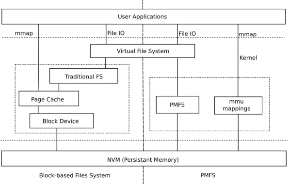
3.2 Comparison of traditional FS and PMFS. “mmap” refers to the system call for memory mapped I/O operation. “mmu” is the memory management unit responsible for address mappings. . . . 31 3.3 High level view of read and write memory operations in
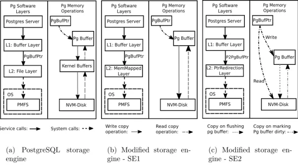
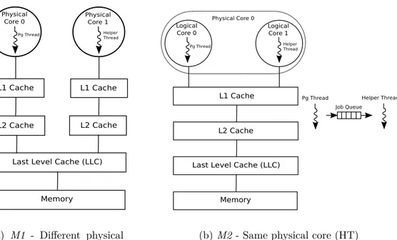
Post-greSQL (read as “pg” in short form) and modified SEs. . . 34 3.4 Thread mapping schemes for a single helper thread with and
with-out hyper-threading (HT) enabled. . . 42 3.5 Thread mapping scheme for two helper threads. . . 43 4.1 Different scenarios where two memory objects belong to different
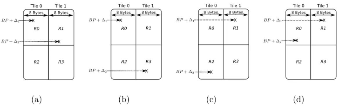
tiles. BP + ∆ is the address of a memory object, where BP is the base address and ∆ is the offset from BP . . . . 47 4.2 Different scenarios where two memory objects belong to the same
tile. Figure 4.2(a) shows that absolute difference Dif f between offsets of two memory objects is greater than or equal to 64K bytes, indicating that two memory objects belong to different regions. Figure 4.2(b) shows Dif f less than 64K bytes and memory objects belong to different regions. Figure 4.2(c) and 4.2(d) show Dif f less than 64K bytes but memory objects belong to the same region. 48 4.3 Predictions of physical locations through source code annotation. 53 4.4 Implementation of automated analysis as a custom pass in LLVM.
Address analysis pass (AAP) appends affinity numbers to memory objects using Algorithm 1. Modified SHAVE PostRAS pass creates affinity-aware instruction schedule based on affinity numbers. . . . 58 5.1 XY Routing algorithm first routes data packets from source to
destination along (a) X direction and then along (b) Y direction. 60 5.2 Routing of data packets through (a) west-first (b) north-last and
(c) negative-first algorithms. Red colored links are congested ones while green color indicates taken path. . . 61 5.3 An NxN mesh: congestion level at a router is a measure of
LIST OF FIGURES xvii
6.1 Execution time breakdown for TPCH queries in traditional DBMS with database stored in disk-storage. . . 69 6.2 Percentage of kernel execution time for each query. . . 70 6.3 Wall-clock execution time normalized with respect to pmfs_base95. 71 6.4 Execution-time breakdown for compute and stalled cycles — B =
pmfs_base95, SE2 = pmfs_se2. . . . 73
6.5 Last-level cache (LLC) misses breakdown — B = pmfs_base95, SE2 = pmfs_se2. . . . 73 6.6 Percentage of kernel execution time for PostgreSQL thread. . . . 75 6.7 Wall-clock execution time normalized with respect to pmfs_base95. 76 6.8 Execution time breakdown into compute and stall cycles for
Post-greSQL thread, normalized with respect to pmfs_base95. . . 77 6.9 L1 cache misses for PostgreSQL thread normalized with respect
to pmfs base95. . . 77 6.10 Execution time breakdown into compute and stall cycles for helper
thread running on same physical core as PostgreSQL in M2 and M3. Execution time is normalized with respect to M2. . . 79 6.11 Instruction schedule generated by BC for Listing 6.1. . . 82 6.12 Instruction schedule generated by AAC for Listing 6.2. . . 86 6.13 Breakdown of execution time into instruction and stall cycles for
executions using BC and AAC. . . 88 6.14 Breakdown of simultaneous memory access into three different
cases. Case A: Memory objects belong to different tiles. Case
B: Memory object belong to the same tile but different regions. Case B_2: Memory objects belong to the same region of the same
tile. . . 88 6.15 Number of received packets in the case of XY and west-first
rout-ings for SPARSE application. . . 91 6.16 Number of received packets in the case of static and dynamic
se-lection between XY and west-first routings for SPARSE application. 92 6.17 Number of received packets in the case of west-first and
LIST OF FIGURES xviii
6.18 Number of received packets in the case of static and dynamic se-lection between west-first and negative-first routings for MPEG-4 decoder application. . . 94 6.19 Network throughput in the case of west-first and north-last
rout-ings for H264-720p application. . . 96 6.20 Network throughput in the case of static and dynamic selection of
routing algorithms for H264-720p application. . . 96 6.21 Network throughput in the case of west-first and north-last
rout-ings for FPPPP application. . . 98 6.22 Network throughput in the case of static and dynamic selection of
List of Tables
1.1 Comparison of different NVM technology with SSD and HDD. . . 7
2.1 Comparison of architectural features of different CV platforms (read DNA as “Details not available”). . . 25
4.1 Comparison of AAIS with BIS in Case B. . . . 49
6.1 Test machine characteristics. . . 68
6.2 Brief description of benchmarks. . . 81
6.3 Throughput comparison for SPARSE application. . . 93
Chapter 1
Introduction
A computer, by definition, is an entity performing computation [1]. Computers are omnipresent and the driving force of the information age we are living in not only because they compute but also because they store data and perform communication [2]. Like humans, computers are also on a journey of progress from the start of their history. They are expected to provide an ever increasing higher performance since the announcement of first digital computer, ENIAC, in year 1946 [3, 4].
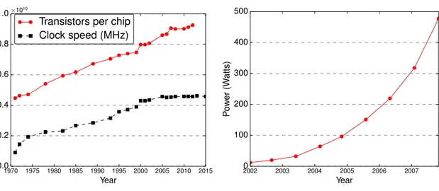
Performance of a computing system is determined by the individual perfor-mance of all three of its major components: processor, memory and a commu-nication architecture. Performance of a processor can be characterized in terms of rate at which it performs a given task [5]. Based on this definition, clock rate of a processor is a commonly used performance metric [6]. As shown in Figure 1.1 (reproduced from [7]), clock rate has increased over the years. Coupled with improving instructions per cycle (IPC), increasing clock rate made it possible for processors to achieve performance improvement [8]. At the same time, shrinking transistor size allowed placement of more number of transistors on a single chip [9] (See Figure 1.1), making it possible to perform more logic.
1970 1975 1980 1985 1990 1995 2000 2005 2010 2015 Year 0.0 0.2 0.4 0.6 0.8 1.0×10¹⁰
Transistors per chip Clock speed (MHz)
Figure 1.1: Increasing clock speed and number of transistors per chip.
2002 2003 2004 2005 2006 2007 Year 0 100 200 300 400 500 Po w er (W atts)
Figure 1.2: Increasing power con-sumption on a 100mm2 die.
frequency result in prohibitively large power consumption, as shown in Figure 1.2 (reproduced from [10]), placing a limit on further increasing the clock rate [11, 12]. As a way to circumvent the power limit and still improve the performance of a processor, researchers proposed to keep frequency increase at a minimum and use multiple simpler cores on a single chip [13, 14].
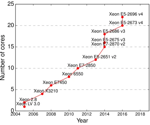
Multi-core processors exhibit performance gain over a comparable single core processor [15], and hence widely adopted in domains such as image processing [16, 17], embedded systems [18, 19, 20], big data analytics [21], signal processing [22, 23] , and computer vision [24, 25] among others. The wide scale adoption of multi-core platforms is reflected by growing number of cores on a single chip such as intel's Xeon processors, shown in Figure 1.3.
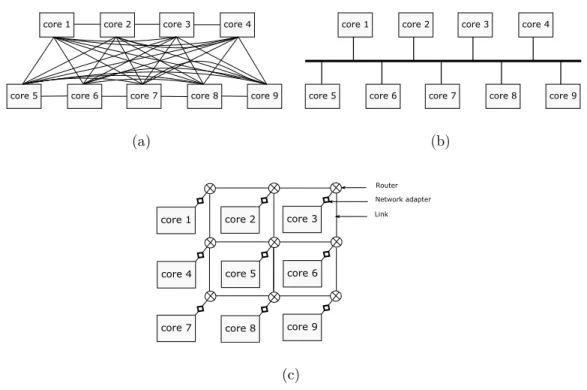
A multi-core design necessitates an on-chip communication architecture to connect multiple cores with each other and/or with memories. Traditionally, point-to-point (P2P) and bus communication architectures have been used for on-chip communication. However, P2P architecture suffers from lack of scala-bility in terms of complexity and cost (Figure 1.4(a)). On the other hand, bus architecture is simpler than P2P communication (Figure 1.4(b)) but it also lacks scalability and suffers from limited bandwidth [26]. As a result, P2P or bus archi-tectures can not meet the communication needs of multi/many-core era, making
2004 2006 2008 2010 2012 2014 2016 2018 Year 0 5 10 15 20 25
Number
of
cores
Xeon LV 3.0Xeon 2.8 Xeon X3210 Xeon E7450 Xeon 6550 Xeon E7-2850 Xeon E5-2651 v2 Xeon E7-2870 v2 Xeon E5-2675 v3 Xeon E5-2686 v3 Xeon E5-2673 v4 Xeon E5-2696 v4Figure 1.3: Increasing number of cores in Intel's Xeon processors. the communication a performance bottleneck [27].
Network-on-chip (NoC) has emerged as a viable alternative, serving as com-munication backbone for many-core based system-on-chip (SoC) designs [28]. An NoC connects processing and storage resources via a scalable network [26] (Figure 1.4(c)) and promises efficient communication between multiple cores, caches, and memory controllers [29].
Processors retrieve data from repositories known as memories. Therefore, per-formance of computing systems is determined not only by processors and commu-nication architecture but also by memory subsystem. Unfortunately, performance of memory devices has not improved at the same rate as that of processors. There is an increasing performance gap between processors and memories as shown in Figure 1.5 (reproduced from [30]). As a result, for many applications, not pro-cessors but the limited bandwidth and long access latency of memory proves to be a serious performance bottleneck [31].
core 1 core 2 core 3 core 4
core 5 core 6 core 7 core 8 core 9
(a)
core 1 core 2 core 3 core 4
core 5 core 6 core 7 core 8 core 9
(b) core 1 Router Network adapter Link core 4 core 7 core 2 core 5 core 8 core 3 core 6 core 9 (c)
Figure 1.4: Nine cores connected through (a) a P2P (b) a bus architecture (c) and a 3x3 mesh, an example of NoC.
1985 1990 1995 2000 2005 2010 Year 100 101 102 103 104 105 Perf or mance Microprocessor performance Memory performance
Figure 1.5: Increasing performance (speed) gap between microprocessors and memory.
1.1
Research Problem
Execution time of an application can be divided into two broad categories: com-mit cycles and stall cycles. A clock cycle is categorized as a comcom-mit cycle if at least one instruction is retired during the cycle; otherwise, it is categorized as a stall cycle. Various reasons such as unavailability of functional units, bad branch prediction, or data dependencies result in stall cycles. The unavailability of data required for instruction execution incurs extra clock cycles. Such cycles are termed as memory bound stalls (MBS).
In order to highlight performance bottlenecks of a computing system, we ana-lyze the execution time of a set of compute and memory-intensive benchmarks se-lected from computer vision domain. Benchmarks perform basic image-processing operations such as image addition and subtraction [32], box filtering [33], con-volution [34], sum of absolute difference [35], white balancing operation [36], histogram generation, and similarity measurement between pixels of two input images [37]. Appendix A provides the critical part of the source code for bench-marks.
We use Intel’s VTune performance analyzer [38] to breakdown the execution time of benchmarks into commit cycles (CC), bad speculation stalls (BSS), MBS, core bound stalls (CBS), and front-end bound stalls (FEBS). MBS originate from performance gap between processors and memories. Number of MBS depends on level of memory hierarchy holding the required data. Lower the data resides in memory hierarchy, higher is the number of MBS. As shown in Figure 1.6, on average, MBS make almost 33% of the total execution time. In other words, 33% of an application's execution time is spent waiting for data arrival from memory subsystem. It suggests that performance gap between processors
and memory subsystem is a performance bottleneck.
In a multi-core platform, data transportation between cores and/or memories is performed by an NoC. A routing algorithm determines path of data transport [39] and hence significantly impacts the NoC latency and throughput [40]. Many
P1 P2 P3 P4 P5 P6 P7 P8 P9 P10 P11 Avg 0 20 40 60 80 100 120 Ex ecution Time (%) CC BSS MBS CBS FEBS
Figure 1.6: Execution time breakdown for benchmarks: P1 = Subtraction of two images, P2 = Addition of four images, P3 = Addition of two images, P4 = Addition of two images based on a mask input, P5 = Box filtering using 5x5 mask, P6 = Addition of two scaled images, P7 = Convolution using 3x3 mask, P8 = Sum of absolute difference using a 5x5 window, P9 = White balancing operation, P10=Histogram generation, P11=Similarity measurement between pixels of two images.
algorithms have been proposed for on-chip routing [41, 42, 43, 44].
Performance of a routing algorithm is affected by traffic pattern which rep-resents the distribution of messages in an NoC [45]. Traffic pattern of a real application is determined by communication links between its tasks mapped on different cores. A source task may have communication links to one or multiple destination tasks i.e. spatial distribution of traffic. Also, tasks may inject data at different time points and at different rates (i.e temporal distribution of traffic). As a result, traffic patterns of real applications are non-uniform and may vary over time.
Deterministic algorithms, such as XY [41], always route data along the same path for a given pair of source and destination. Since traffic pattern of real appli-cations is non-uniform, XY outing is not a good fit for them. Partially adaptive algorithms, such as west-first and north-last [42], allow multiple paths for a source and destination pair. However, performance of such algorithms is affected by traf-fic pattern. For example, if most of traftraf-fic flows leftward in a particular interval of the application's execution period then west-first routing algorithm reduces
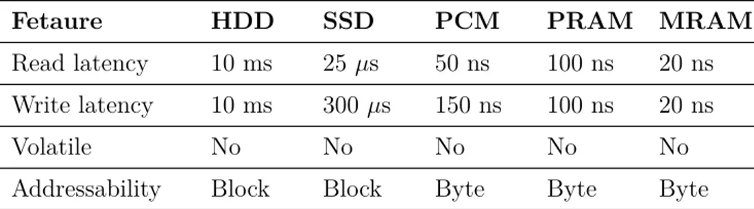
Table 1.1: Comparison of different NVM technology with SSD and HDD.
Fetaure HDD SSD PCM PRAM MRAM
Read latency 10 ms 25 µs 50 ns 100 ns 20 ns
Write latency 10 ms 300 µs 150 ns 100 ns 20 ns
Volatile No No No No No
Addressability Block Block Byte Byte Byte
throughput in that interval. In other words, applying a single routing
algo-rithm for whole execution period of a real application (with changing traffic pattern) becomes a bottleneck for throughput improvement.
1.2
Motivation
As an effort to reduce performance gap between processors and memories (shown in Figure 1.5), computing systems use a memory hierarchy organized into several levels and take the advantage of principle of locality in accessing data [46]. A storage device, such as hard disk drive (HDD) or solid state disk (SSD), sits at the lowest level of this hierarchy offering features of non-volatility, highest capacity, lowest cost but longest access latency.
Non volatile memory (NVM) is an emerging storage class technology. Like disk storage, it provides feature of non-volatility (or persistency) but with much lower access latency than SSD/HDD technologies, as shown in Table 1.1. It also supports data access at byte-level granularity [47]. Due to its promising features, NVM has been investigated for use in computing systems as an on-chip cache[48], main memory and storage device [47, 49].
We believe that features of NVM can be exploited to reduce per-formance gap between processors and memory subsystem of an I/O-intensive computing systems. An example of I/O-I/O-intensive computing system
solutions used to facilitate complex decision making [50] and convert business information into tangible results [51] to help executives take knowledge-based decisions. DSS frequently read huge data sets from system storage.
A database management system (DBMS) is a necessary component of DSS. In a traditional DBMS, HDD is used to provide means of durable storage. However, reads and write operations to an HDD are very expensive. Performance of mem-ory subsystem (including storage device) can be improved by avoiding expensive I/O operations through replacement of HDD/SSD with an NVM storage device. Another way to reduce performance gap between processors and memories is to reduce MBS by parallelizing multiple memory accesses. The parallelization requires architectural support not only at the level of memory subsystem (for example, multi-port and multi-bank memories) but also at core-level (for example, multiple load-store units). However, architectural innovations without proper software support are not sufficient. Compilers need to generate efficient
instruction schedule by considering architectural features for reduction of MBS.
Performance of a computing system is also affected by its communication ar-chitecture. For example, higher NoC latency or lower throughput increases the travel time of data from memories to processors and hence result in higher num-ber of MBS. A routing algorithm significantly impacts NoC throughput. At the same time, performance of an algorithm is affected by traffic pattern. To high-light effect of an application's changing traffic pattern on network throughput delivered by a routing algorithm, we analyze performance of west-first and north-last algorithms. We simulate a real application i.e., H.264 video decoder with a resolution of 720p.
Variations in the network throughput delivered by west-first and north-last routing algorithms, as shown in Figure 1.7, can be interpreted in two complemen-tary ways. First, varying traffic pattern of an application affects the throughput of routing algorithms. Second, network-throughput can be improved by
10000 20000 30000 40000 50000 60000 70000 80000 90000 100000 Time(Cycles) 0.08 0.10 0.12 0.14 0.16 0.18 Throughput north-last west-first
Figure 1.7: Network throughput for H.264 video decoder with a resolution of 720p.
traffic pattern of an application. For example, network throughput in case of
H.264 video decoder application can be improved if there is a mechanism to apply west-first routing in simulation interval of 10K to 48K cycles and than switch to north-last routing in simulation interval of 48K to 100K cycles.
1.3
Thesis Statement
Our thesis statement is:
1. Performance gap between processors and memories of a computing system can be reduced by integrating improved and newly developed memory tech-nologies in its memory hierarchy.
2. MBS can be reduced by parallelizing memory accesses through an optimized architecture-aware compiler.
appropriate routing algorithms with changing traffic pattern of real appli-cations.
1.4
Contributions
In this thesis we mainly contribute by proposing solutions to improve performance of memory subsystem and NoC. More specifically, this thesis makes following main contributions.
1. We discuss and provide insights on different available options when includ-ing NVM into the memory hierarchy of computinclud-ing systems for reducinclud-ing performance gap between processor and memory subsystem. We address the problem in the context of DBMS. We focus on investigating the neces-sary changes and challenges when modifying an existing, well-tested, widely used, and robust traditional DBMS to benefit from NVM features. As a case study, we select PostgreSQL which is ranked as the 4th most popular DBMS [52].
We propose modification in the storage engine (SE) of a DBMS aiming at providing fast access to data by bypassing the slow disk interfaces while maintaining all the functionalities of a robust DBMS such as PostgreSQL. We evaluate our proposed modification in SE of PostgreSQL using a com-prehensive emulation platform. We identify and quantify performance bot-tlenecks that appear when employing NVM hardware. To further improve the performance of our NVM-enabled SEs, we design and implement a gen-eral purpose data prefetching library based on helper threads that tackles the identified performance bottlenecks.
We evaluate our modified SE by running TPC-H benchmark [53]. Evalua-tion results indicate that modified SE (without usage of prefetching library) reduces query execution time by up to 45% and 13% when compared to disk and NVM storage, with average reductions of 19% and 4%, respectively. Modified SE coupled with data prefetching library further improves query
execution time when compared to disk and NVM storage by up to 54% and 17%, with average reductions of 23% and 8%, respectively. This work is presented in SAMOS 2016 conference and published in its proceedings [54]. 2. We propose a compiler optimization aiming at reduction of MBS through classification of memory references. The optimization consists of two steps: affinity analysis and afnity-aware instruction scheduling (AAIS). While affinity analysis predicts the physical memory location for each memory object in the application’s source code, AAIS generates a stall-saving in-struction schedule based on the results of affinity analysis step. We propose two different affinity analysis approaches, namely, source code annotation and automated analysis. We present implementation of the proposed opti-mization on LLVM compiler infrastructure.
We evaluate annotation-based approach on a memory-intensive program achieving a reduction in stall cycles by 67.44%, leading to 25.61% improve-ment in execution time. We also use 11 different image-processing bench-marks for evaluation of automated analysis approach. Our experimental results show that proposed optimization reduces stall cycles, on average, by 69.83%. As all benchmarks used for evaluation of automated analysis approach are both compute and memory-intensive, we achieve improve-ments in execution time by up to 30%, with a modest average of 5.79%. This work is published in JRTIP [55].
3. We propose a selection scheme to improve throughput of an NoC by se-lecting appropriate routing algorithms with changes in the traffic pattern of an application. We aim at selecting a routing algorithm which delivers higher throughput for traffic pattern constituted by active communication flows in each interval, and hence improve the overall network throughput for execution period. We propose two different approaches for algorithm selection: static selection and dynamic selection. We evaluate our proposal by executing different benchmarks on NoCs of different sizes. Experimental results show that our proposal improves throughput by up to 37.49%. This work is published in proceedings of RAPIDO 2016 workshop [56].
1.5
Outline
Thesis is organized into 7 Chapters. Chapter 2 provides necessary background on proposed techniques for reducing processor-memory performance gap and im-proving NoC throughput. It also presents a brief survey of prior related work. Chapter 3 elaborates on integration of NVM in memory hierarchy of a DBMS. Chapter 4 explains the compiler optimization for reduction of MBS. Chapter 5 presents the selection scheme for routing algorithms in order to improve network throughput. Chapter 6 provides the detailed experimental evaluation of our pro-posed techniques. Chapter 7 concludes the thesis while Appendix A provides supplementary data.
Chapter 2
Background
This chapter is organized into three parts. In the first part, consisting of Section 2.1 to 2.3, we describe DBMS from memory hierarchy perspective, explain prop-erties of NVM technologies, highlight the implications these features might have in the design of a DBMS and describe prior related work on usage of NVM in DBMS design.
In the second part, consisting of Section 2.4 to 2.6, we present a brief introduc-tion of computer vision applicaintroduc-tions and the architecture of execuintroduc-tion platform used for evaluation of the proposed compiler optimization (detailed in Chapter 4). We also present a brief survey of prior related work on reduction of MBS and compare it with the proposed compiler optimization.
In the third part, consisting of Section 2.7 and 2.7.1, we discuss NoC routing algorithms, traffic patterns and their effect on algorithm performance along with a brief survey of prior work on reconfiguring NoC routing algorithm.
2.1
Memory Hierarchy of a DBMS
The traditional design of a DBMS assumes a memory hierarchy where datasets are stored in disks. Disks are a cheap and non-volatile storage medium suitable for storing large datasets. However, they are extremely slow for data retrieval. To hide their high data-access latency, DRAM is used as an intermediate storage between disks and the processing units.
DRAM is orders of magnitude faster than a disk, and with increasing DRAM chip densities and decreasing memory prices, relational in-memory DBMSs have become increasingly popular [57, 58, 59, 60, 61, 62]. Significant components of in-memory DBMSs, like index structures [63, 64], recovery mechanisms for system failure [65, 66], and commit processing [67] are tailored towards the usage of main memory as primary storage. An in-memory DBMS assumes that all data fits in main memory. However, for some applications, the database size can grow larger than DRAM capacity [68]. At the same time, inherent physical limitations related to leakage current and voltage scaling limit the further scaling of DRAM [69, 70]. The capacity problem can be resolved by distributing the database across multiple machines but at the cost of performance degradation [68]. Furthermore, due to the volatile nature of DRAM, in-memory DBMSs still use a large pool of disks to provide a form of persistent storage for critical or non redundant data [57, 71, 72, 73].
NVM is an emerging storage class technology that features persistency as well as significantly faster access latencies than hard disks, with read latencies on the same order of magnitude as DRAM [74]. It also offers byte-addressability like DRAM and higher density [75, 76]. Prominent NVM technologies are PC-RAM
1 [77], STT-RAM 2 [70], and R-RAM 3 [78]. With read latency close to that of
DRAM, especially in case of PC-RAM and R-RAM [79, 80], NVM technologies are a good candidate to improve the performance of decision support systems (DSS), which are dominated by read-only queries on vast datasets [81]. DSS are
1PC-RAM: Phase Change Random Access Memory
2STT-RAM: Spin Transfer Torque Random Access Memory 3R-RAM: Resistive Random Access Memory
computer technology solutions that can be used to facilitate complex decision making [50]. They convert business information into tangible results [51] to help executives take knowledge-based decisions.
As a DBMS is a necessary component of DSS, its design should take into account the characteristics of NVM (described in Section 2.2) to benefit from its features. Simple ports of a traditional DBMS - designed to use disks as the primary storage medium - to NVM will show improvement due to the lower access latencies of NVM. However, adapting a DBMS to fit NVM characteristics can offer a number of benefits beyond lower access latencies.
This adaptation requires modifications in the storage engine (explained in Sec-tion 3.3) as well as other components of a DBMS [74] in order to take advantage of NVM features. As explained in Section 6.1.4, a SE modified for NVM storage suffers from data readiness problem. To solve the issue, we also develop a general purpose library (explained in Section 3.7) to prefetch data seamlessly in a timely fashion.
2.2
Characteristics of NVM
Data access latency: Read latencies for NVM technologies will certainly be
significantly lower than those of conventional disks. However, since NVM devices are still under development, sources quote varying read latencies. For example, the read latency for STT-RAM ranges from 1 to 20ns, and PC-RAM is expected to be around 50ns [79, 82, 83]. Nonetheless, read latency of some NVM technologies is expected to be similar to that of DRAM [47, 79, 80, 82, 84, 85, 86], which is typically around 60ns.
PC-RAM and R-RAM are reported to have a higher write latency compared to DRAM, but STT-RAM also outperforms DRAM in this regard [79, 82]. However, the write latency is typically not in the critical path, since it can be tolerated by using buffers [75].
Density: NVM technologies provide higher densities than DRAM, which makes
them a good candidate to be used as main memory as well as primary storage, particularly in embedded systems [87]. For example, PC-RAM provides 2 to 4 times higher density as compared to DRAM [75]. Future NVMs are expected to have higher capacity and better scalability than DRAM [49, 88, 89, 90]
Endurance: The maximum number of writes a memory cell can withstand is
lower for most NVM technologies when compared to DRAM [75, 91]. Specifically, PC-RAM, R-RAM, and STT-RAM have projected endurances of 1010, 108, and
1015respectively; as compared to 1016for DRAM [79]. On the other hand, NVMs
exhibit higher endurance than flash memory technologies [82].
Energy consumption: Since NVM does not need a refresh cycle to maintain
data states in memory cells like a DRAM, they are more energy efficient. A main memory designed using PC-RAM technology consumes significantly lower per access write energy as compared to DRAM [91]. Other NVM technologies also have similar lower energy consumption per bit when compared to DRAM [79, 83]. In addition to the features listed above, NVM technologies also provide byte-addressability like DRAM and persistency like disks. Due to these features, NVMs are starting to appear in embedded and energy-critical devices and are expected to play a major role in future computing systems. Companies like Intel and Micron have launched the 3D XPoint memory technology, which features non-volatility [92]. Intel has also introduced new instructions to support the usage of persistent memory at the instruction set architecture (ISA) level [93]. In the following section, we present a brief survey of prior work on usage of NVM in DBMS design and its integration in memory hierarchy.
2.3
Prior Work on Usage of NVM in DBMS
De-sign
Previous work on usage of NVM in the context of DBMS can be divided into three broad categories: proposals for (i) NVM-aware DBMS designs from scratch, (ii) modification of one or more components of an already existing in-memory DBMS, and (iii) using NVM in a disk-oriented DBMS.
In the first category, Arulraj et al. [79] propose usage of a single tier memory hierarchy, i.e., without DRAM, and compare three different storage manage-ment architectures using an NVM-only system for a custom designed lightweight DBMS. In [74], Arulraj et al. discuss designing a DBMS for NVM and sug-gest that an NVM-enabled DBMS needs to adapt the logging protocol as well as the in-memory buffer cache in order to achieve significant performance improve-ments. Peloton [61] is another example of a DBMS designed from scratch for DRAM/NVM storage.
In the second category, Pelley et al. [94] explore a two-level hierarchy (i.e., DRAM coupled with NVM) and study different recovery methods, using Shore-MT [95] storage engine. Others have suggested employing NVM only for logging components of a DBMS and not for dataset storage. For example, earlier works implement NVM-Logging in Shore-MT and IBM-SolidDB [96, 97] to reduce the impact of disk I/O on transaction throughput and response time by directly writ-ing log records into an NVM component instead of flushwrit-ing them to disk. Wang et
al. [98] demonstrate, by modifying Shore-MT, the use of NVM for distributed
log-ging on multi-core and multi-socket hardware to reduce contention of centralized logging with increasing system load.
While in-memory DBMS have become quite popular, disk-based DBMS still have not lost their importance as indicated in top ten ranking of DBMS by pop-ularity [52]. Therefore, researchers have investigated use of NVM in the context of disk-based DBMS. In this third category, Gao et al. [99] use phase chang-ing memory (PCM) to hold buffered updates and transaction logs in order to
improve transaction processing performance of a traditional disk-based DBMS (i.e. PostgreSQL 8.4). NVM has also been used to replace a disk-located double write buffer (DWB) in MySQL/InnoDB by a log-structured buffer implemented in NVM, resulting in higher transaction throughput [100].
The work presented in this thesis belongs to the third category. It focuses on usage of NVM as a replacement of disk storage in a traditional DBMS and explains necessary changes in the storage engine for such a replacement. Our contribution is an NVM-aware storage engine that is complementary to and can be applied along with PCM-logging [99] and NVM-buffering [100] on a traditional disk-based DBMS.
Helper threads have been used for parallel speedup of legacy applications. Researchers have used programmer-constructed helper threads [101] as well as compiler algorithms [102] for automated extraction of helper threads to enhance the performance of applications. Use of helper-threads for loosely coupled mul-tiprocessor systems is demonstrated in [103], with focus on efficient thread syn-chronization for low overhead. Others have used special hardware to construct, spawn, optimize and manage helper threads for dynamic speculative precomputa-tion [104]. Although helper-thread based prefetching is a well-studied technique, we pioneer its use in the context of NVM storage for DBMS in order to resolve the data readiness problem arising from having direct access to NVM-resident data.
2.4
Computer Vision: Applications and
Plat-forms
Computer vision (CV) is a rapidly growing field, mostly devoted to capturing, analysis, modification, and understanding of images [105, 106]. With the arrival of high-resolution cameras in mobile devices, CV applications are becoming more popular [105]. Embedded systems such as wearable devices, drones, robots, and
tablets are supposed to support CV applications [107]. Domains that employ CV include surveillance [108, 109] gesture recognition [110], face tracking [111, 112], medical imaging [113, 114], automotive safety [115, 116], and food industry [117, 118, 119], among others.
CV applications are computationally expensive and mostly required to exe-cute in real time [105]. However, embedded platforms are limited on the power budget. There are two architectural solutions to reduce the power consumption and running the CV algorithms faster on embedded systems. One popular ap-proach is to use a multi-core platform. In general, two smaller cores collectively occupying the same area and consuming the same energy as compared to a single large core can provide 70–80% higher performance [120]. The other possible ap-proach is using the dedicated optimized cores to implement the commonly used algorithms. This can be achieved using domain-specific hardware accelerators [105]. Besides employing architectural solutions, it is critical for a compiler to reduce the execution time of applications by taking into account the architectural features of the hardware platform [121].
There have been various efforts to design vision-processing systems targeting CV applications such as [24, 121, 106, 122], among others. One such effort is Myriad 2 platform from Movidius [123]. It is a low-power multi-processor system on chip (MPSoC) that uses an array of very long instruction word (VLIW) pro-cessors with vector and single instruction multiple data (SIMD) execution capa-bilities [124]. Since CV applications are heavy in both computation and memory requirements [125], the platform features a high bandwidth memory subsystem. As we use Myriad 2 as execution platform for evaluation of proposed compiler optimization, we present its architectural details and memory subsystem in the following section.
DDR Memory (128 MB) L2 Cache (256 KB) L1-ICache (32 KB) L1-DCache (32 KB) Leon OS Processor CMX-DMA Engine CMX Memory (2 MB) Polyphase Scalar AMC Crossbar L2 Cache (256 KB) L1-ICache (32 KB) L1-DCache (32 KB) Leon RT Processor L1-ICache (2 KB) L1-DCache (1 KB) SHAVE Processor 0 L1-ICache (2 KB) L1-DCache (1 KB) SHAVE Processor 11 L2 Cache (256 KB) Harris Corner Detector Convolution Filter Sharpen Filter Colour Combination Median Filter Edge Operator Lens Shading
Correction CorrectionGamma
Tone Mapping
Figure 2.1: Architectural layout of a Myriad 2 platform.
2.5
Myriad 2 Architecture
Figure 2.1, based on [126, 127], shows the architectural layout of a Myriad 2 Platform developed by Movidius Ltd [123]. It is an MPSoC containing multiple heterogeneous processors, hardware accelerators, memories, and external inter-faces. Target application domain for the Myriad 2 platform is video filtering and image recognition in embedded systems [127].
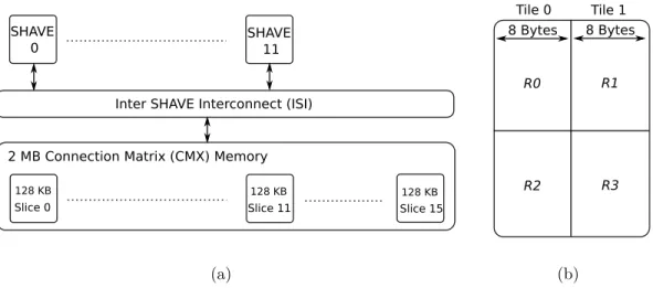
Myriad 2 contains 12 streaming hybrid architecture vector engine (SHAVE) and two reduced instruction set computing (RISC) processors. SHAVE processors are the real workhorse of Myriad 2 and are designed to crunch the complex imag-ing and vision algorithms [126]. The platform offers a 2 MB connection matrix (CMX) memory along with a number of programmable hardware accelerators for vision processing. Accelerators are connected to the CMX memory via a crossbar [107].
SHAVE is a VLIW processor containing a set of functional units which are fed with operands from three different register files [124]. The processor contains
Slice 0
Inter SHAVE Interconnect (ISI)
2 MB Connection Matrix (CMX) Memory
Slice 11 Slice 15 SHAVE 0 128 KB 128 KB 128 KB SHAVE 11 (a) R0 Tile 0 Tile 1 8 Bytes 8 Bytes R1 R2 R3 (b)
Figure 2.2: Organization of the CMX memory and its interface with SHAVE processors in Myriad 2. Memory is divided into slices (a) and each slice is divided into regions (b).
optimized functional units such as a branch and repeat unit (BRU), a compare and move unit (CMU), arithmetic units, and two load-store units (LSUs). Each SHAVE processor can execute two load-store instructions simultaneously.
2.5.1
CMX Memory
As shown in Figure 2.2(a), the 2 MB CMX memory is divided into 16 different slices, each with a size of 128 KB. A slice can hold both instructions and the data for a program running on a processor. Each of the first twelve slices (i.e., slice 0–slice 11) has an affinity to 1 of 12 SHAVE processors. Since Myriad 2 is a non-uniform memory access (NUMA) platform, it is more efficient in terms of latency and energy consumption for a processor to access its local slice (i.e., slice 0 for SHAVE 0). However, processors can also access any other slice in the CMX memory but with a higher latency. Therefore, placement of data in the local slice of a processor is recommended.
A slice is further divided into four regions, named R0, R1, R2, and R3 in Figure 2.2(b), each with a size of 32 KB. In principle, the architectural design
of the CMX memory allows four simultaneous memory accesses in four different regions of a given slice. Each region is a single physical block of random access memory (RAM) with a single chip select and a single set of address and data paths. Therefore, simultaneous memory accesses in the same region are not rec-ommended as they result in stall cycles due to clash among memory ports. Since a SHAVE processor has only two LSUs, only two simultaneous memory accesses are practically possible into a single CMX slice. Simultaneous memory accesses can be performed in any of the two different regions, e.g., R0 and R1 or R0 and R2.
Although Myriad 2 features a high bandwidth memory subsystem, its compiler schedules memory accesses inefficiently. The basic reason is that compiler is unaware of the memory organization. This results in unnecessary memory stalls and hence higher execution time for applications. In Chapter 4, we propose an optimization based on classification of memory references and taking advantage of memory organization to reduce memory bound stalls. In the following section, we present a brief survey of various approaches adopted in previous work for reduction of memory bound stalls.
2.6
Prior Work on Reduction of Memory Bound
Stalls
Memory bound stalls cause under-utilization of the compute logic due to mem-ory latency and hence become a major hurdle in improving the execution time of an application [128]. Various approaches have been proposed to reduce memory stalls, such as data mapping in multi-bank environment, using non-uniform mem-ory access (NUMA)-based design and architectural improvements in the memmem-ory and compute fabric.
simultaneously requested data on different memory banks. Researchers have pre-sented proposals to implement data mapping as a back-end compiler optimiza-tion [129, 130] as well as by analyzing memory access pattern at higher levels [131, 132, 133] for single-processor systems. Other works, such as [134, 135], pro-pose approaches for mapping data of different applications to multiple memory banks in a multi-core environment.
NUMA is commonly used in modern multi-processor systems to avoid the bottleneck of shared memory accesses [136]. It provides asymmetric memory bandwidth and latency characteristics [137]. In other words, cost of accessing data located in remote memory modules is higher than accessing data blocks in local memory modules. Memory affinity is a way to reduce this cost by placing the data in memory modules closer to the processor executing the computation thread [138] and guarantees to improve memory bandwidth and latency [139].
Many researchers have contributed in the context of memory affinity to reduce memory access cost on NUMA platforms. For example, a NUMA API for Linux was proposed in [140] which allows programmers to make memory allocations from a specific node or memory module, in addition to binding threads to specific CPUs. Different algorithms have been proposed to spread application data across different memories of a NUMA platform, such as round-robin, first touch affinity and next-touch affinity [136, 141]. An extension to Linux kernel to add support for the affinity-on-next-touch algorithm is reported in [142].
In this work, we exploit the availability of dual load-store units to processors of a vision-processing system and its NUMA architecture, where memory is divided into multiple slices, each one having an affinity to one of the processors. Unlike the traditional memory affinity approach focusing on the reduction of latency by placing data closer to the computing processor [136, 137, 141, 143], the purpose of our affinity analysis is to reduce the memory bound stalls by taking into account memory organization and hence efficiently scheduling memory accesses.
Another approach to reducing memory stalls, more related to our work, is op-timization of the memory subsystem of the execution platform and related archi-tectural components of the compute fabric. Like Myriad 2 platform, Snapdragon 800 [144], MaPU [121], and TI AcceleratorPac [122] use VLIW processors as main execution units [24] combined with RISC cores and other dedicated components. Unlike these systems using unified memory, Myriad 2 uses NUMA architecture enabling multiple cores to access their local memory slices simultaneously and hence make a contribution in reducing memory stalls.
Hexagon DSP on Snapdragon 800 is a VLIW featuring two data units. Each data unit is capable of executing a load, a store or an ALU instruction but unable to pack two memory accesses with one or more ALU instructions in a single cycle. On the other hand, VLIW processors of Myriad 2 are capable of packing two memory accesses with up to two ALU instructions in a single cycle. MaPU platform contains ten processing cores with unified memory scheme. A core can make up to three memory accesses simultaneously but into differ-ent physical memories. Furthermore, a physical memory cannot be accessed by different cores simultaneously. As compared to MaPU, Myriad 2 supports simul-taneous accesses to memory at two levels. First, multiple cores can access their local memory slices simultaneously due to NUMA architecture. Second, each core can make up to two simultaneous accesses into its local slice.
As noted by designers of MapU [121], compilers are a major source of the lower performance of execution platforms as they use a simplified model of processor architecture and do not consider detailed architectural features of the platform. Since our proposed compiler optimization is based on comparatively better archi-tectural features of Myriad 2 platform (such as dual load-store units per processor and a high bandwidth memory subsystem), as shown in Table 2.1, it is not only different than Hexagon DSP and MaPU, but has a potential of achieving higher performance.
Table 2.1: Comparison of architectural features of different CV platforms (read DNA as “Details not available”).
Platform Uses NUMA
architecture
Support for pack-ing more than two
memory
instruc-tions with an ALU instruction
Support for mul-tiple simultaneous accesses by a
sin-gle processor to
the same physical memory. Snapdragon 800 (with Hexagon DSP) No No Yes MaPU No Yes No TI Acceler-atorPAC No DNA DNA
Myriad 2 Yes Yes Yes
2.7
Network-on-Chip Routing
A System on Chip (SoC) consists of multiple Processing Elements (PEs) on a sin-gle chip. An NoC is a communication medium among PEs in a SoC [145]. Most current NoC architectures employ a 2D mesh topology [146] where processing elements are arranged in form of rows and columns connected through commu-nication links. Data injected by PEs into mesh, through network interfaces, is routed across mesh through routers. Figure 2.3 shows 16 PEs connected through a 4x4 mesh.
A router implements a routing algorithm to transport data from a source to a destination PE. Performance of a routing algorithm is affected by traffic pattern which is determined by behavior of active communication flows of an application. As an application’s tasks, mapped on different PEs, may not communicate always at the same data rate, its traffic pattern may change during execution.
A given routing algorithm may perform well for one traffic pattern but give poor results for others. Therefore, applying a single routing algorithm for whole
Router
Network adapter Link
PE1 PE2 PE3 PE4
PE5 PE6 PE7 PE8
PE9 PE10 PE11 PE12
PE13 PE14 PE15 PE16
Figure 2.3: 16 PEs connected through a 4x4 mesh NoC.
execution period of an application limits the network throughput. In Chapter 5, we present a selection scheme for selecting an appropriate NoC-routing algorithm with changes in the traffic pattern of an application. In the following subsection, we present a brief survey of prior work on reconfiguring NoC routing algorithms and highlight differences of our approach.
2.7.1
Prior Work on Reconfiguring Noc Routing
Algo-rithm
Many of Dynamically Reconfigurable NoCs (DRNoCs) can be reconfigured in terms of architecture or routing algorithm, for example, DyNoc [147], CoNoChi [148] and DRAFT [149]. In order to take care of the dynamically changing ar-chitecture in DyNoC, XY routing algorithm is adapted to deal with obstacles created by the dynamic placement and removal of modules. CoNoChi generates a routing table whenever topology changes and tables are then distributed via the network. In DRAFT, a hierarchal level dependent mask is used by each router
to determine if the received flit is to be moved upward [150].
All of the above mentioned DRNOCs reconfigure a particular routing algorithm to make it compatible with the modified network architecture. However, in our approach network architecture is fixed. We use a static mesh network and focus on switching the routing algorithm to take advantage of variations in traffic pattern during execution for improving throughput.
In [44], DyAD routing technique is described which selects between two rout-ing algorithms (a deterministic and an adaptive one) based on the congestion threshold and congestion flags. However, we investigate the possibility of mak-ing selections among a deterministic algorithm, such as XY routmak-ing, and multiple adaptive algorithms (for example, west-first, negative-first and north-last routing) based on the measurement of congestion level.
Chapter 3
Integrating NVM in Memory
Hierarchy of a DBMS
In this chapter, we first discuss the possible memory hierarchy designs when in-cluding NVM in a DBMS. We then describe currently available system software to manage NVM. We also explain the high-level modifications necessary in a traditional disk-optimized DBMS in order to take full advantage of NVM hard-ware. As a case study, we apply these modifications on storage engine (SE) of PostgreSQL.
Our modified SEs of PostgreSQL show performance improvement. However, the performance is limited by data readiness problem. Therefore, in this chapter, we also describe a general purpose library to prefetch data using known techniques like helper threads. In Chapter 6, we evaluate modified SEs with and without usage of library services.
Queries Intermediate data
in DRAM Database in disk
(a) Traditional design
Queries Intermediate data in NVM Database in NVM (b) All-in-NVM Queries Intermediate data in DRAM Database in NVM (c) NVM-Disk
Figure 3.1: NVM placement in the memory hierarchy of a DBMS.
3.1
Memory Hierarchy Designs for an
NVM-Based DBMS
With features of byte-addressability, low latency and high capacity, NVM has the potential to replace traditional disks as well as main memory [80]. Figure 3.1 shows different options that might be considered when including NVM into the system. Figure 3.1(a) depicts a traditional approach, where the intermediate state - including logs, data buffers, and partial query state - is stored in DRAM to hide disk latencies for data that is currently in use; while the bulk of the relational data is stored in a disk.
Given the favorable characteristics of NVM over the other technologies, an option might be to replace both DRAM and disk storage using NVM (Figure 3.1(b)). However, such a drastic change would require a complete redesign of current operating systems and application software. In addition, NVM technol-ogy is still not mature enough in terms of endurance to be used as a DRAM replacement. Hence, we advocate for a platform that still has a layer of DRAM memory, like [151], where the disk is completely or partially replaced using NVM, as shown in Figure 3.1(c) (NVM-Disk).
Using this approach, we can retain the programmability of current systems by still having a layer of DRAM, thereby exploiting DRAM’s fast read and write access latencies for temporary data structures and application code. In addition, it allows the possibility to directly access the bulk of the database relational data