NOVEL MATERIALS AND TECHNIQUES
FOR ENERGY CONVERSION AND
SENSING
a dissertation submitted to
the graduate school of engineering and science
of bilkent university
in partial fulfillment of the requirements for
the degree of
doctor of philosophy
in
materials science and nanotechnology
By
Okan ¨
Oner Ekiz
December 2015
Novel Materials and Techniques for Energy Conversion and Sensing By Okan ¨Oner Ekiz
December 2015
We certify that we have read this dissertation and that in our opinion it is fully adequate, in scope and in quality, as a dissertation for the degree of Doctor of Philosophy.
Aykutlu Dana(Advisor)
Ceyhun Bulutay
Ali Kemal Okyay
Adil Denizli
Hatice Duran
Approved for the Graduate School of Engineering and Science:
Levent Onural
ABSTRACT
NOVEL MATERIALS AND TECHNIQUES FOR
ENERGY CONVERSION AND SENSING
Okan ¨Oner Ekiz
Ph.D. in Materials Science and Nanotechnology Advisor: Aykutlu Dana
December 2015
In the recent years, characterization of nanomaterials and using them in sensing applications gain considerable attention. Increased research on nanotechnology brings new materials and techniques that come with many unsought properties. Additionally, novel materials and concepts have created new demands for new characterization techniques. In this thesis, our main aim is to characterize novel materials and develop new techniques to use nanotechnology in sensing applica-tions.
Graphene is one of the most important material in nanotechnology found in the recent years. In this thesis, we have characterized and explain the electrochem-ical behavior of graphene oxide. During the experiments, novel properties of graphene oxide have been revealed. Foundings paved the way for new applica-tions of graphene.
Recent studies in plasmonic materials made SERS (Surface-Enhanced-Raman-Spectroscopy) an important characterization tool used in nanotechnology. SERS is a powerful technique for chemical specific and label free analysis of low con-centration materials. In this thesis, we have used SERS to build an artificial nose for detection of VOCs. SERS substrates have been fabricated and used for the experiments. Experiments showed that our technique could detect many VOCs and could be used for several applications such as explosive and drug detection. There is a strong need for easy and cost effective biosensors especially for home-care applications. Recent advances in nanotechnology help us to develop cost effective techniques. Reducing costs could make biosensors more accessible for end user applications such. In this thesis, we have developed a biosensor platform by using SPR (Surface Plasmon Resonance) for pathogen detection. Experiments showed that our device could detect 102 pathogens without labeling. Our aim is
to improve this platform for rapid food analysis and home-care applications. Keywords: Graphene, Graphene oxide, Raman microscopy, SERS, Surface
plas-¨
OZET
ENERJ˙I C
¸ EVR˙IM˙I VE ALGILAMA AMAC
¸ LI
YEN˙IL˙IKC
¸ ˙I MALZEMELER VE TEKN˙IKLER
Okan ¨Oner Ekiz
Malzeme Bilimi ve Nanoteknoloji, Doktora Tez Danı¸smanı: Aykutlu Dana
Aralık 2015
Nanomalzemelerin karakterizasyonu ve sens¨or teknolojilerde kullanımı son yıllarda ciddi miktarda ¨onem kazanmı¸stır. Nanomalzemeler ¨uzerine yapılan ara¸stırmaların artması farklı malzemelerin ve tekniklerin bulunmasını sa˘glamı¸stır. Yeni malzemeler, ara¸stırılmayı bekleyen bir ¸cok ¨ozellik ihtiva etmekte-dir. Ek olarak, farklı karakterizasyon tekniklerinin geli¸stirilmesi i¸cin talep olu¸sturmaktadır. Bu tez ¸cal¸smalarında amacımız yeni malzemeleri karakterize edip, nanoteknolojiyi kullanarak uygulamalar geli¸stirmektir.
Grafen son yıllarda bulunmu¸s nanoteknoloji alanındaki en ¨onemli malzemeler-dendir. Bu tez ¸calı¸smaları sırasında, Grafen karakterize edilip, elektrokimyasal davranı¸sları aıklanmı¸stır. Yapılan deneylerde, grafen oksitin bazı yeni ¨ozellikleri ortaya ıkarılmı¸stır. Elde edilen bulgular Grafenin yeni uygulamalarının yolunu a¸cmı¸stır.
Son yıllarda plazmonik alanında yapılan ¸calı¸smalar SERS (Y¨uzey Y¨ukseltilmi¸s Raman Spektroskopisi)0i nanoteknoloji alanında kullanılan ¨onemli bir karakteri-zasyon aracı haline getirmi¸stir. SERS, d¨u¸s¨uk konsantrasyonlu malzemeler i¸cin kimyasal belirli i¸saretlemesiz bir analiz yapabilen g¨ul¨u bir tekniktir. Bu tez ¸calı¸smalarında, SERS0 i kullanarak u¸cucu organik kimyasalları tesbit edebilen yapay burun yapılmı¸stır. Deneylerde kullanılan SERS substratları ¨uretilmi¸stir. Yapılan deneyler g¨ostermektedirki, kullandıımız teknik bir ¸cok u¸cucu organik kimyasalı tesbit edebilmektedir ve patlayıcı ve uyu¸sturucu tesbiti gibi bir ok alanda kullanılabilmektedir.
Ki¸sisel ve ev uygulamaları i¸cin d¨u¸s¨uk maliyetli ve kolay kullanımlı biyosens¨or sistemleri i¸cin ihtiya¸c vardır. Nanoteknoloji alanındaki geli¸smeler, uygun maliyetli tekniklerin geli¸stirilmesinde bize yardımcı olmaktadır. Maliyetlerin d¨u¸s¨ur¨ulmesi, biyosens¨orlerin son kullanıcılar i¸cin daha ula¸sılabilir yapabilmek-tedir. Bu tez alı¸smalarında, y¨uzey plazmon rezonans tekniini kullanılarak gıda sulularının tesbitini yapan bir biyosens¨or platformu ¨uretilmi¸stir. Yapılan deneyler
v
g¨ostermektedir ki, geli¸stirilen cihaz yakla¸sk 100 su¸cluyu i¸saretlemesiz olarak tes-bit edebilmektedir. Amacımız geli¸stirilen bu platformu , hızlı gıda analizi ve son kullanıcı uygulamaları i¸cin geli¸stirmektir.
Acknowledgement
First, I would like to thank my advisor Dr.Aykutlu Dana for his continuous guidance throughout my PhD. He always encouraged and supported me with novel ideas. Seven years with Dr.Dana was a great experience and will always be remembered.
I owe my sincere thanks to Prof. Dr. H. ˙Ibrahim Ekiz. He generously allowed me to use his cell culture facilities in Mersin University. I would like to thank Esma Eser, Hikmet C¸ elik and Selim S¨ulek for their support and friendship during the experiments.
I would like to thank all the people contributed to this thesis, Dr. Ali Kemal Okyay, Dr. Ceyhun Bulutay, Dr. Adem Yildirim, G¨oksu C¸ ınar, Prof.Dr. Engin Umut Akkaya, Dr. Mustafa G¨uler, Bihter Da˘glar, Dr. Turgay Tenikay, Dr. Burak T¨urker, Sıla Toks¨oz, Dr. Handan Acar, Merve T¨urk¸sanli Kaplan, Hasan Guner, Mustafa ¨Urel, Dr. Sencer Aya¸s, Koray Mizrak, and all the past and present members of UNAM. I would like to thank my best friend Sinan Baysal.
Last but most important, I would like thank my family who always believed in and supported me. I wish to give special thanks to Melis S¸ardan Ekiz, who stood by me for all those times.
Contents
1 Introduction 1
2 Reversible Electrical Reduction and Oxidation of Graphene
Ox-ide 4
2.1 Introduction . . . 4
2.2 Synthesis of graphene oxide . . . 5
2.3 Experimental . . . 6
2.4 Reversible oxidation and characterization of graphene . . . 7
3 Tunable Ultrafast Optical Response of Graphene Oxide 21 3.1 Introduction . . . 21
3.2 Experimental . . . 22
3.3 Characterization and ultrafast optical response . . . 23
4 Surface-Enhanced Raman Spectroscopy of Volatile Organic Compounds 29 4.1 Introduction . . . 29
4.2 Chemical synthesis, fabrication and characterization of SERS sub-strates . . . 30
4.3 Single molecule sensing with SERS . . . 31
4.4 Portable Raman microscope . . . 45
5 Food Pathogen Detection with Surface Plasmon Resonance 49 5.1 Introcution . . . 49
5.2 Theory . . . 50
CONTENTS viii
5.3.1 Microorganisms . . . 52
5.3.2 Reagents . . . 52
5.3.3 Preperation of Gold Surfaces . . . 53
5.3.4 Immobilization of antibodies . . . 53
5.3.5 Detection of bacteria . . . 53
5.4 Device construction . . . 55
5.5 Optimization of experimental conditions . . . 58
5.6 Surface functionalization . . . 65
5.7 Pathogen Detection . . . 69
List of Figures
2.1 Thin multilayer graphene oxide films (30-60 nm thickness) can be electrically reduced and oxidized. The two terminal device is schematically shown. Two therminal device was fabricated by sputtering Au-Pd on a glass substrate with a shadow mask. . . 8 2.2 Oxidation and reduction are confirmed by XPS measurements.
The oxygen-to carbon ratio is measured using a 100 µm diame-ter photoelectron collection spot and is plotted as a function of distance across the device. The data show gradual changes in the stoichiometry between the contacts. . . 9 2.3 (a) Linear optical transmission of the films is measured using a 25
µm core fiber optic light collector near one of the contacts while the bias is swept between -2.5 and 2.5 V. It is observed that wavelength dependent transmission is adjustable by applying an external bias. Representative XPS spectra that correspond to the (b) reduced and (c) oxidized states show the correlation of optical transparency with stoichiometry. . . 11
LIST OF FIGURES x
2.4 Figure 2.4: (a) Tunneling current images showing the effect of reversible electrical oxidation and reduction in three consecutive voltage cycles (+2 V, -2 V, +2 V for tens of seconds). The im-ages are collected at the same location, by grounding the two con-tacts and applying a 10 mV tip bias. The surface conductivity is observed to switch in reduced and oxidized states. (b) Represen-tative optical micrographs (observed by bright-field transmitted light, scale bar 30 µm) of multilayer graphene oxide films show spatially uniform transmission at the beginning of the bias cycles (left), where reduced transmission is observed upon application of bias that reduces the left side of the film (middle, minus sign, dark region). The optical transmission can be manipulated by reversing the polarity of applied bias and causing the left side to oxidize and the right side to reduce (right). . . 12 2.5 (a) Optical micrographs recorded as a function of time show the
progress of reduction and oxidation upon sudden reversal of bias polarity. The arrows denote the presence of an advancing reduction front. (b) Failure of the device is observed upon application of a large bias (3 to 10 V for a given device geometry). Failure is due to advancement of dentrite-like conductive (reduced) regions, eventually causing a short in the device. . . 13 2.6 (a) Partially reduced graphene oxide films are investigated by
mul-tifrequency electrostatic force microscopy. Regions with different surface potentials are observed, suggesting the presence of a 2D graphene heterostructure where graphene and graphene oxide do-mains are simultaneously present. Electrostatic force amplitude is imaged, where bright regions correspond to lower surface poten-tial, or greater oxygen content. (b) Higher resolution electrostatic force map shows that segregated regions with distinct surface po-tentials are present, with sizes ranging from few nanometers to tens of nanometers. . . 14 2.7 Due to the local electric field induced by a conductive atomic force
LIST OF FIGURES xi
2.8 Cyclic current versus voltage (I-V) measurements are performed on multilayer graphene oxide films on Au/Pd film using a Pt-coated atomic force microscope cantilever. An increase of the current at smaller bias voltage after successive (1 to 7) I-V measurements suggests a decrease in the local effective band gap. Despite a sym-metric voltage sweep, a net reduction effect is observed, suggesting that oxidation rate is smaller than reduction rate at similar mag-nitude bias. . . 16 2.9 Tunneling current map after the first I-V measurement shows no
or little surface conductivity. (d) Tunneling current map obtained after the 7thI-V measurement shows increased current on one flake (or few flakes), suggesting whole individual flakes are reduced. Dashed red contour shows the reduced region and arrow denotes the location of the cantilever tip. . . 17 2.10 (a) Multilayer graphene oxide films, which have not been subject
to thermal or electrical reduction shows low surface conductivity as observed by tunneling current maps obtained with a Pt tip (10 mV bias). (b) Upon partial reduction, conductive domains are observed in the tunneling current maps. (c) Tunneling current maps of chemically or thermally reduced multilayer graphene films show plateaus of current instead of conductive spots. (d) Cyclic current-voltage measurements are performed on two-terminal de-vices with unreduced graphene oxide. Hysteresis and changes in the I-V curves show that graphene oxide films feature both resis-tive switching and capaciresis-tive charge storage. (e) Hysteresis is de-creased for two-terminal devices fabricated using partially reduced graphene oxide films, and (f) no observable hysteresis is present in multilayer graphene films obtained by complete thermal reduction (150 ◦C, few minutes thermal exposure) of graphene oxide films. . 18
LIST OF FIGURES xii
3.1 Color online schematic description of the device used in the mea-surements. (b) The applied bias voltage profile and (c) normalized differential probe transmission A as defined in text are plotted as a function of wavelength and time. Wavelength dependent switch-ing between saturable and NA is observed upon application of the bias pump excitation energy of 0.5 J, center wavelength of 790 nm, pulse width of 44 fs. The dashed lines are guidelines for the eyes, delineating the transition wavelength between saturable and NA. (d) Differential absorption A plotted as a function of wave-length for three representative points with different bias conditions regions I, II, and III in cshowing NA and SA. . . 24 3.2 A color online differential absorption of probe at zero pump-probe
delay. ac show voltage bias dependence. df Changes in the re-sponse upon high-intensity pump exposure for various durations. Similar changes are observed for electrochemical and photothermal reduction. . . 25 3.3 Color online (a) temporal behavior of the saturated and NA
re-sponses at different probe wavelengths after applying bias voltage. (b) Temporal behavior of the saturated and NA responses at 750 nm probe wavelength depending on the exposure time to pump pump excitation energy of 5 J, center wavelength of 790 nm, pulse width of 44 fs. . . 27
4.1 Image of 3nm silver coated glass slide. . . 31 4.2 Absorbance vs wavelength of 3nm silver coated glass slide. . . 32 4.3 Absorbance vs wavelength of 3nm silver coated glass slide just after
fabrication and 1 week after fabrication. . . 33 4.4 Absorbance vs wavelength of 3nm silver coated glass slide and after
heat treatment. . . 34 4.5 Total intensity of Raman signal vs time of a blank SERS substrate. 36 4.6 Total intensity of Raman signal vs time of a SERS substrate
cov-ered by 4-MBA monolayer. . . 37 4.7 SERS spectra of 4-MBA. When 4-MBA goes into physical
LIST OF FIGURES xiii
4.8 (b) Time vs total intensity Raman signal of blank substrate. (a) Time vs differential of Raman signal. (c) Raman spectrum at the
peak shown by black arrow. . . 39
4.9 Microscope image of fragrance thin film on SERS substrate. (a) is unexposed film, (b) Laser light induces a repelling force, (c) Laser is closed and thin film covered the surface again. . . 40
4.10 Average surface-enhanced Raman spectrum of TNT. . . 41
4.11 Average surface enhanced Raman spectrum of 4-MBA. . . 42
4.12 Average surface-enhanced Raman spectrum of Lauric acid. . . 43
4.13 Time series of a filtered Raman spectra of a SERS substrate. A TNT sample was placed near SERS substrate. Total Raman sig-nal wavelength filtered with TNT peak positions obtained from average surface-enhanced Raman spectrum of TNT. The peak at approximately 35th sec. is assumed to be a TNT molecule diffused into the hot spot. . . 43
4.14 Captured Raman signal from blank SERS substrate vs SERS fin-gerprint of TNT. A TNT sample was placed near SERS substrate. 44 4.15 Optical design of the portable Raman system. . . 46
4.16 Technical drawing of portable Raman System. . . 47
4.17 Photo of Portable Hyperspectral Raman System. . . 48
5.1 Shematic presentation of food pathogen detection with surface plasmon resonance. . . 50
5.2 Photo of incubated pathogens. . . 54
5.3 Calculated reflected intensity vs of 47nm Au film at (a) 633nm and (b) 850nm wavelength. . . 56
5.4 Wavelength vs. transmission graph of the polarizer. . . 57
5.5 (a) Original and (b) filtered pixel vs reflected light intensity in SPR. 59 5.6 Change in the resonance angle vs time. Saw-like decrease is shown before correction in the software. . . 60
5.7 Resonance angle vs time after device opening. . . 60
5.8 Resonance angle change during a PBS pulse send in water filled flow channel with 500 um height. . . 61
LIST OF FIGURES xiv
5.10 Resonance angle change during a PBS pulse send in water filled flow channel with 100 um height. . . 62 5.11 Modified PTFE channel is shown. In this channel design, the
in-teraction of fluid with o-ring is prohibited. . . 63 5.12 Photo of the sample holder of the device after an experiment. The
fluid channel is filled with water during the removal of the PTFE channel. . . 63 5.13 Average resonance angle with respect to flow speed. . . 64 5.14 Photo of EDC-NHS reaction in an Eppendorf. Bubbles formed
during the preparation of the mixture. . . 66 5.15 Time vs resonance angle during the 400:100 mM EDC-NHS pulse
pumped into the SPR device. . . 67 5.16 Time vs resonance angle during the 200:100 mM EDC-NHS pulse
pumped into the SPR device. . . 68 5.17 Surface functionalization of the SPR chip surface with salmonella
antibody. . . 69 5.18 Changes in resonance angle during the functionalization of the Au
surface and S. Enteritidis flow. . . 71 5.19 Average resonance angle with respect to S. Enteritidis concentration. 72 5.20 Changes in resonance angle during functionalization steps and L.
monocytogenes flow. . . 73 5.21 SEM images of Sal-ab functionalized SPR chip after S. Enteritidis
flow. . . 74 5.22 SEM images of Sal-ab functionalized SPR chip after L.
monocyto-genes flow. . . 75 5.23 Resonance angle change vs pathogen contaminated whole milk
with different concentrations. Blue line is the original signal. For better demonstration red line is calculated average resonance angle of each concentration. . . 76 5.24 Change in the resonance angle during L.monocytogenes flow on
LIST OF FIGURES xv
5.25 Average resonance angle vs serial dilution of L.monocytogenes. The SPR chip is functionalized with antibody. Listeria-5 is equals to 2Listeria-50 pathogens, Listeria-4 is equal to 2Listeria-500 pathogens, Listeria-3 is equal to 25000 pathogens, Listeria-2 is equals to 250000, Listeria-1 is equals to 2500000 and Listeria is equals to 25000000 pathogens. . . 80 5.26 Average resonance angles vs serial dilution of E.coli. The SPR
chip is functionalized with listeria antibody. Ecoli-7 is equals to 10 pathogens, Ecoli-6 is equal to 100 pathogens, E-coli5 is equal to 1000 pathogens, E-coli1 is equals to 10000000 pathogens. . . . 81 5.27 Resonance angle vs serial dilution of E.coli on anti-listeria antibody
functionalized SPR chip. . . 82 5.28 Resonance angle change during the Salmonella detection. After
flow of Salmonella with 103 concentration, the pump is stopped to
observe growth. . . 83 5.29 Resonance angle change during the Salmonella growth. The data
List of Tables
5.1 Starting bacterial dilutions . . . 54 5.2 Calculated statistical values of resonance angle with different flow
speeds . . . 64 5.3 Average change in the resonance angle with the amount of
strep-tavidin. . . 65 5.4 Average change in the resonance angle with the amount of
salmonella antibody. . . 66 5.5 Calculated statistical values of resonance angle during L.monocytogenes
detection experiment . . . 78 5.6 Calculated statistical values of resonance angle during the
cross-contamination experiment; E.coli flow on listeria antibody func-tionalized SPR chip. . . 79
Chapter 1
Introduction
In the recent years, the design and fabrication of nanomaterials for chemical and biological sensing have received considerable attention due to the increased de-mand for low-cost practical applications. Although, great amount of research progress has been done in nanomaterials, there are still uncharacterized proper-ties of new materials such as electrochemical behaviour of graphene. Complete characterization of common nanomaterials is critical for practical applications. Graphene is one of the most important materials in nanotechnology. In this the-sis, we have revealed novel properties of graphene and found new applications. Additionally, we have developed sensors by using SERS (Surface Enhanced Ra-man Spectroscopy) and SPR (Surface Plasmon Resonance) techniques.
In Chapter 2, we demonstrate that graphene oxide can be reversibly reduced and oxidized using electrical stimulus. Controlled reduction and oxidation in two-terminal devices containing multilayer graphene oxide films are shown to result in switching between partially reduced graphene oxide and graphene, a process which modifies the electronic and optical properties. High resolution tunnel-ing current and electrostatic force imagtunnel-ing reveal that graphene oxide islands are formed on multilayer graphene, turning graphene into a self-assembled het-erostructure random nanomesh. Charge storage and resistive switching behavior is observed in two-terminal devices made of multilayer graphene oxide films,
cor-demonstrated. Results are discussed in terms of thermodynamics of oxidation and reduction reactions
In Chapter 3, we demonstrate reversible and irreversible changes in the ultrafast optical response of multilayer graphene oxide thin films upon electrical and op-tical stimulus. The reversible effects are due to electrochemical modification of graphene oxide, which allows tuning of the optical response by externally applied bias. Increasing the degree of reduction in graphene oxide causes excited state absorption to gradually switch to saturable absorption for shorter probe wave-lengths. Spectral and temporal properties as well as the sign of the ultrafast response can be tuned either by changing the applied bias or exposing to high intensity femtosecond pulses.
In Chapter 4, we demonstrate single molecule sensing of airborne molecules with Raman spectroscopy. Sensing mechanism is based on Raman scattering of hop-ing volatile organic compounds (VOCs) on surface-enhanced Raman spectroscopy (SERS) substrates. The demonstrated sensor can discriminate even residual fra-grance molecules of cleaning products used around experimental set-up. Addi-tionally, we showed that excess amount of target molecules could not saturate the sensor contrary to mammalian olfactory system. Experiments revealed that sen-sor surface repels excess molecules with a light driven force. This phenomenon could be observed on sensor surface dip-coated with target molecules. Videos of light driven motion will be shown in the presentation. Spectra coming from SERS substrates are complicated and contain extensive amount of information to process manually. We have developed several algorithms to process and identify Raman spectra of hoping molecules.
In Chapter 5, we report rapid and sensitive detection of Salmonella Enteritidis and Listeria with high specificity by using SPR (Surface Plasmon resonance) technique. Antibodies against S. Enteritidis and Listeria were immobilized on to a gold sensor surface and different concentrations of serially diluted bacterial solutions were pumped in to the system. The changes in the response unit (RU) due to the binding of different concentrations of bacteria were measured. Regen-eration of the sensor surface was carried out by using PBS + Tween 80 solution. The selectivity of the developed sensor was examined with different bacterial
species which did not produce any significant response. Additionally, the abil-ity of the developed sensor to detect S. Enteritidis in milk samples was tested. Based on these results, the developed SPR based biosensor may be used for rapid, label-free, sensitive and selective detection of bacteria in food materials.
Chapter 2
Reversible Electrical Reduction
and Oxidation of Graphene Oxide
2.1
Introduction
Graphene [1, 2, 3] has received tremendous attention in recent years due to its potential applications in electronics[4, 5, 6], sensors[7, 8, 9], energy storage[10, 11, 12], and optics[13, 14, 15]. Despite the extreme intrinsic mo-bility of graphene,[16] semimetallic electronic band structure limited its use in high-performance transistors. Quantum confinement effects were theoretically [17, 18] and experimentally [19, 20] shown to modify the band structure, mak-ing graphene a more versatile material. Chemical modification is still being actively sought to form semiconductors in the graphene family and implement conventional optoelectronic device structures. Novel devices have been reported that combine the superior electronic properties of graphene with other chemical and mechanical phenomena, such as resistive switching and electromechanical memories.[21, 22, 23] The mechanism of observed resistive switching in some graphene-based devices remained unclear. Graphene oxide (GO) is an insula-tor with a large effective band gap and band structure that depends on the stoichiometry.[24, 25] It has been previously observed that graphene oxide can
be reduced controllably at low temperature (low-T) in ambient atmosphere.[26] In such a low-temperature reduction process, the resistivity of the films can be continuously monitored and can be used to control the degree of reduction. Inter-ruption of thermal reduction results in partially reduced graphene oxide (PRGO). Conduction mechanisms of such PRGO films are known to be different than multilayer graphene (MLG) films, as evidenced by temperature dependence of resistivity.[26, 27, 28] A hopping transport mechanism was thought to be domi-nant in such films, and limited evidence for the presence of oxygen-rich domains was provided through scanning tunneling microscopy (STM) imaging of PRGO layers.[29] Recently, thermal site selective reduction of graphene oxide is demon-strated using a heated atomic force microscope tip.[30] STM has also been used to image hydrogen atoms on graphene and to create nanoscale heterostructure patterns by tip induced hydrogen desorption.[31] Recently, a conductive atomic force microscopy tip was used to characterize nanoscale surface conductivity of graphene oxide, and tip-induced reduction was shown to be possible.[32] In this work, we demonstrate electrically induced reversible reduction of graphene oxide, resulting in changes in the electronic and optical properties of graphene-based thin films. It is observed that optical and electronic property changes are corre-lated with the formation of a graphene/graphene oxide nanomesh.
2.2
Synthesis of graphene oxide
Graphene oxide was synthesized from natural graphite (SP-1, Bay Carbon) by the Hummers method.[33] 25 ml of 66◦ sulfuric acid was cooled to 0 ◦C with an ice bath in a 100 ml glass beeker. 1g of powdered graphite and 0.5 g of NaNO3
were added to the sulfuric acid. While maintaining vigorous magnetic stirring, 3 g. of KMnO4 was added to the solution. The temperature was kept below 20 ◦C during the addition of KMnO
4. The ice-bath was removed and temperature
icreased to 35◦C for 30 minutes. Then, 50 ml of DI water was added slowly caused violent effervescence and increase in temperature to approximately 100 ◦C. The
diluted with 150 ml of DI water. Hydrogen peroxide was added to reduce the residual permanganate and manganese dioxide to colorless soluble manganese sulfate. After centrifugation of the solution at 8000 rpm for 30 minutes, the graphite oxide was precipitated and washed with DI water for three times with the same procedure. The graphite oxide DI water mixture was than ultrasonicated for 30 minutes. Ultrasonication exfoliated graphite oxide and dissolved it in DI water. To eliminate graphite and unexfoliated graphite oxide, the solution was centrifugated for 15 minutes at 14000 rmp. The bright yellow supernatant solution is the final product that is graphene oxide dissolved in DI water.
2.3
Experimental
Stable graphene suspensions were prepared by a fast and simple method. Hy-drazine hydrate (0.1 mL, Merck) was added to the 10 mL of graphene oxide/water, and the mixture was heated to 85◦C for 1 h. A few minutes after the addition of hydrazine hydrate, the color of the mixture became black. At the end of 1 h, the graphene particles precipitated because of aggregation. Acetone (Sigma-Aldrich) was added to the solution with the same volume. After hydrazine treatment, the graphene surface contained hydrazone groups[34]. Acetone could modify the sur-face graphene by reacting with hydrazone groups; therefore, addition of acetone dissolves graphene in the water and hydrazine hydrate mixture. To completely suspend aggregated graphene, 5 min of sonication was applied to the mixture. Two-terminal devices were fabricated by sputtering Au-Pd films on precleaned glass substrates by using a 300 µm wide shadow mask. Graphene or GO sus-pensions were drop-casted on the devices fabricated. The films were dried under vacuum. Devices were characterized using a digital source meter (Keithley 2700) with a probe station. Graphene devices were annealed at 125-150 ◦C for 30 sec before measurements. Partially reduced graphene oxide samples were prepared by thermal annealing of graphene oxide films at 125 ◦C for 30 sec. Thermal annealing processes were applied on a preheated hot plate. Electrochemical ex-periments were performed under ambient conditions in clean room conditions, at room temperature (T = 25 ( 0.5 ◦C) and 40 ( 5 % humidity as monitored
by a humidity sensor, under 1 atm pressure. Electrical and XPS (X-ray photo-electron spectroscopy) measurements were done on a Thermo K-Alpha system. Multifrequency electrostatic force microscopy was implemented using modified commercial silicon cantilevers with spring constants of 2-4 N/m, and resonance frequencies of 65-75 kHz. The tips are double-stage electron-beam induced de-posited Pt tips with a tip radius of 2-5 nm as inspected by scanning electron microscopy. Low-frequency electrostatic excitation was applied at 5 kHz, and first and second time harmonics of the electrostatic forces were monitored using lock-in amplifiers (Stanford Research Systems, SR 830). The details of the high resolution multi frequency electrostatic force microscopy and spectroscopy can be found in references [35, 36, 37].
2.4
Reversible oxidation and characterization of
graphene
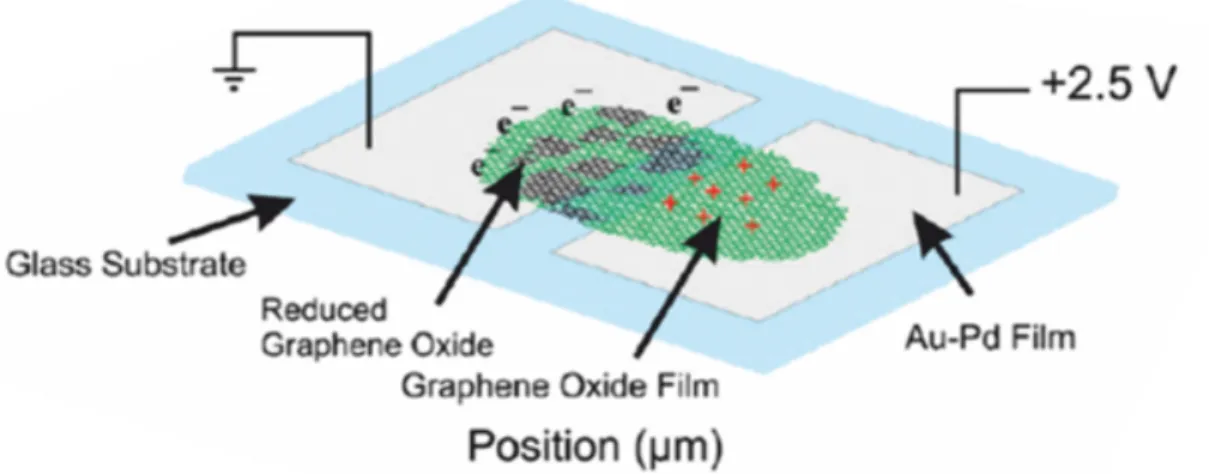
Electrical reduction of GO in air has been studied, using multilayer GO (MLGO) films deposited on metalized glass substrates. The two-terminal devices consist of thin (10-50 nm) Pd/Au planar contacts, separated by 0.3-0.6 mm, with a thin multilayer GO film covering both contacts and in between (Figure 2.1). Upon application of a bias to the contacts, the positive contact is seen to be oxidized and the negative contact is seen to be reduced. There is a potential drop between the contacts due to the finite conductivity of the films. Experiments showed that stoichiometry depends on the distance from the contacts, as confirmed by X-ray photoelectron spectroscopy (XPS) (Figure 2.2). The reduction/oxidation can be reversed by reversal of the bias.
Figure 2.1: Thin multilayer graphene oxide films (30-60 nm thickness) can be electrically reduced and oxidized. The two terminal device is schematically shown. Two therminal device was fabricated by sputtering Au-Pd on a glass substrate with a shadow mask.
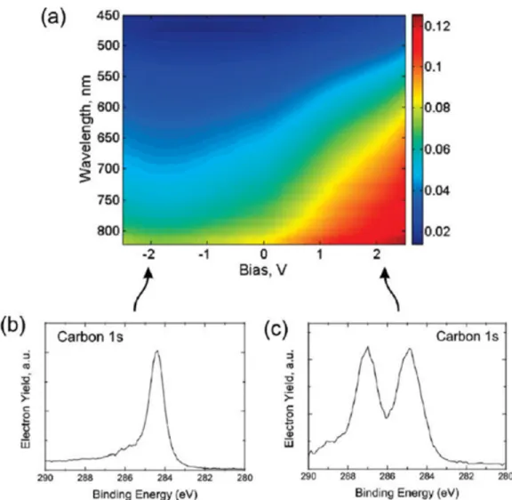
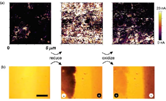
state. Wavelength-dependent linear transmission is measured using a fiber-coupled spectrometer near one of the contacts, while the bias is swept quasi-statically between -2.5 and 2.5 V. A gradual increase of the absorption edge as a function of applied bias is observed (Figure 2.3a). The optical transparency is correlated with the oxidation state (Figure 2.3b and c), films being semitrans-parent in the oxidized state. During cyclic voltage sweeps, it is observed that electrically induced oxidation/reduction takes place with time scales on the order of seconds for applied bias voltages of 2.5 V. We infer the thickness of the films to be 30-60 nm using optical measurements, assuming the films have absorption coefficients similar to graphene during the absorbing (reduced) state. [38] We in-spect the surface electronic properties of the two-terminal devices with an atomic force microscope (AFM), imaging the surface topography and conductivity before and after voltage pulses applied between its terminals. Two-terminal devices are subjected to voltage pulses (typically 2 to 3 V) while the tip is retracted. After the electrical reduction (or oxidation) process, the device contacts are grounded and the surface conductivity is imaged using a conductive AFM tip, using few mil-livolt tip bias. It is observed that the surface resistance of MLGO films decreases in the oxidized state, correlated with an increase in the optical transparency of the film (Figure 2.4a).
Figure 2.2: Oxidation and reduction are confirmed by XPS measurements. The oxygen-to carbon ratio is measured using a 100 µm diameter photoelectron col-lection spot and is plotted as a function of distance across the device. The data show gradual changes in the stoichiometry between the contacts.
changes in the optical transparency of the films are observed with the aid of the optical microscope in transmitted light mode in a separate experiment (Figure 2.4b).
It is observed that the transparent state corresponds to a mostly insulating surface with intermittent conductive domains. Upon application of a reducing pulse, the surface conductivity of the film greatly increases. It is seen that both the number of conductive domains and current per domain increase. When small currents (10 µA per mm wide films) are used, the reactions are slow and no signif-icant topographical change is observed as verified by contact mode AFM images. This suggests that electrical changes are related to the chemistry of the films and not due to a mechanical reconfiguration. Rapid reduction and oxidation, however, result in delamination of the flakes as evident by increased instability in noncontact AFM images (data not shown). A sequence of optical micrographs shows that oxidation or reduction is not instant and not simultaneously taking place over the film area, but progresses as a front (Figure 2.5a). This is possibly due to the coupling of the potential distribution inside the film depending on the conductivity, which in turn is related to the degree of reduction. It is also observed that, when low (¡2 V) maximum bias values are used, reversible opti-cal and resistive switching continue for multiple cycles (about 20 in our devices) before the film shows an irreversible reduction in electrical resistance. Our ob-servations suggest that previously observed resistive switching in graphene oxide and graphene devices is a result of chemical modification of graphene due to re-versible binding of oxygen[23, 24]. The drop-cast films consist of a large number of flakes. The thickness and conductivity of the films are not very uniform, and we attribute the device failure to formation of highly conductive dendrite-like shorting paths, which are observable in optical images (Figure 2.5b).
As the shorting paths are formed, current paths and voltage distributions inside the film change in a way that the bias needed for the reduction/oxidation process cannot be sustained uniformly and controllably at all parts of the film. We also investigate film surfaces in various oxidation states using high-resolution multi-frequency electrostatic force microscopy. Since electrostatic force microscopy is
Figure 2.3: (a) Linear optical transmission of the films is measured using a 25 µm core fiber optic light collector near one of the contacts while the bias is swept between -2.5 and 2.5 V. It is observed that wavelength dependent transmission is adjustable by applying an external bias. Representative XPS spectra that correspond to the (b) reduced and (c) oxidized states show the correlation of optical transparency with stoichiometry.
Figure 2.4: Figure 2.4: (a) Tunneling current images showing the effect of re-versible electrical oxidation and reduction in three consecutive voltage cycles (+2 V, -2 V, +2 V for tens of seconds). The images are collected at the same location, by grounding the two contacts and applying a 10 mV tip bias. The surface con-ductivity is observed to switch in reduced and oxidized states. (b) Representative optical micrographs (observed by bright-field transmitted light, scale bar 30 µm) of multilayer graphene oxide films show spatially uniform transmission at the beginning of the bias cycles (left), where reduced transmission is observed upon application of bias that reduces the left side of the film (middle, minus sign, dark region). The optical transmission can be manipulated by reversing the polarity of applied bias and causing the left side to oxidize and the right side to reduce (right).
Figure 2.5: (a) Optical micrographs recorded as a function of time show the progress of reduction and oxidation upon sudden reversal of bias polarity. The arrows denote the presence of an advancing reduction front. (b) Failure of the device is observed upon application of a large bias (3 to 10 V for a given device geometry). Failure is due to advancement of dentrite-like conductive (reduced) regions, eventually causing a short in the device.
a noncontact and relatively nondestructive measurement technique, we use it as a reliable complementary way of confirming the surface electronic structure. In the electrostatic force microscopy images, we see that there are interconnected domains of different work functions on the PRGO films (Figure 2.6a, b).
Brighter pixels correspond to regions with more negative surface potentials, which we attribute to the presence of bound oxygen and hydroxide. Darker regions correspond to graphene-like channels and quantum dots. Sizes of the graphene dots show a distribution and vary from nanometer to micrometer scale in various states. These observations confirm that partial electrical reduction re-sults in a graphene/graphene oxide heterostructure nanomesh, whose mesh size depends on the degree of reduction.
Figure 2.6: (a) Partially reduced graphene oxide films are investigated by multifre-quency electrostatic force microscopy. Regions with different surface potentials are observed, suggesting the presence of a 2D graphene heterostructure where graphene and graphene oxide domains are simultaneously present. Electrostatic force amplitude is imaged, where bright regions correspond to lower surface po-tential, or greater oxygen content. (b) Higher resolution electrostatic force map shows that segregated regions with distinct surface potentials are present, with sizes ranging from few nanometers to tens of nanometers.
This observation is in accord with previous theoretical predictions. Uniform coverage of graphene oxide is not energetically favorable.[24, 25] Tip-induced elec-trical oxidation of graphene oxide is demonstrated by using a conductive AFM tip operated in the contact mode. Application of a positive sample bias (1-2 V) results in oxidation of graphene films, and resulting GO structures can be observed in the tunneling current image collected with a few millivolt tip bias (Figure 2.7).
No oxidation is observed for biases under 0.5 V. Reduction of MLGO is ob-served to occur when the sample is negatively biased. In order to monitor the changes in the electronic properties of the MLGO film surface as a function of bias, the tunneling current is measured between the Pt-coated AFM tip and the MLGO film while the sample potential is swept in a cyclic fashion (Figure 2.8).
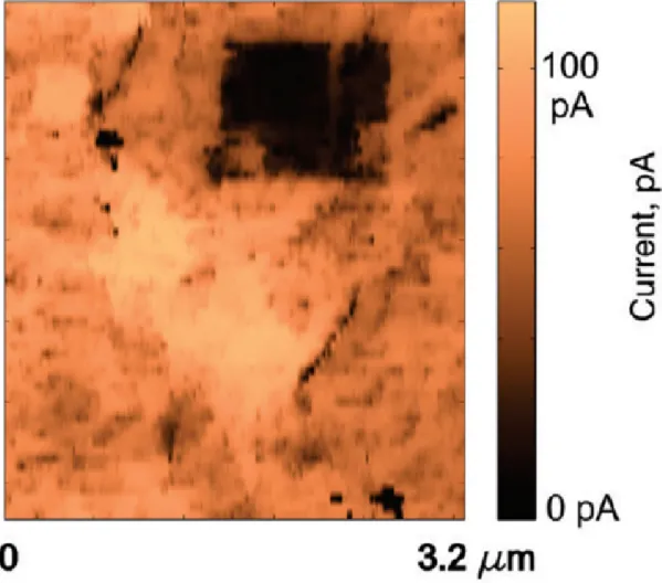
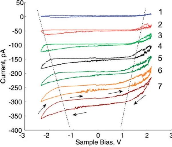
Figure 2.7: Due to the local electric field induced by a conductive atomic force microscopy tip, graphene can be locally oxidized.
Figure 2.8: Cyclic current versus voltage (I-V) measurements are performed on multilayer graphene oxide films on Au/Pd film using a Pt-coated atomic force microscope cantilever. An increase of the current at smaller bias voltage after successive (1 to 7) I-V measurements suggests a decrease in the local effective band gap. Despite a symmetric voltage sweep, a net reduction effect is observed, suggesting that oxidation rate is smaller than reduction rate at similar magnitude bias.
Figure 2.9: Tunneling current map after the first I-V measurement shows no or little surface conductivity. (d) Tunneling current map obtained after the 7th
I-V measurement shows increased current on one flake (or few flakes), suggesting whole individual flakes are reduced. Dashed red contour shows the reduced region and arrow denotes the location of the cantilever tip.
small current levels of few tens of picoamperes. Gradual decrease of the band gap during reduction is evidenced by changes in the positive and negative onsets of currents. Before and after the voltage sweeps, surface conductivity is imaged using a small bias (1100 mV), and a similar emergent heterostructured mesh of graphene/GO is seen on an individual flake (Figure 2.9 a and b). Reduction of the whole flake (or flakes, as highlighted by the red dashed line in Figure 2.9b) instead of a small spot right below the tip is possibly due to poor grounding of the topmost flake on the insulating MLGO film.
The reason for this is that the multilayer graphene oxide films are quite in-sulating and the effective resistance between the tip and the topmost flake is smaller than the effective resistance between the flake and the ground contact. Therefore, during application of the bias with the tip, whole flake is charged to a potential different than zero. The effective resistance within the flake is also smaller than the resistance between the topmost flake and underlying flakes. Therefore, the carriers injected into the flake diffuse within the flake and facilitate
Figure 2.10: (a) Multilayer graphene oxide films, which have not been subject to thermal or electrical reduction shows low surface conductivity as observed by tunneling current maps obtained with a Pt tip (10 mV bias). (b) Upon partial reduction, conductive domains are observed in the tunneling current maps. (c) Tunneling current maps of chemically or thermally reduced multilayer graphene films show plateaus of current instead of conductive spots. (d) Cyclic current-voltage measurements are performed on two-terminal devices with unreduced graphene oxide. Hysteresis and changes in the I-V curves show that graphene oxide films feature both resistive switching and capacitive charge storage. (e) Hysteresis is decreased for two-terminal devices fabricated using partially reduced graphene oxide films, and (f) no observable hysteresis is present in multilayer graphene films obtained by complete thermal reduction (150 ◦C, few minutes thermal exposure) of graphene oxide films.
the electrochemical reaction, resulting in reduction of the whole flake. In con-trast, tip-induced oxidation is performed on a relatively high conductivity film, and potentials are defined with higher spatial resolution. This is why the rectan-gle shown in Figure 2.7 is much better defined in shape than the reduced region of Figure 2.9b.
The time scales and voltages required for reduction and oxidation are also quite different; oxidation requires longer times and higher voltages. This suggests that the activation energies of reduction and oxidation are different. We assume that oxidation takes place by an electrochemical process within the water meniscus
formed between the tip and the sample, similar to tip-induced oxidation of vari-ous metals and semiconductors[39, 40, 41]. The observation that reduction takes place at very small current levels suggests that reduction is also an electrochem-ical process and not a thermal process. Oxygen coverage can be manipulated by applying electric fields in the noncontact mode as well (data not shown), suggest-ing that the electric field of the tip can also be used to manipulate the surface. Electron injection into graphene oxide is thought to facilitate the reduction, due to weakening of the bonds of negatively charge oxygen atoms with the graphene layer. The presence of states that trap electrons inside graphene oxide layers is evidenced by the charge storage effect observed in cyclic current-voltage mea-surements on two-terminal devices. A graphene oxide device with an apparently insulating surface (Figure 2.10a) shows nonzero current during a cyclic voltage sweep (Figure 2.10d).
Hysteresis observed in the I-V curves demonstrates charge storage (nonzero cur-rent at zero bias) and resistive switching (curcur-rent asymmetry and change of the shape of the forward and backward sweep curves, around -0.2 V and 0.2 V in Figure 2.10d). Upon cycling the voltage with increasing maximum voltage levels, reduction takes place, accompanied with resistive switching. Upon further reduc-tion, conductive islands begin to form on the surface similar to those observed for thermal PRGO films (Figure 2.10b). For the PRGO films, the hysteresis in the current-voltage curves is reduced (Figure 2.10e). Chemically or thermally reduced multilayer graphene film surfaces do not have conductive dots on the surface (Figure 2.10c), and they do not display charge storage or resistive switch-ing effects (Figure 2.10f). It must be noted that we were not able to observe reversible oxidation when we start with films of chemically reduced graphene. This may be due to the high conductivity of such films and resulting inability to establish significantly differing potentials within the film. The results show that electrical charge has a strong effect on the thermodynamic equilibrium of graphene/ oxygen system. In ambient atmosphere, positive charge causes oxida-tion of graphene, and negative charge enhances the reducoxida-tion of graphene oxide to graphene. Graphene oxide flakes are unstable and slowly decompose to partially reduced graphene oxide. The decomposition process is slow at room temperature. For instance, it is observed that graphene oxide suspensions start to darken in
a few months at 25 ◦C, which indicates the partial reduction of graphene oxide. However, negative charging effectively increases the free energy change (G of the decomposition reaction). Increased driving force (G) greatly enhances the rate of the reaction, and it is possible to completely reduce graphene oxide in a few seconds. Also, for the oxidation case of partially reduced graphene oxide, the reaction is not spontaneous under ambient conditions and temperature. When graphene is positively charged, the oxidation is spontaneous. The reaction rate is observed to depend on initial oxygen coverage of graphene and is slower for graphene-like films. Both graphene quantum dots are formed and oxygen cov-erage change during the electrical reduction. The equilibrium size distribution of the quantum dots can be controlled with the applied voltage. In order to de-termine the equilibrium stoichiometry and structure, the partition function must be written for the graphene/graphene oxide system, also including the electro-static energy due to the presence of excess charge. Oxygen is known to bind to graphene in a number of different configurations, resulting in different band gaps and binding energies[24]. The binding energy of individual oxygen atoms on graphene is also a function of coverage, as well as being dependent on the actual binding configuration (bond type) and presence of neighboring oxygen atoms[25]. A thorough thermodynamic analysis of the phenomenon, as observed under am-bient conditions, must take into account the myriad configurations of binding of oxygen, hydrogen, and hydroxide, in the presence of excess charge. Such an analysis must involve ab initio calculations of total energy for a large number of configurations with a large number of atoms. We do not attempt to perform such an analysis in this thesis.
Chapter 3
Tunable Ultrafast Optical
Response of Graphene Oxide
3.1
Introduction
Ultrafast dynamics and nonlinear optical response of graphene has been the sub-ject of considerable research[42, 43]. Graphene is known to exhibit wideband nonlinear saturable absorption SA. It is accepted that due to Pauli blocking, nonlinear absorption NA in graphene is not allowed.
Graphene oxide GO is an insulator, with an effective energy gap that depends on the stoichiometry[44, 25]. In GO, it was found that two-photon absorption dominate the NA for picosecond pulses, whereas for nanosecond pulses excited state absorption also influences the nonlinear response.[45], It has been previ-ously observed that, GO can be reduced controllably by annealing at below 300
◦C low-T in ambient atmosphere.[26, 27] Interruption of the annealing results in
partially reduced GO PRGO. GO has been reduced by exposing to a photographic camera flash [28], or femtosecond laser.[46], Very recently, we studied reversible electrical reduction and oxidation of GO.[47], Nanoscale inspection showed that GO islands segregate within graphene, and a two-dimensional heterostructure
the oxidation level on nonlinear optical properties of GO. We demonstrate that both electrochemically induced reversible reduction and optically induced pho-toreduction in GO result in changes in the nonlinear optical properties of GO thin films. We present the carrier dynamics and nonlinear optical properties of such films, studied by ultrafast wavelength-dependent pump-probe spectroscopy. We show that ultrafast response of GO can be tuned by both reduction procedure.
3.2
Experimental
The preparation, characterization, linear optical, and electrochromism properties of GO were very recently reported in Chapter 2. We study the electrical reduc-tion in GO in air, using multilayer GO thin films deposited on metalized glass substrates. The two terminal devices consist of thin 10 50 nm Pd/Au planar contacts, separated by 0.30.6 mm, with a thin multilayer GO film covering both contacts and in between Figure 3.1a. The degree of chemical reduction and linear absorption spectrum can be tuned by applying a fixed voltage difference to the contacts. A gradual increase in the absorption edge as a function of applied bias is observed.[47], During the cyclic voltage sweeps, it is seen that the linear optical transparency of the films change between partially opaque and transparent states. Electrochemically induced oxidation/reduction takes place within a time scale on the order of seconds for applied bias voltages of 2.5 V. We infer the thickness of the films to be 3060 nm using optical measurements, assuming the films have graphene like optical absorption during the reduced state. Wavelength-dependent pump probe measurements were performed by using Ti:sapphire laser amplifier-optical parametric amplifier system Spectra Physics, Spitfire Pro XP, TOPAS with 44 fs pulse duration and 1 KHz repetition rate. Commercial pump probe experimental setup with white light continuum probe beam Spectra Physics, He-lios was used. Experiments were performed with 400, 590, and 790 nm pump wavelengths. Pulse duration inside pump-probe experimental set up was mea-sured via cross correlation of pump and probe pulses and it was found to be around 100 fs. Positive sign of pump probe data A=T/T0 corresponds to NA whereas negative sign of A corresponds to SA in our convention.
3.3
Characterization and ultrafast optical
re-sponse
We investigate the ultrafast optical response of the films while the voltage bias is applied. A film left in the oxidized state after multiple redox cycles is char-acterized by the pump-probe technique. Figure 3.1 shows normalized change in the absorption of the white light continuum spectra, measured using 790 nm, 0.5 J pump energy with a typical pulse width of 100 fs, upon application of a time varying voltage profile shown in Figure 3.1b. Although initially SA is dominant over the whole spectrum, NA appears rapidly in a matter of seconds upon oxida-tion Figures 3.1c and 3.1d.
We attribute this to an increase in the degree of oxidation of GO, causing SA to gradually switch to NA for short probe wavelengths, possibly due to modi-fication of the band-structure of the material. The oxidation state can be con-trolled electrochemically and GO can be reduced by application of a negative bias Figure 3.1c. Even when electrochemically or thermos-optically induced partial reduction takes place, we still observe NA at longer probe wavelengths 750 nm, suggesting only a partial reduction in GO. Application of a 2.5 V bias causes the advancing of SA behavior toward longer wavelengths, suggesting the presence of a stoichiometry-dependent effective band-gap.
The ultrafast response can therefore be modified upon application of the bias. The experiments were performed with different pump wavelengths, and similar results with varying decay times and modulation depths are observed.
Figures 3.2a and 3.2c show differential absorption of probe 430780 nm with simultaneously applied pump 0.5 J, 400 nm, 44 fs for GO; without applying bias, applying 2.5 V for 5 s and applying +2.5 V for 5 s, respectively. It is clearly seen that the ultrafast optical absorption of the samples can be switched from SA to NA reversibly depending on the wavelength and degree of the reduction.
Figure 3.1: Color online schematic description of the device used in the measure-ments. (b) The applied bias voltage profile and (c) normalized differential probe transmission A as defined in text are plotted as a function of wavelength and time. Wavelength dependent switching between saturable and NA is observed upon application of the bias pump excitation energy of 0.5 J, center wavelength of 790 nm, pulse width of 44 fs. The dashed lines are guidelines for the eyes, delineating the transition wavelength between saturable and NA. (d) Differential absorption A plotted as a function of wavelength for three representative points with different bias conditions regions I, II, and III in cshowing NA and SA.
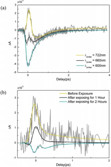
Figure 3.2: A color online differential absorption of probe at zero pump-probe delay. ac show voltage bias dependence. df Changes in the response upon high-intensity pump exposure for various durations. Similar changes are observed for electrochemical and photothermal reduction.
fs without applying bias. Figures 3.2d3.2f show differential absorption of probe 430780 nm with simultaneously applied pump for GO, without prior exposure, after exposing to pump for 1 h and for 2 h, respectively. Photo-reduction in GO takes places by exposing high intensity femtosecond pulses and this process is irreversible.
Applying high intensity femto-second pulses and negative bias causes similar effects on the differential absorption characteristics of GO. At intermediate ox-idation stoichiometry is achieved by application of a 2.5 V bias or by exposing to high intensity femtosecond pulses, if the probe wavelength is chosen near the SA/NA transition, NA signal starts appearing within the SA signal region Figs. 3.3a and 3.3b. For example, as seen in Figure 3.3a, the NA peak appears within 100200 fs of the arrival of the pump pulse. Such a time scale between the carrier-carrier scattering and carrier-carrierphonon scattering causes the NA process disappears in a very short time, leaving the tail of carrierphonon scattering visible. In a simplistic view, it can be assumed that the simultaneous appearance of SA and NA is the result of isolated regions of the material acting as graphene and GO. The optical response is averaged over the 300 m diameter illumination spot-size and the material behaves like an effective material with multiple components. In such a case, the persistence of NA for a variety of pump wavelengths even when the pump photon energy is less than the apparent absorption edge of GO, requires that multiphoton absorption or absorption of the probe through inter-mediate states must be present.
Previous reports on observations of simultaneous presence of SA and NA in graphene offered an explanation in terms of doping of the graphene layers. Switch-ing as a function of the probe wavelength from saturation to NA was observed around 1.78 m for doped epitaxial graphene on SiC[48]. The NA of the probe seen at longer wavelengths and saturation seen at shorter wavelengths were at-tributed to the shifting in the Fermi level due to doping. As molecules bind to the surface of the graphene, depending on the molecule and the binding location graphene experiences a charge transfer as a donor and acceptor, thus changing
Figure 3.3: Color online (a) temporal behavior of the saturated and NA responses at different probe wavelengths after applying bias voltage. (b) Temporal behavior of the saturated and NA responses at 750 nm probe wavelength depending on the exposure time to pump pump excitation energy of 5 J, center wavelength of 790 nm, pulse width of 44 fs.
the Fermi level, carrier density, and electrical resistance of graphene[49]. In addi-tion, the band structure itself may be modified depending on the type, locaaddi-tion, and density of the binding species[25]. In our case, the observed NA/saturation behavior may be attributed to such modifications of Fermi level or band structure upon electrochemical stimulus. The zero crossing wavelengths can be tuned from 550 nm to beyond 800 nm our probe range. Although the exact origin of the electrochromic effects in the ultrafast regime is disputable, due to the SA/NA cancellation effect, for carefully chosen pump-probe wavelength and degree of re-duction combinations, the nonlinear response of graphene can be tuned to display a very fast 100 fs effective NA decay time constant.
Chapter 4
Surface-Enhanced Raman
Spectroscopy of Volatile Organic
Compounds
4.1
Introduction
Raman spectroscopy is a valuable tool commonly used in the characterization of chemical substances. During the interaction of light with matter, small (≈ 10−7) percentage of photons scatters in-elastically. Photons interact with the vibrational states of the material and an energy exchange occurs between them. During scattering, energy transfer between photons and vibrational states is called Raman Scattering and measuring the energy change of the scattered photon is Raman Spectroscopy. It is possible to identify materials by using their Raman spectra because each material has its own vibration energy states. However, it is hard to characterize materials with low concentration with Raman Spectroscopy due to low statistics of this physical phenomenon. Plasmonic nanostructures en-hance absorption and increase the number of inelastic scattered photons [50, 51]. Therefore, Raman signal increases when samples placed on plasmonic surfaces.
makes it possible to detect and characterize chemicals with low concentration also [52, 53].
Volatile organic compounds (VOCs) are organic molecules that have high vapor pressure at room temperature. VOCs evaporate and condense onto substances. There are variety of VOC sources such as paints, coatings, chlorofluorocarbons and cleaning products. VOCs are also important molecules for eviroment . De-tection of VOCs has several practical applications such as explosive deDe-tection, opto-electronic nose for drugs and breathe analysis. In this thesis, we have fo-cused on detection VOCs by using SERS.
4.2
Chemical synthesis, fabrication and
charac-terization of SERS substrates
We have used a chemical synthesis method to fabricate SERS substrates. Due to the high enhancement factor used in SERS, we needed a process with minimum residual chemicals. Therefore, we have used a synthesis method developed for conductive ink application [54]. The chemical reaction is shown below. We have prepared a paste and drop cast the solution on a clean glass substrate. As shown in the equation, the included chemicals decompose spontaneously. After room temperature drying of the silver based paste, all the residuals evaporate and a rough silver layer was plated on the surface. The final products are solid silver and volatile compounds. After 6 hours drying of the film, we have measured the SERS performance. We observed that enhancement factor of the substrate is adequate enough; however structural uniformity is not enough for the applications that are aiming to do.
We have decided to do the rest of the experiments with a more simple, uniform and clean technique to fabricate SERS substrates. In this technique, we have evaporated thin films of silver onto glass substrates. Nanoparticles formed on the surface because of the surface tension of silver. The particle size depends on the thickness of the evaporated film. Additionally, the formed nanoparticles are close to each other as shown in the Figure 4.1. Because of the short distance between
Figure 4.1: Image of 3nm silver coated glass slide.
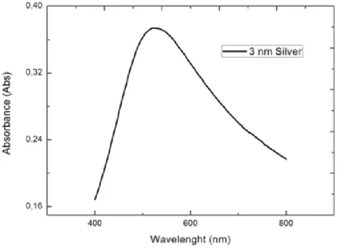
particles, they behave like a coupled waveguide that enhances the absorption and forms hot points. Our Raman microscope uses a laser with a wavelength of 532 nm for excitation. Therefore, we have optimized maximum absorption of the silver film to be around 532nm. Figure 4.2 shows the wavelength vs absorbance of 3nm thickness silver film on glass. Silver film has a good match with laser wavelength as shown in the Figure 4.2. However, the most important drawback of silver is quick oxidation which decreases repeatability of the experiments. In the Figure 4.3, we have measured absorbance change with time. Experiments should be done with newly prepared samples to make repeatable experiments,. Addition to its oxidation problem, substrates are very sensitive to heat also. Laser radiation and elevated temperatures cause nanoparticles to accumulate. In the Figure 4.4, we have measured the effect of heat treatment on silver films. Due to increased mobility, average particle size has increased and absorbance shifted through red.
4.3
Single molecule sensing with SERS
Plasmonically active substrates have been fabricated for SERS experiments. We have fabricated metallic nanostructures by using different techniques including
Figure 4.3: Absorbance vs wavelength of 3nm silver coated glass slide just after fabrication and 1 week after fabrication.
chemical synthesis and evaporation. At the start of the experiments, we have recognized an interesting phenomenon. On blank SERS substrates and with low laser power, we observed blinking in Raman signal. The blinking is independent from technique used in the fabrication of SERS substrate. Raman spectra mea-sured during blinking were similar and coming from unknown substances possible originated from ambient atmosphere. We recognized that those fluctuations in Raman spectra were coming from VOCs molecules. The reason of the blinking is surface diffusion causes VOCs to enter and exit hot spot.
Previously, similar fluctuations in Raman spectra have been observed [52, 55, 56]. Those fluctuations regarded as single molecule SERS spectra. We have also ob-served similar SERS spectra in ambient atmosphere with high quality factor. However, Raman spectra of blank substrates are very complicated and hard to manipulate manually. The main reason is Raman spectrum of a substance on a SERS substrate is different than its bulk Raman spectrum [51]. And SERS spectra could depend on the molecular orientation. We have developed an
analy-Figure 4.4: Absorbance vs wavelength of 3nm silver coated glass slide and after heat treatment.
algorithm to identify VOCs.
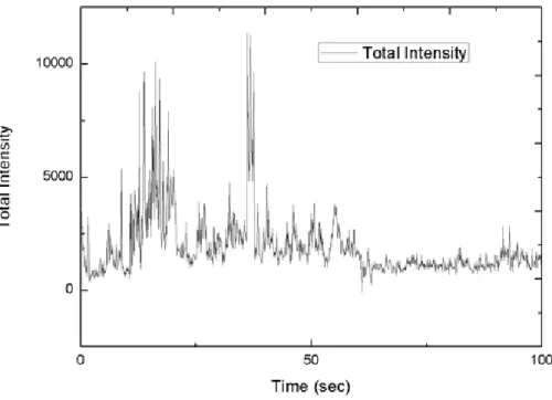
We have made experiments to reveal the mechanism and to identify airborne molecules. In the Figure 4.5, a common time vs total Raman intensity graph of a black SERS substrate is shown. We have covered silver surface with a monolayer of 4-MBA(4-Mercaptobenzoic acid) to isolate silver from ambient atmosphere. As shown in the Figure 4.6, we did not see any blinking as shown in the graph when the surface is covered by a self-assembled monolayer. This supports that blinking is originated from the free molecules diffusing on the substrate surface. Interactions of the molecules with the SERS substrate could change their Raman spectra also. 4-MBA acid physically binds to the silver surface due to its thiol group. We observed that Raman spectra shifted when 4-MBA interacts with the surface. In the Figure 4.7, Raman spectrum shifted to red as predicted by the simulation results [57] due to physical interaction of 4-MBA with the surface dur-ing its surface diffusion. This experiment showed that, it is possible to measure real time molecule-surface interactions by using SERS spectra.
Raman spectra also include florescence and scattered photons other than Ra-man. Raman signals of diffusing molecules should be isolated from total signal to identify unknown VOCs. Therefore, we have taken derivative of the Raman spectra to see the changes made by hoping molecules. In the Figures 4.8a and 4.8b, original vs derivative times series of total Raman signal is shown.
To identify Raman spectra of VOCs, we have modified the algorithm to find the most abundant spectra. The result was interesting. We have identified the spec-trum by using Raman databases and it was identified as 3-(4-tert-Butylphenyl)-2-methylpropanal. It is kind of a fragrance molecule that is commonly used in cleaning agents. We traced the chemical and found that the laboratory was cleaned with a product includes 3-(4-tert-Butylphenyl)-2-methylpropanal which proves we have built an artificial nose can detect fragrances. We purified the fragrance molecule and dissolved it in an organic solvent to make controlled ex-periments. However, no matter how high the vapor pressure was, we could not see a linear increase in the Raman signal; i.e, the signal could not be saturated.
Figure 4.6: Total intensity of Raman signal vs time of a SERS substrate covered by 4-MBA monolayer.
Figure 4.7: SERS spectra of 4-MBA. When 4-MBA goes into physical interaction with the silver surface, total spectra shifts to the left.
Figure 4.8: (b) Time vs total intensity Raman signal of blank substrate. (a) Time vs differential of Raman signal. (c) Raman spectrum at the peak shown by black arrow.
Figure 4.9: Microscope image of fragrance thin film on SERS substrate. (a) is unexposed film, (b) Laser light induces a repelling force, (c) Laser is closed and thin film covered the surface again.
We have dip-coated substrate surface with purified fragrance to measure the Ra-man spectrum of the bulk sample. We observed that the surface repels the fra-grance thin film with a light driven force (Figure 4.9). When the light is on, a hole appears on the film. The change on thin film was reversible. Based on these results, light driven force repels excess amount of chemicals from surface and prevents saturation. This phenomenon enables us to characterize a mixture of chemicals at the same time which is not possible in mammalian olfactory system and most of the artificial noses.
We have done experiments to develop this technique to detect explosive vapour from air. However, identifying molecules from SERS spectra is difficult because of the difference between bulk vs SERS spectra. We need to know exact SERS spectra of the compounds to manipulate their spectrum from total signal. We con-taminated air with well-known materials to measure SERS fingerprints of them. Different materials were encapsulated with SERS substrates. In the encapsula-tion, due to vapor pressure of the materials, volatile materials are supposed to evaporate and condense onto SERS substrates which allowed us to measure SERS fingerprints during surface diffusion.
We have achieved to measure SERS fingerprints of some materials by taking the average of total time series of encapsulated substrates. The SERS fingerprints of the materials are shown in the Figures 4.10, 4.11 and 4.12. We have applied a
Figure 4.10: Average surface-enhanced Raman spectrum of TNT.
filter to Raman spectra which only multiplication of the major peak positions of average SERS spectrum of TNT is shown. This means that when a TNT enters to the hot spot, it should give a Raman spectrum similar to the previously mea-sured SERS fingerprint of TNT, consequently a peak should be observed in the filtered times series as shown in the Figure 4.13. With this technique, it is possi-ble to count TNT molecules that came to the hot spot. In the Figure 4.14, SERS spectra of the highest peak in Figure 4.13 and SERS fingerprint of TNT molecule is compared. Similarity between the fingerprint and actual spectra proves that our filters are working correctly.
To sum up, we have demonstrated single molecule sensing of airborne molecules with Raman spectroscopy. Sensing mechanism is based on Raman scattering of hoping volatile organic compounds on surface-enhanced Raman spectroscopy sub-strates. The fabricated sensor can distinguish even residual fragrance molecules
Figure 4.12: Average surface-enhanced Raman spectrum of Lauric acid.
Figure 4.13: Time series of a filtered Raman spectra of a SERS substrate. A TNT sample was placed near SERS substrate. Total Raman signal wavelength filtered with TNT peak positions obtained from average surface-enhanced Raman spectrum of TNT. The peak at approximately 35th sec. is assumed to be a TNT
Figure 4.14: Captured Raman signal from blank SERS substrate vs SERS finger-print of TNT. A TNT sample was placed near SERS substrate.
that excess amount of target molecules could not saturate the sensor contrary to mammalian olfactory system. Experiments revealed that sensor surface repels excess molecules with a light driven force. This phenomenon could be observed on sensor surface dip-coated with target molecules. We also showed that, it is possible to track target molecules by using SERS fingerprints.
4.4
Portable Raman microscope
We have design a portable Raman microscope that is specifically design for blink-ing phenomena (Figure.4.15 and 4.16). The device could be used for point of care and portable detection of VOCs. The device was 3D printed and assembled with the required optical elements (Figure 4.17). The device is using smart-phones to read-out Raman Signal. A built-in grating was placed between the image plane and imaging lens. When blinking occurs, light disperses into a line that could be read out as fluorescence and Raman spectrum. A constant current driven 532 nm DPSS (Diode-Pumped-Solid-State) laser used as an excitation source. An excitation filter was used to eliminate pump diode emission. A dichroic mirror, an aspherical lens and an emission filter were used in the optical path.