www.nature.com/scientificreports
Chemical Visualization of a GaN
p-n junction by XPS
Deniz Caliskan1, Hikmet Sezen2, Ekmel Ozbay1 & Sefik Suzer2
We report on an operando XPS investigation of a GaN diode, by recording the Ga2p3/2 peak position
under both forward and reverse bias. Areal maps of the peak positions under reverse bias are completely decoupled with respect to doped regions and allow a novel chemical visualization of the p-n junction in a 2-D fashion. Other electrical properties of the device, such as leakage current, resistivity of the domains are also tapped via recording line-scan spectra. Application of a triangular voltage excitation enables probing photoresponse of the device.
The diode or the p-n junction is the single most important functional and central element of almost all of the electronic and optoelectronic devices1. Therefore, its design, fabrication as well as characterization
are all important issues. Traditionally, elaborate but mostly electrical based techniques have been utilized for detection and/or characterization of a device which usually includes a number of different electrical units, such as junctions, transistors, etc. On the other hand, powerful analytical techniques are increas-ingly being used for probing chemical and physical together with electrical properties of materials and devices in much smaller size and under realistic operating conditions. Scanning Electron microscopy (SEM) is one of these methods, where imaging with submicron lateral resolution is an added advantage. This was first shown by Chang and Nixon reporting on observation of a significant change in the second-ary electron yield across a p-n junction2. Kaetsner et al.3 used SEM to demonstrate a direct observation
of the potential variations inside a 90-nm GaAs channel4, and Li et al. in carbon nanotubes5. Electrical
biasing together with SEM mapping is a recent elaboration of the technique providing direct imaging of the p-n junction, including its depletion width, made up from GaInP/GaAs4 heterojunctions, and in GaN
nanowires5–7. Cathodoluminescence in a scanning transmission microscope (CL-STEM)8 and conductive
atomic force microscopy are other techniques used to characterize the p-n junction in GaN nanorods9
and porous GaN based LEDs10. Formation and characterization of p-n junctions in photodiodes and
photovoltaics have also been heavily investigated using a combination of electrical and optical analyses tools10–17.
However, all of these techniques provide very limited chemical information, if any. In this respect, electron spectroscopic techniques, such as Auger Electron Spectroscopy (AES) and X-Ray Photoelectron Spectroscopy (XPS) have the ability to reflect the electrical potential of the medium surrounding the probed atom, created intentionally or not18–31, and render them even more powerful for investigating
materials and especially device performances under operational conditions, the so-named in-operando AES or XPS. Use of AES for probing the electrical potential variations across a working device was first reported three decades ago, but the technique has not been pursued due to its limited chemical specificity32–36. Numerous successful reports have also appeared for probing potential variations across
a p-n junction device using PEEM (photoemission electron microscopy), a variant of electron spectros-copy, but again it also has limited chemical specificity31,37–41. Exciting applications towards investigating
devices under more realistic operational conditions are now being reported as a consequence of the recent advances in ambient-pressure XPS (APXPS)42–45. In parallel, recent advances in commercial XPS
instrumentation, like micro-focusing and parallel detection systems, have also provided new possibilities to record XPS data with higher lateral resolution and good statistics in reasonable measurement times46. 1Nanotechnology Research Center, Department of Electrical and Electronics Engineering and Department of Physics, Bilkent University, 06800, Ankara, Turkey. 2Department of Chemistry, Bilkent University, 06800 Ankara, Turkey. Correspondence and requests for materials should be addressed to S.S. ([email protected]) Received: 07 April 2015
Accepted: 17 August 2015 Published: 11 September 2015
OPEN
www.nature.com/scientificreports/
In one of our recent publications, we presented an XPS investigation of a CdS-based photoresistor, taking advantage of these instrumentation capabilities, and under working conditions for the device47.
The electrical potential variations across the device were mapped by recording the binding energy posi-tions under an applied + 6 V d.c. bias across the electrodes, and with and without laser illumination at different wavelengths. Variations in the Cd3d5/2 peak positions were used to extract electrical parameters
and detect the presence of morphological defects affecting the performance of the device in a chemically specific fashion. A similar study was also presented for a CVD grown resistive graphene layer between two gold electrodes, and by imposing current flow through the device. Such a procedure allowed us to detect the presence of morphological defects and cracks when the graphene layer was subjected to a mild oxidation48. Furthering that study, we also reported on an investigation where gate-tunable
pho-toemission was recorded of a graphene transistor, for the graphene as well as the Si3N4 substrate layers49.
Another one of our publication reported investigation of the p-n junction of a commercial Si-diode during its operation under forward and reverse bias50. The present work extends such an investigation to
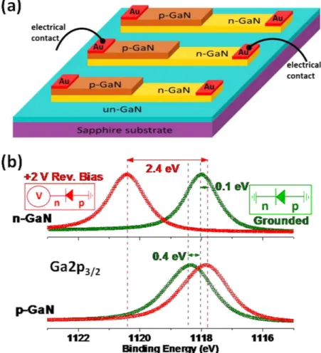
the entire surface (2 dimensional) of a GaN device consisting of three parallel diodes, as shown in Fig. 1a, but only one is operated at a time. GaN is a wide band-gap compound semiconductor with superior electronic and optoelectronic properties utilized in numerous devices for light emitting diodes, sensors and transistors for high power and high frequency applications51. Therefore, better understanding of
physical and chemical properties of devices based on GaN are expected to pave ways to technological advancement in numerous applications.
Results
Figure 1b depicts the Ga 2p3/2 peak of the p- and n- regions of the middle device recorded under + 2 V
bias as well as when grounded. For an undoped GaN (un-GaN), the tabulated binding energy of the Ga2p3/2 is 1117.9 eV, there is already a small binding energy difference of 0.4 eV between p- and n-
regions when the XPS data is recorded in the conventional (both electrodes grounded) fashion, due to differences in their Femi-level pinning at the surface, in accordance with published data51–55, which was
discussed in detail in our previous work56,57. The more dramatic change between the p- and n- regions
materializes when recorded under + 2 V reverse bias, upon which the peaks in the n- and p-regions
Figure 1. (a) Schematic of the device and its electrical contacts. (b) XPS spectra. Ga 2p3/2 peak recorded
www.nature.com/scientificreports/
exhibit 2.4 eV relative binding energy difference, due to charge built-up across the junction. We have also measured the shift in the Au4f7.2 peak of the gold electrodes connected to yield only 2.02 eV
reproduc-ing faithfully the bias voltage within the experimental uncertainty of 50 meV. This findreproduc-ing validates the accuracy and the precision of our measurements, and also confirms the absence of any significant contact resistance(s) within the entire experimental set-up. The persistence of the additional and opposite sign 0.4 eV difference between the n- and p-regions, even under 2 V bias is remarkable.
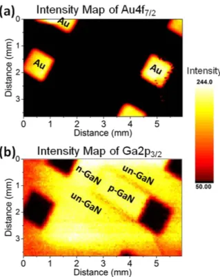
Figure 2 displays areal intensity maps of the Au4f7.2 and the Ga2p3/2 peaks recorded in the snap-shot
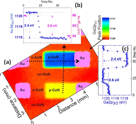
mode. The intensity variations of the Ga peak between various regions are indistinguishable except at the intersection of the un-GaN and the p-GaN regions. In Fig. 3, the areal map of the measured binding energy positions of the Ga2p3/2 peak under + 2 V reverse bias is displayed, where now the differences
are transformed into the voltage space and amplified. As shown in the inset, the two doped regions display 2.4 eV difference in the binding energy position under + 2 V reverse bias, traversing across the gold electrodes. Traversing in the middle and perpendicularly crosses the side-walls of the intersection of the un-GaN and the grounded p-GaN twice. Interestingly although an equivalent of the full junction potential of 2.4 eV is measurable at the side-walls of the un- and p- intersection (see Fig. 3b), only 0.6 eV voltage drop is measured between the un- and the floating p- regions of the neighboring diode (Fig. 3c), indicative of a certain cross-talk among the diodes. Unfortunately, our spatial resolution of > 50 μ m does not permit assessing the depletion length or other similar properties of the junction4,5, except for stating
that the depletion length is smaller than 50 μ m. Note also that the measured binding energy difference in the Au4f7.2 peak of the two gold electrodes is still consistently 2.0 eV, as is also indicated in the inset,
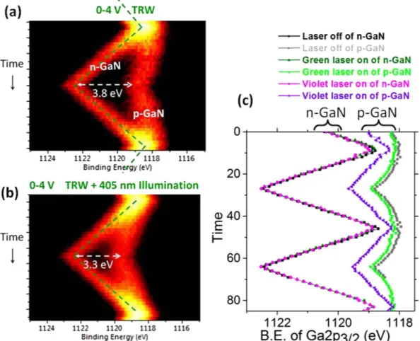
and we reiterate that each GaN region and their interfaces exhibit different binding energy shifts. Further XPS analyses of the junction were carried out by imposing a slow time-varying triangular voltage stimuli of 0–4 V, and also by exposing the sample to light illumination with different colors. In Fig. 4a, the time variations of the Ga2p3/2 peak of a 200 μ m spot is shown, where the spot is positioned
on the junction covering both the n- and p- sides almost equally. When the device is forward biased, the Ga2p3/2 peaks of the n- and p-regions overlap, but start splitting apart into two components when
the device enters the rectifying mode. The splitting increases up to the turning point with a reproducible symmetry. Note, however, the rectification is not all that perfect and small but a measurable slope is also displayed by the p-component, due to unwanted leakage current, which is also present in the I–V characteristics of the device, as shown in the Supplementary Information (SI) section as Figure S1. In addition, as shown in Fig. 4b,c, whereas illumination by green laser does not alter the performance of the p-n junction, the performance is degraded further under violet light illumination, which leads us to postulate the presence of a parallel resistor (Rp) controlled by violet light, i.e. a photoresistor. A simple
equivalent circuit can now be formulated, which is given in Fig. 5 and also in the SI section, by assum-ing the presence of two series resistor in the n- and p- regions and a parallel (photo) resistor across the
Figure 2. XPS Intensity Maps. Areal maps of the intensity of the Au4f7/2 and Ga2p3/2 peaks derived from
www.nature.com/scientificreports/
junction, in order to account for this realistic performance of the device, at least for its d.c. and/or low frequency response11. In principle both the green 532 nm (2.3 eV) and the violet 405 nm light (3.1 eV)
should not have contributed to the band to band photoconductivity of GaN with a band-gap of 3.4 eV54.
Hence, the presence of deep traps and defects must be causing such changes, which was also reported in our previous studies56,57.
Consistency and symmetry checks of our analyses are also performed by recording normal scanned spectra in the form of line-scans, with higher energy resolution and better accuracy as shown in Fig. 5a across the gold electrodes, by application of + 4 and − 4 V reverse bias geometries (as shown in Figure S2 of the SI section), and recording both the Ga2p3/2 as well as the Au4f7.2 peaks (not shown). Going across
the device a total of 4.4 eV voltage drop is measured in the Ga3/2 peak, whereas only 4.0 eV in the Au one,
consistent with the persistent 0.4 eV Fermi-level difference between the n- and p-GaN regions. In accord-ance with the results of the triangular excitation, only 3.8 V of the applied reverse bias develops across the junction, and the remaining 0.6 V through the p-region only. Knowing that the p-GaN is more resis-tive56,57, we can estimate the value of the series resistor (R
p) as ~0.9 kΩ , in the p-region, and an almost
negligible one for the n-one, using the equivalent circuit model, and the 700 μ A leakage current extracted from Figure S1 of the SI section. Noting that under violet light illumination, the voltage drop across the junction drops down to 3.3 eV (see Fig. 4b,c), and assuming that the Rp does not change significantly,
we can now estimate that an additional ~580 μ A leakage current (totaling to ~1.28 mA) is introduced by the violet light illumination. Details of the computations are given in the SI section. Admittedly, this is a grossly oversimplified approach, since band-bending and other processes, impurities, defects, etc., are expected to contribute significantly to the overall voltage variations in a working device. On the other hand, our strategy offers a pivotal experimental tool for sorting out such effects, and calls for further experimental as well as theoretical and/or modeling work.
In summary, many of the electrical properties of a p-n junction can be probed and visualized in a chemically specific fashion during its realistic operating conditions (in-operando) by recording XPS data, while imposing different forms of voltage and optical stimuli. This simple and novel experimental methodology opens up completely new avenues for utilization of the 5-decades old but powerful XPS technique for chemically specific electrical properties of both materials and devices with respect to the otherwise impossible performance- and/or failure-analyses.
Figure 3. XPS Binding Energy Map. (a) Areal map of the variations in the binding energy of Ga2p3/2
recorded under + 2 V reverse bias. (b) The peak positions of Au4f7/2 and Ga2p3/2 peaks along the lines
www.nature.com/scientificreports/
Methods
Sample Preparation and Device Fabrication. The epitaxial structure growth was started with des-orption cleaning of C plane sapphire substrate at 1100 °C under H2 flow. Low temperature AlN
nuclea-tion layer was grown at 50 mbar reactor pressure and 790 °C substrate temperature. Following the growth of 700 nm thick ud-GaN layer at 200 mbar and 1050 °C SiH4 source was opened at the same growth
condition to provide n- type doping. After 750 nm growth n-GaN layer temperature decreased to 980 °C
Figure 4. XPS Measuerements under 0–4 V Triangular Bias. Ga2p3/2 peak recorded under 0–4 V triangular
excitation at the junction. (a) Without illumination. (b) Under Viloet Light Illumination. (c) Derived peaks positions.
Figure 5. XPS line scans. (a) Ga2p3/2 peak recorded across the junction in the line scan mode under + 4
www.nature.com/scientificreports/
and Cp2Mg was introduced to the reactor for p- doping of 350 nm thick p-GaN layer. Following the
growth, wafer was annealed at 800 °C for 10 min in order to activate Mg impurities. Device fabrication was started with photolitograhy for p-GaN mesa etching. Etching process was performed with 800 W ICP power and 100 W RF power at 0.4 Pa reactor pressure using BCl3 (20 sccm)/Cl2 (25 sccm)/Ar (10 sccm)
gases. After 700 nm etching a second photolitograhy is performed for a wider area of device mesa and etched for a total etch dept of 1.4 μ m, reaching the ud-GaN layer. Ti (15 nm)/Al (40 nm)/Ni (40 nm)/ Au (40 nm) metals were e-beam deposited on photolitographically defined n-type ohmic contacts and annealed at 850 °C for 30 s in the forming gas atmosphere. Similarly Ni (15 nm)/Au (1500 nm) metals were used to form p-type ohmic contacts and annealed at 800 °C for 30 s. The I–V characteristics of the fabricated device is shown in Figure S1 of the SI section.
XPS Measurements. A Thermo Fisher K-Alpha electron spectrometer with monochromatic AlKα X-rays was used for the XPS analyses. The instrument is modified to allow imposition of an external volt-age bias across the sample during data acquisition47–50. For normal scans an X-ray beam size of 400 μ m
was used, but for the rest of the data presented in this work a 50 μ m-diameter X-ray spot size was used both in recording the mapped regions as well as the line scans with 50 μ m steps in between data points. A 50 mW violet at 405 nm (3.1 eV) and green at 532 nm (2.3 eV) solid states lasers in continuous wave mode are used for photoillumination.
References
1. Sze, S. M. & Ng, K. K. Physics of semiconductor devices 3rd edn (John Wiley & Sons, 2007).
2. Chang, T. H. P. & Nixon, W. C. Electron beam induced potential contrast on unbiased planar transistors. Solid State Electron. 10, 701–704 (1967).
3. Kaestner, B., Schönjahn, C. & Humphreys, C. J. Mapping the potential within a nanoscale undoped GaAs region using a scanning electron microscope. Appl. Phys. Lett. 84, 2109–2111 (2004).
4. Heath, J. T., Jiang, C.-S. & Al-Jassim, M. M. Measurement of semiconductor surface potential using the scanning electron microscope. J. Appl. Phys. 111, 046103 (2012).
5. Li, J. et al. Direct Identification of Metallic and Semiconducting Single-Walled Carbon Nanotubes in Scanning Electron Microscopy. Nano Lett. 12, 4095–4101 (2012).
6. Lu, Y.-J. et al. Dynamic Visualization of Axial p–n Junctions in Single Gallium Nitride Nanorods under Electrical Bias. ACS Nano 7, 7640–7647 (2013).
7. Tchoulfian, P. et al. Direct Imaging of p–n Junction in Core–Shell GaN Wires. Nano Lett. 14, 3491–3498 (2014).
8. Zhou, X., Lu, M.-Y., Lu, Y.-J., Gwo, S. & Gradečak, S. Correlation of doping, structure, and carrier dynamics in a single GaN nanorod. Appl. Phys. Lett. 102, 253104 (2013).
9. Deb, P. et al. GaN Nanorod Schottky and p− n Junction Diodes. Nano Lett. 6, 2893–2898 (2006).
10. Bilousov, O. V. et al. Fully Porous GaN p–n Junction Diodes Fabricated by Chemical Vapor Deposition. ACS Appl. Mater.
Interfaces 6, 17954–17964 (2014).
11. Buscema, M., Groenendijk, D. J., Steele, G. A., van der Zant, H. S. J. & Castellanos-Gomez, A. Photovoltaic effect in few-layer black phosphorus PN junctions defined by local electrostatic gating. Nat. Commun. 5, 4651 (2014).
12. Choi, J.-H. et al. Complete gate control of supercurrent in graphene p–n junctions. Nat. Commun. 4, 2525 (2013).
13. Gabor, N. M., Zhong, Z., Bosnick, K., Park, J. & McEuen, P. L. Extremely Efficient Multiple Electron-Hole Pair Generation in Carbon Nanotube Photodiodes. Science 325, 1367–1371 (2009).
14. Pospischil, A., Furchi, M. M. & Mueller, T. Solar-energy conversion and light emission in an atomic monolayer p-n diode. Nat.
Nanotechnol. 9, 257–261 (2014).
15. Yan, K. et al. Modulation-doped growth of mosaic graphene with single-crystalline p–n junctions for efficient photocurrent generation. Nat. Commun. 3, 1280 (2012).
16. Zhang, Y. J., Ye, J. T., Yomogida, Y., Takenobu, T. & Iwasa, Y. Formation of a Stable p–n Junction in a Liquid-Gated MoS2 Ambipolar Transistor. Nano Lett. 13, 3023–3028 (2013).
17. Baugher, B. W. H., Churchill, H. O. H., Yang, Y. & Jarillo-Herrero, P. Optoelectronic devices based on electrically tunable p-n diodes in a monolayer dichalcogenide. Nat. Nanotechnol. 9, 262–267 (2014).
18. Bozzini, B. et al. Microscale Evolution of Surface Chemistry and Morphology of the Key Components in Operating Hydrocarbon-Fuelled SOFCs. J. Phys. Chem. C 116, 23188–23193 (2012).
19. Bozzini, B. et al. An in Situ Synchrotron-Based Soft X-ray Microscopy Investigation of Ni Electrodeposition in a Thin-Layer Cell.
J. Phys. Chem. C 113, 9783–9787 (2009).
20. Buller, R. et al. (Pb1–xCdx)S Nanoparticles Embedded in a Conjugated Organic Matrix, as Studied by Photoluminescence and Light-Induced X-ray Photoelectron Spectroscopy. Adv. Funct. Mater. 12, 713–718 (2002).
21. Cohen, H., Maoz, R. & Sagiv, J. Transient Charge Accumulation in a Capacitive Self-Assembled Monolayer. Nano Lett. 6, 2462–2466 (2006).
22. Cohen, H., Sarkar, S. K. & Hodes, G. Chemically Resolved Photovoltage Measurements in CdSe Nanoparticle Films†. J. Phys.
Chem. B 110, 25508–25513 (2006).
23. Gregoratti, L., Mentes, T. O., Locatelli, A. & Kiskinova, M. Beam-induced effects in soft X-ray photoelectron emission microscopy experiments. J. Electron. Spectrosc. Relat. Phenom. 170, 13–18 (2009).
24. Itzhaik, Y., Hodes, G. & Cohen, H. Band Alignment and Internal Field Mapping in Solar Cells. J. Phys. Chem. Lett. 2, 2872–2876 (2011).
25. Kolmakov, A. et al. Spectromicroscopy for Addressing the Surface and Electron Transport Properties of Individual 1-D Nanostructures and Their Networks. ACS Nano 2, 1993–2000 (2008).
26. Mentovich, E., Belgorodsky, B., Gozin, M., Richter, S. & Cohen, H. Doped Biomolecules in Miniaturized Electric Junctions. J.
Am. Chem. Soc. 134, 8468–8473 (2012).
27. Phaneuf, R. J. et al. Imaging the variation in band bending across a silicon pn junction surface using spectromicroscopy. J. Appl.
Phys. 88, 863–868 (2000).
28. Samokhvalov, A. et al. Charge Transfer between a Gold Substrate and CdS Nanoparticles Assembled in Hybrid Organic− Inorganic Films. J. Phys. Chem. B 107, 4245–4252 (2003).
29. Sarkar, S. K., Hodes, G., Kronik, L. & Cohen, H. Defect-Dominated Charge Transport in Si-Supported CdSe Nanoparticle Films.
www.nature.com/scientificreports/
30. Shabtai, K., Rubinstein, I., Cohen, S. R. & Cohen, H. High-Resolution Lateral Differentiation Using a Macroscopic Probe: XPS of Organic Monolayers on Composite Au− SiO2 Surfaces. J. Am. Chem. Soc. 122, 4959–4962 (2000).
31. Thißen, A. et al. Experimental routes to in situ characterization of the electronic structure and chemical composition of cathode materials for lithium ion batteries during lithium intercalation and deintercalation using photoelectron spectroscopy and related techniques. Ionics 15, 393–403 (2009).
32. Comizzoli, R. B. & Opila, R. L. Electrical conduction mechanism in semi‐insulating polycrystalline silicon films. J. Appl. Phys. 61, 261–270 (1987).
33. Opila, R., Marchut, L. & Hollenhorst, J. Measurement of the surface electrical potential in a planar avalanche photodiode near breakdown. J. Electrochem. Soc. 137, 703–705 (1990).
34. Opila, R. L. Electron spectroscopies for simultaneous chemical and electrical analysis. Appl. Surf. Sci. 256, 1313–1315 (2009). 35. Pantel, R. Auger voltage contrast depth profiling of shallow p‐n junctions. Appl. Phys. Lett. 43, 650–652 (1983).
36. Patterson, J. M. & Smith, M. C. A Non Contact Voltage Measurement Technique using Auger Spectroscopy. Reliability Phys. Symp., 1983. 21st Annual, Phoenix. New York: IEEE (1983, April).
37. Giesen, M., Phaneuf, R. J., Williams, E. D., Einstein, T. L. & Ibach, H. Characterization of p-n junctions and surface-states on silicon devices by photoemission electron microscopy. Appl. Phys. A 64, 423–430 (1997).
38. Weinelt, M. et al. Electronic structure and electron dynamics at Si(100). Appl. Phys. A 80, 995–1003 (2005).
39. Frank, L. et al. The origin of contrast in the imaging of doped areas in silicon by slow electrons. J. Appl. Phys. 100, 093712 (2006). 40. Barrett, N., Zagonel, L. F., Renault, O. & Bailly, A. Spatially resolved, energy-filtered imaging of core level and valence band
photoemission of highly p and n doped silicon patterns. J. Phys.: Condens. Matter 21, 314015 (2009).
41. Lavayssière, M., Escher, M., Renault, O., Mariolle, D. & Barrett, N. Electrical and physical topography in energy-filtered photoelectron emission microscopy of two-dimensional silicon pn junctions. J. Electron. Spectrosc. Relat. Phenom. 186, 30–38 (2013).
42. Bluhm, H. Photoelectron spectroscopy of surfaces under humid conditions. J. Electron. Spectrosc. Relat. Phenom. 177, 71–84 (2010).
43. El Gabaly, F. et al. Measuring individual overpotentials in an operating solid-oxide electrochemical cell. PCCP 12, 12138–12145 (2010).
44. Ghosal, S. et al. Electron Spectroscopy of Aqueous Solution Interfaces Reveals Surface Enhancement of Halides. Science 307, 563–566 (2005).
45. Zhang, C. et al. Measuring fundamental properties in operating solid oxide electrochemical cells by using in situ X-ray photoelectron spectroscopy. Nat. Mater. 9, 944–949 (2010).
46. Pelissier, B. et al. Parallel angle resolved XPS investigations on 12in. wafers for the study of W and WSix oxidation in air.
Microelectron. Eng. 85, 1882–1887 (2008).
47. Sezen, H., Rockett, A. A. & Suzer, S. XPS Investigation of a CdS-Based Photoresistor under Working Conditions: Operando–XPS.
Anal. Chem. 84, 2990–2994 (2012).
48. Kocabas, C. & Suzer, S. Probing Voltage Drop Variations in Graphene with Photoelectron Spectroscopy. Anal. Chem. 85, 4172–4177 (2013).
49. Copuroglu, M., Aydogan, P., Polat, E. O., Kocabas, C. & Süzer, S. Gate-Tunable Photoemission from Graphene Transistors. Nano
Lett. 14, 2837–2842 (2014).
50. Suzer, S. XPS investigation of a Si-diode in operation. Anal. Methods 4, 3527–3530 (2012).
51. Kočan, M., Rizzi, A., Lüth, H., Keller, S. & Mishra, U. K. Surface Potential at as-Grown GaN(0001) MBE Layers. Phys. Status
Solidi B 234, 773–777 (2002).
52. Ding, S. et al. Valence band discontinuity at a cubic GaN/GaAs heterojunction measured by synchrotron-radiation photoemission spectroscopy. Appl. Phys. Lett. 70, 2407–2409 (1997).
53. Foussekis, M., Baski, A. A. & Reshchikov, M. A. Comparison of surface photovoltage behavior for n-type versus p-type GaN. J.
Vac. Sci. Technol. B 29, 041205 (2011).
54. Monemar, B. Fundamental energy gap of GaN from photoluminescence excitation spectra. Phys. Rev. B 10, 676–681 (1974). 55. Reshchikov, M., Foussekis, M. & Baski, A. Surface photovoltage in undoped n-type GaN. J. Appl. Phys. 107, 113535 (2010). 56. Sezen, H., Ozbay, E., Aktas, O. & Suzer, S. Transient surface photovoltage in n- and p-GaN as probed by x-ray photoelectron
spectroscopy. Appl. Phys. Lett. 98, 111901 (2011).
57. Sezen, H., Ozbay, E. & Suzer, S. XPS for probing the dynamics of surface voltage and photovoltage in GaN. Appl. Surf. Sci. 323, 25–30 (2014).
Acknowledgements
This work was partly supported by TUBITAK, the Scientific and Technological Research Council of Turkey) through Grant No: 212M051 and by the projects DPT-HAMIT, ESF-EPIGRAT, and NATO-SET-181, and TUBITAK under project nos. 107A004, 109A015, and 109E301.
Author Contributions
D.C. and S.S. carried out the measurements. D.C. and E.O. fabricated the sample. H.S. and S.S. designed the experiment, carried out the calculations, and evaluated the data. D.C., H.S. and S.S. prepared the figures. S.S. wrote the main manuscript text. All authors reviewed the manuscript.
Additional Information
Supplementary information accompanies this paper at http://www.nature.com/srep Competing financial interests: The authors declare no competing financial interests.
How to cite this article: Caliskan, D. et al. Chemical Visualization of a GaN p-n junction by XPS. Sci.
Rep. 5, 14091; doi: 10.1038/srep14091 (2015).
This work is licensed under a Creative Commons Attribution 4.0 International License. The images or other third party material in this article are included in the article’s Creative Com-mons license, unless indicated otherwise in the credit line; if the material is not included under the Creative Commons license, users will need to obtain permission from the license holder to reproduce the material. To view a copy of this license, visit http://creativecommons.org/licenses/by/4.0/