Doctor of Philosophy
February 2018
LOW POWER HIGH SPEED COMPUTING USING
RAPID SINGLE FLUX QUANTUM CIRCUITS
Advisor: Assoc. Prof. Dr. Ali BOZBEY Sasan RAZMKHAH
……….. Prof. Dr. Osman EROĞUL
Director
I certify that this thesis satisfies all the requirements as a thesis for the degree of Doctor of Philosophy.
……….
Assoc. Prof. Dr. Tolga GİRİCİ Head of Department
Thesis Advisor : Assoc. Prof. Dr. Ali BOZBEY ... TOBB University of Economics and Technology
Jury Members : Prof. Dr. Iman ASKERBEYLİ ... Ankara University
The thesis titled “LOW POWER HIGH SPEED COMPUTING USING RAPID SINGLE FLUX QUANTUM CIRCUITS”, by Sasan Razmkhah, 121217713 the student of the degree of Doctor of Philosophy, Graduate school of Natural and Applied Sciences, TOBB ETU, which has been prepared after fulfiling all the necessary conditions determined by the related regulations, has been accepted by the jury, whose signatures are as below, on 22nd of February 2018.
Assis. Prof. Dr. Rohat MELİK ... TOBB University of Economics and Technology
Assoc. Prof. Dr. Haluk KORALAY ... Gazi University
Prof. Dr. Oğuz ERGİN ... TOBB University of Economics and Technology
TEZ BİLDİRİMİ
Tez içindeki bütün bilgilerin etik davranış ve akademik kurallar çerçevesinde elde edilerek sunulduğunu, alıntı yapılan kaynaklara eksiksiz atıf yapıldığını, referansların tam olarak belirtildiğini ve ayrıca bu tezin TOBB ETÜ Fen Bilimleri Enstitüsü tez yazım kurallarına uygun olarak hazırlandığını bildiririm.
I hereby declare that all information provided in this thesis has been obtained with rules of ethical and academic conduct and has been written in accordance with thesis format regulations. I also declare that, as required by these rules and conduct, I have fully cited and referenced all material and results that are not original to this work.
iv
ABSTRACT
Doctor of Philosophy
LOW POWER HIGH SPEED COMPUTING USING RAPID SINGLE FLUX QUANTUM CIRCUITS
Sasan RAZMKHAH
TOBB University of Economics and Technology Institute of Natural and Applied Sciences Electrical and Electronics Engineering Program
Supervisor: Assoc. Prof. Dr. Ali BOZBEY Date: February 2018
Nowadays, the need for the higher speed and lower power consuming computers lead to searching for alternative logics to CMOS technology. Recent advances in the field of superconductor logic technology and superconducting very large-scale integration (VLSI) circuit fabrication allows us to design complex rapid single flux quanta (RSFQ) circuits and structures with high number of Josephson junctions on one chip. These advances lead to developing logic circuits that consume power orders of magnitude less than MOSFETs and working at the relatively higher frequency.In this work, we have designed a 4-bit arithmetic logic unit (ALU) with bit-parallel architecture in rapid single flux quantum logic regime. The parallel architecture allows the simpler structure than Kogge-Stone while maintaining the good latency. The ALU was designed using standard cell library to be fabricated with STP2 standard (2.5 KA/cm2) process and have a latency of 620ps at the most critical path at 2.5 mV bias in 25 GHz clock frequency. The ALU consists of more than 9000 junctions and has 8 different operations including multiplication, add and subtract, and consumes about 2.4 mW of power. This logic unit was designed to be used as a coprocessor with external CMOS processors and be able to function with CMOS
memories. To confirm the working of the ALU, first all the parts were separately fabricated and tested in 4K pulse-tube custom designed cryocooler. The cooler and package is modified to measure high bias circuits.
i v
ÖZET
Doktora Tezi
HIZLI TEKLİ FLUX KUANTUM DEVRELERİ İLE DÜŞÜK GÜÇ YÜKSEK, YÜKSEK HIZ BİLGİSAYAR
Sasan RAZMKHAH
TOBB Ekonomi ve Teknoloji Üniveritesi Fen Bilimleri Enstitüsü
Elektrik Elektronik Mühendisliği Anabilim Dalı
Danışman: Doç. Dr. Ali BOZBEY Tarih: Şubat 2018
Günümüzde, daha yüksek hız ve daha az güç tüketen bilgisayarlara olan ihtiyaç, CMOS teknolojisine alternatif mantık arayışına yol açmaktadır. Süperiletken mantık teknolojisi ve süperiletken çok geniş çaplı entegrasyon (VLSI) devre fabrikasyonu alanındaki son gelişmeler, tek bir çip üzerinde çok sayıda Josephson kavşağı içeren karmaşık hızlı tek akımlı kuantum (RSFQ) devrelerini ve yapılarını tasarlamamızı mümkün kılmaktadır. Bu ilerlemeler, çok sayıda MOSFET tüketen ve nispeten yüksek frekansta çalışan mantık devrelerinin geliştirilmesine yol açar. Bu çalışmada 4-bit paralel mimarisinde aritmetik mantık birimi (ALU), süperiletken tek akış kuantum mantıksal devrelerle tasarladık. Paralel mimari, iyi bir gecikmeyi korurken Kogge-Stone'dan daha basit bir yapıya izin verir. ALU, STP2 standart (2.5 KA / cm2) işlemi kullanılarak tasarlanmış ve 2.5mV kutuplama yapanda, 25 GHz saat frekansında 620pS gecikme özelliğine sahiptir. ALU, 9000'den fazla kavşaktan oluşur ve çarpma, toplama ve çıkarma da dahil olmak üzere 8 farklı işleme sahiptir ve yaklaşık 2.4 mW güç tüketir. Bu mantık birimi, harici CMOS işlemcileri ve CMOS bellekleriyle birlikte bir işlemci olarak kullanılmak üzere tasarlanmıştır.
ALU'nun çalışmasını teyit etmek için, ilk önce tüm parçalar ayrı olarak üretildi ve 4K nabız tüpü özel tasarlanmış kriyo-soğutucu içinde test edildi. Soğutucu ve çip paketı yüksek akım kutuplama için değiştirilmiş.
Anahtar Kelimeler: Aritmetik mantık birimi, Süperiletkenlik, Hızlı Tek Akış
viii
ACKNOWLEDGEMENTS
First of all I want to thank my advisor Dr. Ali Bozbey for guiding and supporting me over the years with his valuable advises, his knowledge and being a role model for me as a mentor and a researcher. Then I would like to thank TOBB University of Economics and Technology (ETU) for supporting my research and funding me. I would like to thank TOBB ETU Electrical and Electronics Engineering Department and all the professors for their valuable knowledge. I would like to thank my fellow laboratory colleagues, Mustafa Eren ÇELİK, Eren Can AYDOĞAN, Kübra ÜŞENMEZ and Mustafa Altay KARAMÜFTÜOĞLU that helped me greatly with my research. I would especially like to thank my amazing family for the love, support, and constant encouragement I have gotten over the years. In particular, I would like to thank my parents and my sister. I undoubtedly could not have done this without you.
The circuits were fabricated in the clean room for analog-digital superconductivity (CRAVITY) of National Institute of Advanced Industrial Science and Technology (AIST) with the standard process 2 (STP2). The AIST-STP2 is based on the Nb circuit fabrication process developed in International Superconductivity Technology Center (ISTEC). I would like to thank Prof. A. Fujimaki (Nagoya Univ., Japan) and his associates for kindly providing CONNECT cells.
This work is supported by TUBITAK with the project number 111E191. Therefore, I would like to thank TUBITAK for their financial supports.
TABLE OF CONTENTS Page ABSTRACT ...iv ÖZET ...vi ACKNOWLEDGEMENTS ...viii TABLE OF CONTENTS ... ix LIST OF FIGURES ... xi
LIST OF TABLES ... xvii
ABBREVIATIONS ...xvii
LIST OF SYMBOLS ... xix
1. INTRODUCTION ... 1
1.1.Theory of Superconductivity ... 5
1.1.1.Josephson junctions ... 10
1.1.2.SQUIDs ... 13
1.2.Outline of the Thesis ... 16
2.SUPERCONDUCTOR CIRCUIT THEORY ... 19
2.1.Rapid Single Flux Quantum (RSFQ) ... 20
2.2.Adiabatic Quantum Flux Parametron (AQFP) ... 23
2.3.RSFQ Cells ... 25 2.3.1.Digital cells ... 26 2.3.1.1.Wiring cells ... 27 2.3.1.2.Logic cells ... 29 2.3.1.3.Flip-flops ... 34 2.3.1.4.DC/SFQ and SFQ/DC ... 38 2.3.2.Analog design ... 39
2.3.2.1.Passive transmission lines (PTL) ... 40
2.3.2.2.Driver and receiver circuits ... 40
2.4.Fabrication Process ... 41
3.ARITHMETIC LOGIC UNIT ... 45
3.1.Superconductor Arithmetic Logic Unit (ALU) ... 45
3.2.ALU Architectures ... 55
3.2.1.Serial ... 56
3.2.2.Parallel... 57
3.2.3.Bit Slice ... 58
3.2.4.Kogge Stone ... 59
4.DEVELOPED ARITHMETIC LOGIC UNIT SUB-CIRCUITS ... 63
4.1.Logic Unit ... 63
4.2.Adder. ... 66
4.3.Multiplier ... 69
4.4.Multiplexer ... 76
4.5.Passive Transmission Lines (PTLs) ... 80
4.6.AQFP Cells ... 87
4.7.1.Input register stage ... 92
4.7.2.Output register stage ... 94
5.IMPLEMENTATION OF TEST SETUP ... 97
5.1.System Integration ... 98
5.1.1.Cryocooler ... 98
5.1.2.Wiring and connections ... 102
5.1.3.Electronics ... 103
5.1.4.Packaging ... 105
5.1.5.Shielding ... 115
5.2.Testing the Noise and Stability of the System ... 116
5.2.1.Josephson junction ... 117
5.2.2.Connect JAND cell ... 119
5.3.System Automation ... 121
5.3.1.Methodology ... 122
6.RESULTS AND CONCLUSION ... 127
6.1.Parallel Arithmetic Logic Unit ... 129
6.1.1.Fabricated circuit ... 132
6.1.2.Results ... 134
6.2.Serial Arithmetic Logic Unit ... 136
6.2.1.Fabricated circuit ... 138
6.2.2.Results ... 139
6.3.Conclusion ... 141
REFERENCES ... 143
xi
LIST OF FIGURES
Page
Figure 1.1 : The power consumption of different supercomputers around the world.
The blue line shows the superconductor projects power consumption . .... 2
Figure 1.2 : The critical temperature of different superconductors versus the year of their find. ... 6
Figure 1.3 : Zero resistivity in mercury as shown by Onnes in 1911. ... 7
Figure 1.4 Floating of a superconductor bulk over a magnet during to the quantum lock. This example presents Meissner Effect. ... 8
Figure 1.5 : Presentation of the Meissner effect in a superconducting bulk as the temperature drops below critical point. ... 8
Figure 1.6 : Josephson current versus the magnetic field for two parallel junctions. ... 9
Figure 1.7 : Circuit model of a Josephson junction. ... 11
Figure 1.8 : Normalized current I/Ic versus normalized voltage GV/Ic. ... 12
Figure 1.9 : The characteristic of a junction for βc=4. ... 13
Figure 1.10 : The quantization of magnetic field inside superconductor loop. a) Not quantized. b) Quantized... 14
Figure 1.11 : Schematic of a DC-SQUID. ... 15
Figure 1.12 : The screening current and penetrated flux of a SQUID loop as we apply external magnetic flux. ... 15
Figure 1.13 : I-V characteristic of DC-SQUID and the output voltage at the terminals. ... 16
Figure 2.1 : I-V characteristic of a Josephson junction as it is biased. ... 21
Figure 2.2 : The conversion of DC signal to SFQ pulses with DC/SFQ cell. ... 22
Figure 2.3 : Single data rate and double data rate data. ... 22
Figure 2.4 : SFQ pulse to DC conversion in a SFQ/DC cell. Note that each pulse causes an state change in the output. ... 23
Figure 2.5 : Adiabatic switching versus conventional switching. ... 24
Figure 2.6 : The basic operation of an AQFP gate designed by Goto. ... 25
Figure 2.7 : Schematic of a JTL cell used for RSFQ logic circuits. ... 27
Figure 2.8 : Schematic of a RSFQ splitter cell. ... 28
Figure 2.10 : Moore diagram of the Josephson AND gate... 30
Figure 2.11 : Schematic of a Josephson AND cell. ... 31
Figure 2.12 : Moore diagram of an OR gate. ... 31
Figure 2.13 : Schematic of a Josephson OR gate. ... 32
Figure 2.14 : Moore diagram of an XOR gate. ... 33
Figure 2.15 Schematic of a Josephson XOR gate. ... 33
Figure 2.16 : Schematic of a Josephson NOT gate. ... 34
Figure 2.17 : Moore diagram of clocked Josephson DFF gate. ... 35
Figure 2.18 : Schematic of a Josephson DFF gate designed in. ... 35
Figure 2.19 : Moore diagram of TFF cell. ... 36
Figure 2.20 : Schematic of a Josephson TFF gate. ... 37
Figure 2.21 : Moore diagram of T1 cell. ... 37
Figure 2.22 : Schematic of a Josephson T1 gate. ... 38
Figure 2.23 : Schematic of a Josephson DC/SFQ gate. ... 39
Figure 2.24 : Schematic of a Josephson SFQ/DC gate. ... 39
Figure 2.25 : The ladder model of a PTL. ... 40
Figure 2.26 : Driver circuit for PTL lines used in standard library. ... 41
Figure 2.27 : Receiver circuit for PTL lines used in standard library. ... 41
Figure 2.28 : The layers of the STP2 fabrication process. ... 42
Figure 2.29 : Layer properties of the STP2 process. ... 43
Figure 3.1 : Block diagram of the FLUX processor. ... 47
Figure 3.2 : Block diagram of the FLUX-1 processor. ... 48
Figure 3.3 : FLUX-1R chip layout designed w,ith 63107 Josephson junction. The power dissipation of the chip is about 10mW. ... 49
Figure 3.4 : (a) The block diagram for a single cell of the ALU that consists of three switches and a half-adder. (b) 2-bit ALU using the single block cells. .... 50
Figure 3.5 : The block diagram for 4-bit ALU based on HA and switches. ... 51
Figure 3.6 : Processor designs in Nagoya University known as Core-e series. ... 52
Figure 3.7 : Block diagram of the processor architecture in the CORE e design. ... 53
Figure 3.8 : The register file block in the CORE e4 processor. ... 54
Figure 3.9 : 4-bit ALU block with bit-sliced architecture to incorporate in the 32-bit ALU. ... 55
Figure 3.10 : Serial architecture for arithmetic logic unit. ... 56
xiii
Figure 3.13 : Tree diagram of a Kogge-Stone adder for the bit routes. ... 60
Figure 3.14 : 8-bit Kogge-Stone adder designed at TOBB ETU and fabricated by STP2 process. ... 61
Figure 4.1 : 4-bit JAND logic gates with clock tree. ... 64
Figure 4.2 : 4-bit JOR logic gates with clock tree... 64
Figure 4.3 : 4-bit JXOR logic gates with clock tree. ... 64
Figure 4.4 : 4-bit JNOT logic gates with clock tree. ... 65
Figure 4.5 : Fabricated logic cells with their clock trees. a) JOR, b) JAND, c) JNOT, d) JXOR... 65
Figure : 4.6 Reported JOR gate output waveform. ... 66
Figure 4.7 Schematic of a 4-bit Kogge-stone architecture adder. ... 67
Figure 4.8 : Layout of a 4-bit Kogge-stone architecture adder. ... 67
Figure 4.9 : Block diagram and layout of a 4-bit carry look ahead adder designed for the ALU structure. ... 68
Figure 4.10 : Verilog simulation result of adder stage. ... 69
Figure 4.11 : Two bit input multiplier circuit. ... 69
Figure 4.12 : Fabricated circuit for a 2-bit multiplier circuit. The size of the circuit is about 500um witout considering the DC/SFQ and SFQ/DC cells. ... 70
Figure 4.13 : Schematic of the designed 4-bit multiplier cell for using in parallel ALU. ... 71
Figure 4.14 : Layout of the designed 4-bit multiplier cell for using in parallel ALU. . 72
Figure 4.15 : Fabrication result of the designed 4-bit multiplier cell for using in parallel ALU. The circuit is fabricated with standard process STP2. ... 73
Figure 4.16 : Result of the measurements made on the multiplier circuit. The figure shows the result for 1×3 operation and as we see the output is 3 as well. 74 Figure 4.17 : The result for 2×2 operation and as we see the output is 4 as well. ... 75
Figure 4.18 : The result for 3×5 operation and as we see the output is 15 as well. ... 75
Figure 4.19 : Layout and schematic of 2 to 1 multiplexer circuit using toggle flip-flop and not gate. ... 76
Figure 4.20 : Layout and schematic of 4-bit 2 to 1 multiplexer circuit using only toggle flip-flops and D-type flip-flop. ... 77
Figure 4.21 : Layout and schematic of 4-bit 2 to 1 multiplexer circuit using T1 flip-flops and JAND gates. ... 78
Figure 4.22 : Fabricated circuit of 4-bit 2 to 1 multiplexer circuit using toggle flip-flops. The circuit is fabricated in AIST CRAVITY with standard process STP2. ... 79 Figure 4.23 : waveform of inputs and outpu experimental result of a single cell from
2 to1 4-bit multiplexer. ... 80 Figure 4.24 : Ladder π-model for the strip-line in standard process. For 20 µm PTL,
the values are: Lπ=0.25pH and Cπ=0.037pF. ... 82 Figure 4.25 : Block diagram of the test setup for designed cells. Figure numbers
shows the designed parts. ... 82 Figure 4.26 : The receiver circuits with the JTLs and the SFQ/DC converters. ... 84 Figure 4.27 : The driver circuits with respective JTLs and the DC/SFQ converters. .. 84 Figure 4.28 : Input/output of the PTL line of 20µm width at 4.2 K. The expected
output signal is generated externally to compare with output of PTL. ... 85 Figure 4.29 : Bit error rate (BER) measurement vs bias. ... 86 Figure 4.30 : The buffer gate schematic and layout designed in Cadence Virtuoso
software. The coupling of the inductances is not shown in the picture. .... 87 Figure 4.31 : JSIM simulation results for the buffer gate. ... 88 Figure 4.32 : Fabricated buffer circuit. a) without shield. b) with superconductor
shield. ... 89 Figure 4.33 : Majority gate in AQFP technology, left is the schematic and right is the
layout. The coupling of the inductances is not shown in the picture. ... 89 Figure 4.34 : The output result of the majority gate as we apply two logics at same
value. The output is inverted. ... 90 Figure 4.35 : The a) not shielded and b)shielded majority gate fabricated by standard
process. ... 91 Figure 4.36 : Layout and schematic of 4-bit 4 to 1 Input register circuit. ... 92 Figure 4.37 : Fabricated circuit of 4-bit 4 to 1 Input register circuit. The circuit is
fabricated in AIST CRAVITY with standard process STP2. ... 93 Figure 4.38 : waveform of inputs and output experimental result of a single cell from
4 to1 4-bit input stage. ... 94 Figure 4.39 : Layout and schematic of 4-bit 1 to 3 outputs register circuit. ... 95 Figure 4.40 : Fabricated circuit of 4-bit 1 to 4 output register circuit. The circuit is
fabricated with standard process STP2. ... 96 Figure 5.1 : Schematic of pulse-tube cryocooler ... 100 Figure 5.2 : Temperature oscillation in the a) First stage, b) Second stage of the
system under load. ... 100 Figure 5.3 : LabVIEW program for temperature and vacuum control of the system
xv
Figure 5.8 : Measuring the temperature on chip surface using series SQUID I-V
curve. ... 107
Figure 5.9 : a) Thermal resistance from the circuit on the chip surface to the environment. b) Electrical resistance for one line of bias current path. ... 109
Figure 5.10 : The power graph for Table 5.1. ... 111
Figure 5.11 : The power loss of each pin versus the current the pin carries (total current feed through 8 pin). ... 112
Figure 5.12 : The chip before applying the epoxy and after applying epoxy on it. .... 113
Figure 5.13 : The power graph for Table 5.2. ... 114
Figure 5.14 : The power consumption graphs per current of each pin by different coverings of the chip. ... 115
Figure 5.15 : The copper dust medium for insertion of the pipes. ... 116
Figure 5.16 : TOP is the schematic of the J-AND cell and bottom is the picture of the fabricated cell. ... 117
Figure 5.17 : Un-shunted Josephson junction I-V curve. ... 118
Figure 5.18 : 300 series DC-SQUID I-V characteristics. ... 119
Figure 5.19 : Input and output results of the single J-AND cell. ... 120
Figure 5.20 : Bit error rate of the and cell in different bias values. ... 121
Figure 5.21 : (a) Hardware setup of the test bench and (b) Forward solution for determining the best working point. ... 123
Figure 5.22 : DFF and JOR output probability. ... 124
Figure 5.23 : Bias margin percentage for each stage of the circuit. ... 125
Figure 6.1 : Superconductor ALU with interface circuits in relation to the CMOS circuits. ... 128
Figure 6.2 : The ALU used inside the coprocessor. ... 130
Figure 6.3 : Block diagram of parallel ALU. ... 131
Figure 6.4 : The fabricated ALU with STP2 process. ... 133
Figure 6.5 : The JSIM analog simulation of the ALU circuit on its most critical path (The clock tree). ... 134
Figure 6.6 : Simulation results for the ALU in various input conditions. ... 135
Figure 6.7 : Experimental results from 4-bit parallel ALU. ... 136
Figure 6.8 : Block diagram of serial ALU. ... 137
Figure 6.10 : 4-bit serial ALU fabricated with standard process STP2. ... 139 Figure 6.11 : Clock in and clock out from a serial ALU tested in our cryocooler
system. ... 140 Figure 6.12 : Inputs and output signals of the serial ALU circuit. ... 141
xvii
LIST OF TABLES
Page
Table 1.1 : Switching energy of different conventional logic circuits. ... 3 Table 4.1 : π-model parameters extracted for the striplines with no sky-plane. ... 82 Table 5.1 : Power and thermal gradient characteristic of cooler while applying
different bias current via 4 wires. Second stage temperature is at 4.2K. . 110 Table 5.2 : Power and thermal gradient characteristic of cooler while applying
different bias current via 8 Be-Cu bias pins. ... 114 Table 6.1 : The operations of the parallel ALU and the select bits for them. ... 132 Table 6.2 : The operations of the serial ALU and the select bits for them. ... 137
ABBREVIATIONS AC : Alternating Current
ALU : Arithmetic Logic Unit
AQFP : Adiabatic Quantum Flux Parametron BCS : Bardeen Cooper Schrieffer
BER : Bit Error Rate CLK : Clock
DC : Direct Current DFF : D Flip Flop
Hc : Critical Magnetic Field
IB : Bias Current
IC : Critical Current
JJ : Josephson Junction
JTL : Josephson Transmission Line
LPF : Low Pass Filter
LTS : Low Temperature Superconductor PTL :Passive Transmission Line
RSFQ :Rapid Single Flux Quantum
QOS :Quasi One Junction SQUID
SFQ :Single Flux Quantum
SQUID :Superconducting Quantum Interference Device STJ : Superconducting Tunnel Junctions
xix
LIST OF SYMBOLS
The symbols used in this work are presented below.
Symbols Explanation
A Current Dimension (Ampere)
e Electron charge f Frequency L Inductance n Nano p Pico µ Micro m Mili Φ Φ0 Flux Flux Quanta ћ Plank Constant
𝛿 Superconductor Phase Difference
Ψ Wave Function 𝐼 Current s Second t Time T Temperature V Voltage τ Time Constant
1. INTRODUCTION
Nowadays, the need for the high speed and low power consuming computers lead to searching for alternative logic families to Complementary Metal-Oxide-Semiconductor (CMOS) and silicon technologies. Recent advances in the field of rapid single flux quantum (RSFQ) technology and superconducting large scale integration allows us to fabricate complex RSFQ circuits and structures with high number of Josephson junctions on one chip [1], [2]. These advances lead to developing logic circuits that consume power orders of magnitude less than MOSFETs and working at a relatively higher frequency [3]–[5].
The power consumption in large scale computers is a significant problem that limits the computing power and scalability of CMOS circuits. Data centers and large computing facilities are getting larger for several reasons including growth in internet traffic, support centers for cellular and mobile devices, cloud computing and dependency of more applications on precise simulations. Bronk, et al. predicted that the energy consumption of the United States data centers would rise from 72 Tera Watts to 176 TWh until the year 2020 [6]. Reducing the energy consumption of the computational data centers could save up to $15 billion each year. This calculation only accounts for energy savings and does not include the reduction in size, fewer cooling equipment, and the environmental benefits.
One of the high performance systems that need high power is supercomputer. Nowadays, these systems are in high demand and the power need for them would be increased by time. Data centers also use a lot of computing energy. DoE and DARPA are working on optimizing and reducing this power. The goal set by these organizations is seen in Figure 1.1 [7]. There are more than 500000 data centers worldwide and their estimated power consumption is over 40GW [8]–[10]. Of course there is limited information about data centers since they are mostly run by private companies and are not open to public domain.
Figure 1.1 : The power consumption of different supercomputers around the world. The blue line shows the superconductor projects power consumption [7].
Reducing power consumption and increasing the speed in conventional CMOS logics are possible only by reducing the size of the chip or changing the semiconductor material. The size reduction will cause various problems and are limited by fabrication technology, the metal-oxide insulator endurance in high electrical fields and heat transfer from the surface of the chip. Changing the materials can help to reduce the CMOS functioning voltage but it also causes different challenges as the current technology is mostly based on silicon based semiconductors. Therefore, CMOS based computing units with interconnects from normal metals would not be able to keep up with the demand and reach the goal.
The energy consumption in logic devices comes from various sources. It could cause by resistors for biasing the circuit, the energy dissipation in interconnects, charging the gate capacitors or simply by switching the circuit and bit loss. The theoretical limit for energy dissipation in logic gates comes from bit loss in the gate as the gate switches. In a simple NAND gate, there are two input bits and one output bit. The lost bit energy is given by Shannon-Neuman-Landauer limit [11]–[13]. The energy
Switching energy per JJ-SFQ 103 KBTln2 50 [email protected] Reversible Josephson
Junction circuits Below KBTln2 5 [email protected]
Superconductor logic circuits that are based on Josephson Effect can switch very fast and consume three orders of magnitude less energy than the conventional MOSFETs. They produce a small Single flux quanta (SFQ) pulse that travels at about one third of the speed of light with very low loss. Superconductors need cooling systems working below 10K temperature to function; however, all the datacenters already have coolers and cooling gases so it would not be that inconvenient.
RSFQ circuits was first introduced in 1980s by K.K. Likarev [4], [14]. They are current biased and to regulate the bias value of the cells, they use resistors. RSFQ circuits demonstrate very high speed and some even show speed up to 770GHz [15]. Most of the power consumption in RSFQ circuits comes from these bias resistances and they consume more than 99% of the power. In some alternative RSFQ technologies such as efficient RSFQ (ERSFQ) this resistor is omitted and the circuit consumes 100 times less power [16], [17]. However, cells designed with these technologies are larger and hence we lose some speed and are good for small circuits where low power consumption is a must.
The main problems with RSFQ technology that limits its use are lack of the compact and scalable cryogenic memory, connecting the circuits from cryogenic environment to room temperature, and fabrication process which is not yet advanced as CMOS processes [18], [19]. The other problem that limits the commercial use is the need for a cryostat that is robust for very long time and need minimum maintenance. Most RSFQ circuits are tested in liquid Helium based cryostats which is costly and cannot maintain high hours of function and are fit for research purposes.
In order to make the RSFQ technology viable and ready for the applications outside laboratory and in everyday commercialized usage, we need to develop a very robust
system that can maintain its functioning status without the need for constant interference. This system should be easy to use so that a novice user with small amount of training could be able to operate it without the need for deep knowledge about cryogenics and superconductivity.
The user interface is also important. To communicate with the user, The computing part that consists of superconductor circuits should be linked to the CMOS circuits in the outside. The computing part is consist of different circuitry at cryogenic temperature. These circuits consist of different parts from registers memory to the interface circtuits. However, the main part of any computing system is the processor or specifically arithmetic logic unit. Our goal is to design the superconducting circuits needed for such a complex system but first of all we needed to design and test the ALU unit.
Arithmetic logic unit (ALU) is the main block of any processor which performs arithmetic, bitwise and logic operations on its input registers. Every central processing unit (CPU), graphics processing unit (GPU) or floating-point unit (FPU) would have a single or multiple blocks of ALU. Each ALU would have at least two registers which are called operands. These registers are fed to the ALU via a random access memory (RAM) or a cache memory. The ALU then performs an operation on these registers. The operation is determined by the operation set register that gets its data from program flash memory. After the operation, the output of the ALU is stored in the output register which then transfer the data to the RAM or cache memory.
The ALU may have other outputs that determine the status of the unit. These status bits may also be referred to as flags. The parity flag determined if the output is an even or odd integer. This flag helps to confirm the data as it is send via data bus and correct any error in the data package. The carry-out flag shows the carry of an operation such as add or subtract and may also determine the overflow of shift operation. The zero flag determines if there is any data at the output register and finally the overflow flag bit shows if an operation such as add or multiply have caused the overflow of the output.
The goal of this work is to design an arithmetic logic unit with an efficient architecture in the RSFQ logic regime to work at a high speed with low power
In order to understand the RSFQ logic and the challenges that we face for design and the test of these circuits, first we have to understand superconductivity and superconductor devices. The base of many superconductor devices is Josephson junctions. For storing the flux in the superconductor circuits, we need SQUIDs. These basics to understand the circuits are discussed in following sections.
1.1. Theory of Superconductivity
In 1911 a scientist from Netherlands called Heike Kamerlingh Onnes, during his research in his laboratory found that if the Mercury (Hg) temperature drops below 4.2K (the temperature of liquid Helium), its DC resistance suddenly drops to zero. He called this phenomenon superconductivity [20]. Since then the effort to find this phenomenon in different materials with higher critical current (TC) is on the way. In 1913, superconductivity was found in lead (Pb) at TC = 7.2K and in 1930 it was found in Niobium (Nb) at TC = 9.2K.
In January 1986, Alex Muller Klaus and George Bednorz, Two researchers from IBM laboratory, have found superconductivity in Copper Oxide based ceramics. These ceramics showed superconductivity behavior way over the temperature value that was considered theoretical limit of superconductivity. After this find, many groups around the world start to work on superconductive materials and try to find materials with much higher critical temperature values. In 1993 researchers find HgBaCaCuO ceramic with 136K critical temperature. Figure 1.2 shows the superconductive materials’ critical current versus the year that these materials were fabricated [20].
There are many theories for superconductive behavior. In 1934, a simple model called “two fluid model” was introduced by F & H London. This model can describe some of the superconductive behavior like Meissner effect. In 1950, Lev Landau and Vitaly Ginzburg introduced a phenomenological theory which could justify many superconductive macroscopic behaviors. Some years later Alexei Abrikosov categorized superconductors into two groups, Type I and Type II. However, the most
complete model for superconductivity was generated in 1957 by three physicists Leon Cooper & Robert Schrieffer & John Bardeen. They received Nobel Prize for their discovery in 1972. This theory that is known as BCS, is a microscopic theory which is still in use until today [20]–[22].
Figure 1.2 : The critical temperature of different superconductors versus the year of their find [20].
Superconductive phenomenon is identified by two main behaviors, zero resistivity and Meissner effect. When the temperature of a superconductive material reaches the critical value, the DC resistance of the material suddenly drops to zero. This phenomenon is known as zero resistivity and it is different from perfect conductor. Figure 1.3 shows the zero resistivity in mercury as measured by Onnes and shows the first case of observed superconductivity.
Figure 1.3 : Zero resistivity in mercury as shown by Onnes in 1911 [20]. The Meissner effect determines the behavior of a superconductor in a magnetic field. The superconductor material does not allow the magnetic field to pass through it. In type I superconductors, as we apply a magnetic field to the material, some currents will be formed in the material to oppose the applied magnetic field. This may be confused with Lens’s law in which the conductor opposes the changes in the magnetic field by creating an opposing field via circular currents in the material. In the perfect conductor, due to no loss in the resistances, this current would stay forever. Figure 1.4 shows a superconductor bulk in the presence of a magnetic field. The bulk would be locked in its place due to the opposing circular currents in the material and the position of the bulk would be stable. This property is used in super-trains to float the train stably, motors, generators and many other technologies.
Figure 1.4 Floating of a superconductor bulk over a magnet during to the quantum lock. This example presents Meissner Effect [21].
What separates superconductor from perfect conductor material is the fact that if we already have a magnetic field and the material transition in perfect conductor state, the field will pass through the material that only oppose the changes in the magnetic field. However, as a material transition into superconductor state, the material would repel any magnetic field inside it as shown in Figure 1.5. The bulk would resist magnetic field until the field becomes so big that the whole superconductor bulk collapses. This phenomenon is known as Meissner effect.
Figure 1.5 : Presentation of the Meissner effect in a superconducting bulk as the temperature drops below critical point [21].
value and the whole material collapses. In type II there are two different critical field values (Hc1 and Hc2). The material like the type I superconductor, resist the magnetic field until the Hc1 value is reached. When we apply bigger magnetic field, the material would not collapse completely and still act as superconductor. However, the magnetic field can penetrate the material in quantified values. This quantum of flux is determined by the equation (1.1). [21], [23]
Φ0 = ℎ
2𝑒= 2.07 × 10⁻¹⁵𝑤𝑏 (1.1)
The year 1962 could be considered a critical point in the history of superconductivity. In this year, Josephson Effect was discovered by Brian D. Josephson, 1973 physics Nobel laureate. Later, Jaklevice discovered the quantum interference between two Josephson junctions that are placed parallel on a superconducting loop. He presented the dependence of the critical current to applied magnetic field as Figure 1.6 [24].
Figure 1.6 : Josephson current versus the magnetic field for two parallel junctions [24].
The high frequency oscillations seen in the Figure 1.6 is due to quantum interference between two junctions. These oscillations are like the interference between the two parts of a light source as it passes through two parallel slits. Due to this phenomenon these devices are called direct current superconductor quantum interference devices
(DC-SQUIDs). SQUIDs can be used as magnetic field sensors and can sense magnetic fields as small as 10-6 0. These devices are actually flux to voltage converters. [24]
1.1.1. Josephson junctions
The tunneling expression is used where an electron can pass through a potential barrier which normally could not cross according to classical physics laws. Tunneling junctions have various types but here we discus superconductor-insulator-superconductor (SIS) junctions. The idea of tunneling a Cooper pair (or super-electron) that are in a distance at each other without applying voltage was first demonstrate by Josephson in 1962.[24]
According to Ginzburg and Landau theorem Cooper pairs are described with the order function or wave function as equation (1.2).
( )
( )
( )
i rr
r e
(1.2)In this equation, |Ψ(r)|2
determines the Cooper pair electron density in the location r and phase θ(r) is in relation with supercurrent at that area[21], [23]. As the two superconductors get near to each other, their wave function penetrates in the barrier between them and coupled to reduce the systems energy level. In this conditions Cooper pairs can tunnel through the insulator barrier without consuming any energy. The Josephson junction can be described with two main equations (1.3) and (1.4).
) (
Sin I I c (1.3) V e t 2
(1.4) Equation (1.3) states that the current that goes through a junction is a function of critical current IC and the phase difference in wave function in the both parts of the junction. Equation (1.4) states that the change in this phase difference is a function of voltage at the heads of the junction. By applying a DC voltage to the junction and integrating the (1.4) we get:t V e 2 0
(1.5)1 2 2 2 j j e f V h (1.7)
Equation (1.7) shows that the frequency is the function of voltage with the fix coefficient. Since we can measure frequency with very high precision, US National Bureau of Standards accepts this equation as a standard for the voltage. The coefficient of the voltage is:
V GHz h e 420 . 483593 2 (1.8) It is noteworthy that the equations (1.3) and (1.4) only state the current that electron pairs (Cooper pairs) carry. In the condition that the voltage is not zero, a quasi-particle current caused by normal electrons in the material also exists parallel to Cooper pairs current. We could also have some leakage current due to imperfections in the insulator. To model a circuit that describes all these currents, a circuit shown in Figure 1.7 is demonstrated.
Figure 1.7 : Circuit model of a Josephson junction [21].
In this circuit, beside the Josephson element, a capacitor for displacement current and a voltage dependent resistor for leakage and normal electron current are placed [21], [22].
To investigate the I-V characteristics of a Josephson junction, a differential equation based on the Figure 1.7 circuit can be written as:
dt dV C GV I I csin() (1.9)
If we use the Josephson equations, we can find the right part of equation (1.9) just as a function of ϕ: ) sin( 2 2 2 2 c I dt d e G dt d e C I (1.10)
From this equation and replacing the t with the other time variant θ, we derive equation (1.11), ) sin( 2 2 d d d d I I c c (1.11) which contains the βc parameter. This parameter is the main parameter of a Josephson junction and is called Mc-Cumber parameter. βc is the ratio of capacitor suspense in Josephson frequency to junctions conductivity.
G C G I e G C c c c 2 (1.12)
In order to find the I-V characteristics in different βc values we should find average voltage 𝑉 = 〈(ℎ 2𝑒⁄ )𝑑Φ
𝑑𝑡〉 in a constant current in various βc values. Figure 1.8 shows the Normalized current I/Ic versus normalized voltage GV/Ic for βc=0 andβc=∞.
Figure 1.8 : Normalized current I/Ic versus normalized voltage GV/Ic [22]. It is obvious that for βc=0, for every current we would have constant voltage. Also
Figure 1.9 : The characteristic of a junction for βc=4 [22].
If a junction with βc=4 is connected to a DC current supply and the current start raising from zero, the I-V characteristic would be as the arrows shown in Figure 1.9. If the current reach the Ic level, voltage would jump from zero to a non-zero value. Now if we reduce the current, voltage would decrease from another path until reaches zero in Imin. In this case the energy that is lost in the hysteresis of this I-V is equal to a 0. This would create a voltage pulse in the junction that is also known as single flux quantum (SFQ) pulse.
1.1.2. SQUIDs
SQUID was first introduced in 1964 in Ford Research Labs two years after the invention of Josephson junctions. As stated before SQUIDs can detect magnetic fields as small as 10-6 0 and it is basically a device that converts magnetic flux to electric voltage [25]. There are different kinds of SQUID sensors including DC-SQUID, RF-SQUID and Quasi One Junction SQUID (QOS).
The DC-SQUID is two similar Josephson junctions that are shunted in a superconductor loop. DC-SQUIDs are used for detecting very small magnetic fields and are one of the basic elements in superconductor circuits since they can store a 0 in their loop.
The magnetic flux that pass through the SQUID ring should be integer multiplication of the magnetic flux quanta 0. Figure 1.10 shows that if the magnetic flux is not quantized, the wave function of superconductor cannot close itself in the superconductor ring. This could be compared to standing waves in the rope or cable as both ends of it is fixed.
Figure 1.10 : The quantization of magnetic field inside superconductor loop. a) Not quantized. b) Quantized [24].
Figure 1.11 (a) shows the general view of a DC-SQUID sensor and part (b) shows the equivalent circuit of the DC-SQUID using RSCJ model. In part (a) the gray color shows the superconductor material and the black part is the insulator between two superconductor parts which makes Josephson junction. Keep in mind the junctions 1 and 2 should have same characteristics for the SQUID to function correctly. In part (b) the junctions are replaced with RSCJ model and the superconductor loop is replaced with inductances. IN,1 and IN,2 are the currents caused by mostly thermal noise in the JJ.
Now if the external magnetic is laser than the n 0, a current would form in the loop to compensate the excess magnetic flux. This current would affect the I-V characteristic of the Josephson junctions on the superconductor ring. The changes in the interference of the junctions can be then detected easily.
Figure 1.11 : Schematic of a DC-SQUID [26].
If there is an external magnetic field B such as Figure 1.11 (a), the current will form in the superconductor loop such as J. This current would also be called screening current.
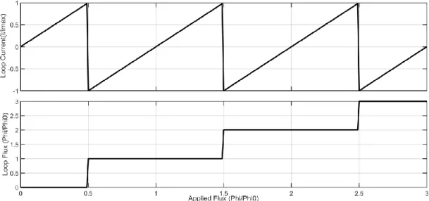
As the value of the external magnetic flux increases, the screening current also increases until the external field reaches 0.5 0, then a 0 field would penetrate in the SQUID loop to decrease the whole energy of the system. Figure 1.12 shows the screening current and the magnetic flux inside the loop as we apply an external magnetic field. The axises of the graphs are normalized for better understanding.
Figure 1.12 : The screening current and penetrated flux of a SQUID loop as we apply external magnetic flux.
In order to read the flux changes better, we apply a bias current to the SQUID loop equal to I=2IC. Because the junctions have same parameters, the current would be equal in both loop branches. Now if there is a magnetic flux that is not an integer coefficient of 0, the currents in the junctions would be:
{𝐼1 = 𝐼 2+ 𝐼𝑖𝑛𝑑 𝐼1 = 𝐼 2− 𝐼𝑖𝑛𝑑 (1.13)
Since the first part of the equation passes the value of the critical current, it would turn normal while the second part would be still superconductor. Therefore, the I-V characteristic of the DC-SQUID would be as in Figure 1.13. Now if we set the flux of the DC-SQUID on the value of (n+0.5) 0 via a compensation coil, the output voltage at the measurement terminals would be maximum. This way, we would have the most voltage to flux ratio and the SQUID would be at the most sensitive state. The output voltage of the DC-SQUID would change by applying external flux as shown in Figure 1.13.
Figure 1.13 : I-V characteristic of DC-SQUID and the output voltage at the terminals [26].
1.2. Outline of the Thesis
The thesis is organized as follows. The general information about the computational power issue and historical background of the Superconductors and superconducting
introduced in Section 2.1 and Section 2.2. The benefits and issues with each technology will be shown in these two sections. The technology we chose for our project and the reasons behind it are explained in this chapter. Then, some of the main cells and designing blocks of complex logics are demonstrated. The digital and analog cells of the RSFQ logics are shown and design principles of these circuits are discussed in Section 2.3. In this chapter, I also show the method of designing RSFQ logics and impedance matching for interfacing circuits. At last the fabrication process and the different layers available for the design of the cells are discussed. In Chapter 3, we will take a look at the arithmetic logic units and the different structures and architectures that they come in. The different architectures for the CMOS process are shown. At the end each of the architectures are described for the RSFQ circuits and the pros and cons of them in RSFQ regime are discussed.
In Chapter 4, the different parts for an arithmetic logic unit are shown. These parts were designed, simulated, fabricated separately and then tested in our system to confirm the function of every circuit. The different parts that are discussed are both from the main circuit of the arithmetic logic unit and the interface registers used for handshaking ALU with lower frequency CMOS logics. All the circuits with their experiment results are demonstrated.
Chapter 5 is the description for the test system. In this chapter our efforts to make a robust system for testing analog and digital circuits in very low temperature and low noise environment is displayed. The test system consists of different parts. The mechanical parts are responsible for cooling down the structure and vacuuming the chamber. The control electric parts are responsible for stabilizing the temperature at stages and control the level of vacuum for safety of system. The measurement parts are in place to supply the needed bias and voltage signals and record data in high and low frequency. All these parts and automation of the test setup is discussed in this chapter.
Finally, Chapter 6 explains the achievements in the thesis and the conclusion of the work. In this chapter two different ALU with different structures are shown and the simulation and test results are discussed as well.
2. SUPERCONDUCTOR CIRCUIT THEORY
After the discovery of superconductors, they were used in many different applications and fields. Most of these applications were using the superconductor as perfect conductor. These applications include power lines [27], fault current limiter switches [28], bolometers [29], narrow band filters [30] and cryotron[ 31]. However, after the Josephson junction discovery, many new applications surfaced. These application included the magnetometer and gradiometer using RF and DC SQUIDS, Josephson voltage standard [32], analog to digital converters quasi one junction SQUID (QOS) and digital logic circuits.
The biggest impact that semiconductor technology had in the last decades is in the field of computing. Josephson junction based logic circuits can contribute to this field dramatically. Although superconductor logic circuits have some drawbacks as in cooling and fabrication, they have advantage over semiconductors in case of speed and power consumption. Semiconductors have been optimized and the fabrication process is advanced for years and they are hitting the limits of the integration and speed limit. The superconductor logic circuits are rather new but they show very reliable function at orders of magnitude lower power consumption and by an order higher speed.
There are different approaches to superconductor circuits. Some include voltage state and flux state logics [33], [34]. Superconductor circuits have been demonstrated with low and high temperature materials. However, the HTS materials are not easily manipulated and the junctions fabricated with these materials would not have desired characteristics. Low temperature materials are easier to work with and there are commercial processes for Nb based superconductors with multiple layers [2].
For every logic design, we need a switch to change the signal path and a memory to store the data bit. In semiconductors the transistor is the switch and the capacitor stores data. In superconductor circuits, the switch is the Josephson junction or SQUID and the memory is the inductance.
Before RSFQ technology and even the invention of Josephson junctions, cryotron superconductor digital circuits were introduced. These circuits used two different superconductor materials with different critical magnetic fields (Hc). As the magnetic field reached the critical value, the material would switch and become resistive. The memory in this material was a simple superconductor loop that could store magnetic flux and therefore current. However this technology was abandoned as the speed of the gates was limited by the (L/R) value and the semiconductors could compete with this speed and had better margins.
In this chapter, we investigate two different Josephson based logics, Rapid Single Flux Quantum (RSFQ) and Adiabatic Quantum Flux Parametron (AQFP). Then we demonstrate some of the cells and basic circuits that we fabricated in these logics. The advantage and disadvantages of these methods will be investigated and finally the fabrication process that we used for the circuits are shown.
2.1. Rapid Single Flux Quantum (RSFQ)
RSFQ was first introduced as alternative superconductor logic by K.K. Likharev and his coworkers. in late 1980s [4], [14]. In this technology, the Josephson junction act as a switch and the data is stored as a magnetic flux in SQUID loops. As mentioned before, RSFQ logic circuits have very low power consumption and therefore are considered to use as an alternative logic in computing centers [35], [36]. The integration capabilities and the high speed of the RSFQ circuits are also dependent on the fabrication process. Various groups are currently working on the processors based on the RSFQ technology [37]–[43].
In RSFQ circuits the data is transferred as a voltage pulse known as single flux quanta (SFQ). Each SFQ pulse has a same energy of one quantum of flux ( 0). The pulses have a width of some Pico-seconds and therefore the circuits can function at hundreds of gigahertzes in theory, such as a toggle flip-flop cell that is reported to work at 770 GHz [44], [45]. Since the storage in the RSFQ circuits are magnetic flux hence current, the bias of the circuits should also be current. The junctions in the RSFQ circuit are current biased up to %90 of their critical value. Figure 2.1 shows the I-V characteristic of the Josephson junction as it is biased.
Figure 2.1 : I-V characteristic of a Josephson junction as it is biased.
Figure 2.1 demonstrates the mechanism of the SFQ pulse generation in RSFQ circuits. As we bias (IB) a junction to near critical current value (IC), if a small current excitation comes to the junction, the current would pass the critical value and voltage would be generated over the junction. The transition that is shown by 2 takes about 1ps time and the junction would go back to the starting point on the path 3. In this transition the phase of the junction changes 2π and the junction would go back to the state that it was in with no memory of the change. In this way, the junction would be similar to a pendulum.
The pulses that are generated in RSFQ circuits are in the order of Pico-seconds and the amplitude depends on the fabrication process. In the standard process which we used for our circuits, the amplitude of the pulses was about 400µV. The fast pulse and the small amplitude make these pulses impossible to observe with our equipment. However, in order to interact with RSFQ circuits, we need to generate SFQ pulses and also read the output of the circuits. Therefore, two circuits are introduced that convert the DC signal (it is called DC because the frequency of changes is really small compared to SFQ pulses) to SFQ pulse and vice versa. The DC/SFQ cell is like a quasi-one junction SQUID (QOS) that detects a threshold and as the current pass that threshold (in our case 1 mA), the circuit generates an SFQ pulse. Figure 2.2 demonstrates the Input and output of the circuit. As seen in the figure, the DC current signal is converted to SFQ pulses and the duration of each pulse is in order of Pico-seconds.
Figure 2.2 : The conversion of DC signal to SFQ pulses with DC/SFQ cell. The counterpart of the DC/SFQ circuit is SFQ/DC circuit that converts the incoming SFQ pulses to DC signal. The SFQ/DC circuit is like a toggle flip-flop that changes the state as it detects an SFQ pulse. On each incoming pulse, if the state is zero, the circuit changes to state one and start oscillating. Since these oscillations are really fast, at the output we only see the average sum of the pulses or the RMS value which is a DC signal. It should be noted that the state of the SFQ/DC is not important and the transitions between each state would determine if we have a data. This is like a transition edge double data rate (DDR) in semiconductor logic. Figure 2.3 shows the difference between single data rate and DDR. Figure 2.4 shows the input pulse and the result for output data [46].
Figure 2.4 : SFQ pulse to DC conversion in a SFQ/DC cell. Note that each pulse causes an state change in the output.
As we discussed before, because of the RSFQ circuits nature, the Josephson junctions are biased with current rather than voltage. Since there in no resistance in the circuits, the static energy consumption of the circuits is zero. However, in large integrated circuits with thousands of junctions, it is not practical to have a bias line for each individual junction at cells. To maintain a correct bias distribution for each junction, a resistance is added at each bias input of a cell. This resistance would enable us to bias the circuits with 2.5mV voltage. The main energy consumption source in RSFQ as mentioned in the introduction is the static power dissipation from these resistances that cause about %99 of the power consumption.
In some other variations of RSFQ circuits such as e-RSFQ (efficient RSFQ) or LRSFQ, these resistances are replaced by a combination of Josephson junction and inductances or just very large inductances respectively. These circuits could consume two orders of magnitude less power but they become much bulkier or compromise the bias margin of a normal RSFQ circuit [47]. In following sections we will discuss more about the RSFQ cells used in our circuits.
2.2. Adiabatic Quantum Flux Parametron (AQFP)
The computation merits of any system are the power consumption and the speed of the system. For many years, the power consumption was not the main issue and the
main focus was on increasing the speed. In recent years due to huge increase in computation needs, power consumption draws attention and is now considered the major metric of the computer design [48]–[50]. As mentioned in chapter 1, Landauer’s law stated that a bit loss in the system causes energy consumption of KBTln2 to compensate the changes in the entropy of the system [51]. This sets the theoretical limit for energy consumption of the logics such as two input gates that have one bit output such as OR gate. However, this limit applies to the logics that have irreversible logic operation including CMOS circuits and RSFQ [12], [13]. Edward Fredkin showed that if we use reversible computers, we can surpass this theoretical limit and have less energy consumption in the system [52], [53]. The Fredkin gate prevent the power consumption resulted from the bit loss by conserving the entropy of the system. The Fredkin gate has 3 inputs and 3 outputs and is reversible since the inputs are derived from outputs. Many different models and physical devices have been investigated for reversible computation [54]–[56].
One of the most efficient computing methods is reversible computing which allows the user to perform the needed calculations without losing any bits. Adiabatic quantum flux parametron (AQFP) is a form of a new superconducting logic that performs reversible computing method system and uses 2 to 3 orders of magnitude less power than former RSFQ circuits by performing reversible computing. In reversible computing because no data bit is lost, its power consumption is smaller than the theoretical Shannon-Neuman-Landauer limit [57]–[59].
Figure 2.5 shows the basics of adiabatic switching. Instead of classical switching which the bit pass through energy barrier and need energy to go back to the state before.
adiabatic regime. Because of the adiabatic nature of these cells the clock frequency of the cells cannot go higher than ~ 5GHz.
Figure 2.6 : The basic operation of an AQFP gate designed by Goto [61]. In Figure 2.6 the Ix is the bias current. There are two superconducting loops that each has a junction. As Ix is coupled to these loops via the mutual inductances, a flux will form in one of the loops depending on the polarization of Iin current. Each flux will determine the state of the output current. Since there is no flux generation and the flux just go from one loop to another on the change of input polarization, the system would work adiabatically and there will be small power dissipation at switching. The bias current is also AC and therefore there is no static power waste.
2.3. RSFQ Cells
After close examination of the available in superconductor logic technologies, we have decided to use RSFQ technology for this project. The factors that we considered include, practicality of design, interface with room temperature systems and CMOS compatibility. RSFQ circuits have been around for 20 years and the basic cells are optimized and have a large bias margin. The fabrication processes are available
commercially for superconductor VLSI. The interface between RSFQ and equipment such as oscilloscope, amplifier and pattern generator is possible due to existence of DC/SFQ and SFQ/DC cells. RSFQ circuits are compatible with CMOS memory after an amplifier stage. Therefore, we decided that we would use RSFQ technology for designing the core of the processor.
There are different circuits and cells available in RSFQ technology. Many of these cells were designed by K. K. Likharev et al. in the first introduction of the technology [4]. Other cells were gradually designed and optimized by various groups throughout the years. The circuits in RSFQ technology can be divided in two main groups. First group are the digital cells that by the pulses, perform digital logic computation. The second set of cells is analog ones. These cells would convert analog signals to digital or perform filtering, wave guides and sensing. The analog cells consist of analog to digital converters such as QOS, CMOS to RSFQ logic converter like DC/SFQ cell and passive transmission lines (PTL) and their driver and receiver that are wave guides for SFQ pulses.
2.3.1. Digital cells
There are various types of digital cells available in RSFQ circuits. The first kind is wiring cells. One of the problems with RSFQ circuits is the fan-out. The fan-out determines that how many inputs a cells output can drive. In RSFQ circuits the fan-out is one. The limited fan-fan-out of the RSFQ circuits causes the need for many cells in the wiring between the gates and the architecture and signal distribution tree to be complicated. For this purpose, many different cells have been introduced. These cells help to overcome the fan-out problem and distribute the signal where ever they are needed without losing data.
Other type digital cells are the logic cells that allow us to perform logic operation on the incoming input data. The logic cells include: AND, OR, XOR and NOT gate. It is noteworthy to mention that all these cells in RSFQ logic regime are clocked. Since RSFQ logic works with pulses rather than voltage level, the clock is needed to control the state of the gate and helps synchronization of the signals by resetting state of the gate to zero. The clock’s importance can be seen well in the Moore diagrams
adder, multiplier and multiplexer. These cells are discussed in detail at coming sections.
2.3.1.1. Wiring cells
One of the most used basic wiring cells in RSFQ technology are Josephson transmission lines (JTL). JTL cell is a transmission line that also acts as a signal router. If the signal gets corrupted due to noise, JTL cell would reform the shape of SFQ signal. Figure 2.7 shows the schematic of a JTL cell.
Figure 2.7 : Schematic of a JTL cell used for RSFQ logic circuits.
In Figure 2.7 we see that the JTL has two Josephson junction, J1 and J2. These two junctions are biased to %90 of their critical currents via the bias line. When a pulse comes from the input port Din, it will pass through the inductances until it reaches the superconductor loop involving the junctions. This loop will not store the SFQ pulse because IcL< 0 and therefore 0 could not be stored inside it. As the outside excitation reaches the loop, the junctions would generate an SFQ pulse and this pulse would travel to the Dout port. The bias resistance is there to insure that at 2.5mV the junctions get the right amount of bias current. The inductances at input and output of the circuit are for the impedance matching. The impedance of the inputs and outputs are set at 2Ω for the circuits designed in standard process. There are many variations
of JTL cell. The schematic of the cells are almost the same but in order to conserve space in big circuits, the layout is altered.
As mentioned before, the fan-out in RSFQ circuits is one. Therefore to distribute a signal pulse to multiple inputs, we have to use a circuit to split a signal to more signals. This circuit is known as splitter. The splitter could multiply an incoming signal to two or three pulses.
Figure 2.8 shows the schematic of a splitter cell used in RSFQ circuits. The first part of the circuit until the two way is a buffer stage like half a JTL cell. This stage assures that the SFQ pulse is in right shape and the impedance of the input is matched with other circuits. Since there is no resistance in RSFQ circuits, the voltage splits according to the inductances at two ways. The inductances for both branches are the same in the splitter, therefore the signal would be halved and enter each branch. The critical current value for J2 and J3 junctions are small, therefore, they would response to smaller excitation and create SFQ pulse. As the inductances and the junction values are similar in the splitter, the output pulses would exit the circuit via port B and C at the same time.
Figure 2.8 : Schematic of a RSFQ splitter cell.
The other wiring cell that we used in this work is the merger. Merger cells act as the opposite of splitter cell. When two SFQ pulses come to the merger at the same time,
buffer line. Like splitter this JTL at inputs would guaranty the shape of the SFQ pulse and impedance match to other circuits. As an SFQ pulse comes from one of the inputs, J3 or J4 junctions would pass portion of that pulse through and that is enough to excite J5 to generate a pulse. J3 and J4 junctions also prevent the pulse from reflecting and going back to the inputs.
Figure 2.9 : Merger circuit schematic for RSFQ process.
When two SFQ pulses simultaneously or with very small time difference come from both the inputs, after passing through J3 and J4 junctions would not be strong enough to excite J5 to generate two SFQ pulses and instead it only generates one pulse in the output.
2.3.1.2. Logic cells
Logic cells are the basic blocks for the digital circuits and digital computing. In this section we will discuss the four main gates that exist in RSFQ technology. These gates include AND, OR, XOR and NOT. As mentioned before, because of the RSFQ logic’s pulsed nature, all the gates in this technology are clocked.
The first gate that we discus here is the AND gate. The AND logic is true when all of the inputs are present. Figure 2.10 is the Moore diagram of a Josephson AND gate as presented in [62], [63].
Figure 2.10 : Moore diagram of the Josephson AND gate [62].
The cell’s state is not clear as we apply bias to activate it. Therefore we should apply a clock signal at first to reset the cell to state zero. After that depending on the incoming input, the circuit would switch to state 1 or 2. At this point, if the clock signal comes the cell would go back to state zero and would be reset. However, when the other input comes at the states 1 or 2, the device would go to state 3 and by incoming clock signal we would have an SFQ pulse at the output.
The main difference that we see here between RSFQ AND logic and CMOS AND logic is the lack of clock signal in the CMOS AND. The pulse nature of the RSFQ logic make us to store the coming signal inside the logic and make the operation with the clock signal to prevent data loss.
The function of the AND cell can better be understood in Figure 2.11. As it is shown in the schematic of the cell, the first stages after the input are similar to JTL. This stage would ensure that the signal is corrected and has a right timing. As the inputs
![Figure 1.2 : The critical temperature of different superconductors versus the year of their find [20]](https://thumb-eu.123doks.com/thumbv2/9libnet/3754660.28203/32.892.116.726.247.766/figure-critical-temperature-different-superconductors-versus-year.webp)
![Figure 1.6 : Josephson current versus the magnetic field for two parallel junctions [24]](https://thumb-eu.123doks.com/thumbv2/9libnet/3754660.28203/35.892.176.782.482.891/figure-josephson-current-versus-magnetic-field-parallel-junctions.webp)
![Figure 1.13 : I-V characteristic of DC-SQUID and the output voltage at the terminals [26]](https://thumb-eu.123doks.com/thumbv2/9libnet/3754660.28203/42.892.100.730.506.884/figure-i-characteristic-dc-squid-output-voltage-terminals.webp)
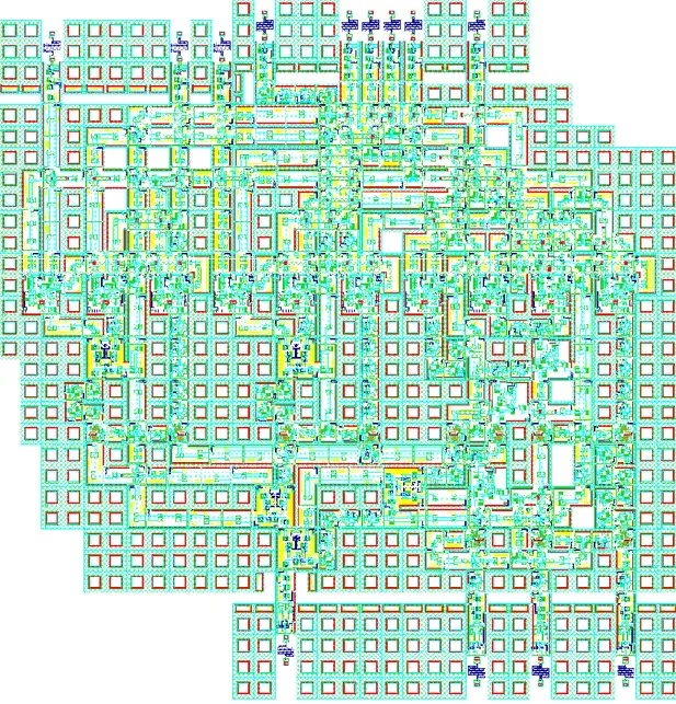
![Figure 3.3 : FLUX-1R chip layout designed w,ith 63107 Josephson junction. The power dissipation of the chip is about 10mW [71]](https://thumb-eu.123doks.com/thumbv2/9libnet/3754660.28203/75.892.166.810.115.771/figure-flux-layout-designed-josephson-junction-power-dissipation.webp)
![Figure 3.5 : The block diagram for 4-bit ALU based on HA and switches [72]](https://thumb-eu.123doks.com/thumbv2/9libnet/3754660.28203/77.892.157.807.253.540/figure-block-diagram-bit-alu-based-ha-switches.webp)
![Figure 3.7 : Block diagram of the processor architecture in the CORE e design [74]](https://thumb-eu.123doks.com/thumbv2/9libnet/3754660.28203/79.892.172.804.156.614/figure-block-diagram-processor-architecture-core-e-design.webp)