IEEE Africon 2002 535
A BROADBAND MICROWAVE AMPLIFIER DESIGN BY MEANS OF IMMllTANCE
BASED DATA MODELLING TOOL
A &Impt)
H Pinarbqi('1M $engiiP' BS
Yarman~ll
"'Isik University, "'Kadir Has University, Istanbul, TurkeyABSTRACT
In this paper a practical broadband microwave amplifier design algorithm is introduced utilizing the immittance data-modelling tool. In the course of design, f i i , the optimum input and output terminations for the active device are produced employing t h e real frequency technique. Then, these terminations are modelled utilizing the new immittance-modelling tool t o synthesize the front-end and back-end matching networks. An example is included to exhibit the implementation of the proposed design algorithm to construct a single stage BJT amplifier over a wide frequency band. It is expected that the proposed design algorithm will find applications to realize widehand microwave amplifiers put on MMIC for mobile communication.
1. INTRODUCTION
One of the fundamental problems in the design and development of communication systems is to match a given device to the system via coupling circuits so as to achieve optimum performance over the broadest possibie frequency band. This problem inherently involves the design of an equalizer network to match the given complex impedances, and usually referred as impedance matching or equalization.
Recently introduced immittance data modeling tool can be employed successfully to design microwave amplifiers [I]. As indicated in [I], design of microwave amplifier, falls in problems of Type 11 category. When a broadband microwave amplifier is designed, optimum termination immitances for the active device can be generated point by point employing the Carlin's Real Frequency Line Segment Technique [2-51. Then, the data for the terminations are modelled by means of the immitance modeling tool. Eventaully, Positive Real (PR) immitances are synthesized to yield the front-end and the back-end matching networks which completes the design.
Therefore, in this presentation, first the immitance based modeling tool is summarized. In section 111, Generalized Real Frequency Technique (GRFT) is outlined. The complete design algorithm is given in Section IV. Finally, utilization of the design algorithm is exhibited with an example.
The process described in this paper can easily be extended to design microwave amplifiers with mixed lumped and distributed elements [ 6 ] . It is expected that the design technique introduced in this paper will find application to
realize microwave amplifiers on MMIC for mobile communication.
2. THE IMMI'ITANCE BASED DATA
MODELLING TOOL [l]
Any positive real rational immittance function F(s) can be written in terms of its minimum and the Foster parts;
F ( s ) = F, ( s ) + F/ ( s ) (1) where s = U
+
j o is the complex domain variable,F,,,(s) is the minimum part which is free of j w poles, and
F/(s)
is the Foster part which includes only j opoles. On the real frequency axis j w
,
one has F ( j o ) = R ( o )+
j X ( o ) F A ~ O J ) = ~ , ( w i + j ~ , ( o ) (2) F j ( j o ) = j x , ( o ) It is clear that (3 ) R(o) =R,
(4
X ( o ) =x,"
(0) +x,
(0)Since F,,,(s) is a positive real minimum, which contains no poles on the j o axis, its imaginary part X , ( w ) is related to the real part R,(o) by the Hilbert transformation relation;
X , " ( W ) = H { R ( w ) } (4) where
operation.
In the immittance based modelling technique, the crux of the matter is to decompose the given data into its minimum part and Foster part. Hence, the modelling process is carried out within two major steps: model for the minimum part and the Foster part.
To model the minimum part, it is sufficient to match an analytic form R ( o z ) for the real part data. Then the complete minimum function F(s) can easily be generated from R(-s2) by means of Gewertz procedure [4].
IEEE Africon 2002
The real part forms are classified based on the selection of the transmission zeros of the matching networks. Let R ( 0 2 ) =
*,
in this case regarding the zeros ofD(w )
N(o') ,the real part forms are described as follows: For modelling Form-A N ( o ) = 02'
For modelling Form-B For modelling Form-C
N ( o ) = oZkfi(cu2 -oZp)'
p=l
These choices will be picked in accordance with the given data for
R(w)
.In order to extract the Foster part from the original measured data, one has to generate X , ( w ) using the Hilbert Transformation relation [3]. Eventually, realisable analytical forms for the minimum immittance function and the Foster function are obtained by means of an appropriate curve fitting or interpolation algorithms and they are synthesized to yield the desired model under consideration.3. GENERALIZED LINE SEGMENT
TECHNIQUE FOR MATCHING A
COMPLEX LOAD TO A RESISTIVE
GENERATOR
Consider the single matching circuit arrangement shown in Figure 1.
I
1I
z,,,
Z , = R,+
j X ,I
Figure 1: Single matching problem
Let the load impedance ZL and the equalizer back impedance 2, be written in terms of their real and imaginary parts on the real frequency axis as
Basic idea is the use of
a
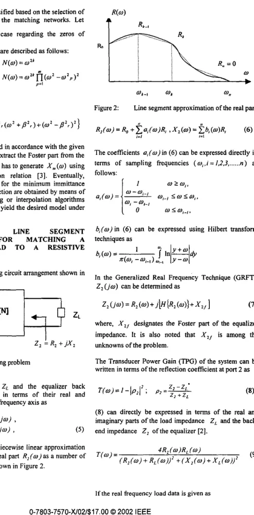
piecewise linear approximation to represent the unknown real part R, (CO) as a number ofstraight-line segments as shown in Figure 2.
536
!
0-7803-7570-X/02/$17.00
0
2002IEEE
Ok-I ok 0,
Line segment approximation of the real part Figure 2:
The coefficients a I ( w ) in (6) can be expressed directly in terms of sampling frequencies ( o,,i=1.2.3
,...
n ) as follows:b , ( w ) in ( 6 ) can be expressed using Hilbert transform techniques as
b, (0) =
In the Generalized Real Frequency Technique (GRFT), 2, (jo) can be determined as
where, X,, designates the Foster part of the equalizer impedance. It is also noted that
X,,
is among the unknowns of the problem.The Transducer Power Gain (TPG) of the system can be written in terms of the reflection coefficient at port 2 as
(8) can directly be expressed in terms of the real and imaginary parts of the load impedance ZL and the back- end impedance
Z,
of the equalizer [2].IEEE Africon 2002 537
Z,(jw)= R L ( j o ) + j X L ( j c a ) , then the matching problem becomes essentially to that of finding Z,(jo)point by point such that T ( o ) is maximized over the band of operation.
Once Z,(jw)= R , ( o ) + j X , ( o ) i s determined point by point employing the Generalized Real Frequency Technique, it is modelled as a positive real function by means of the "immittance based data modelling tool[I]". In the following section, we will introduce the new microwave amplifier design technique via the immitance modelling tool.
3.1 Extension of Immittance Based Data Modelling Tool to the Design of Amplifiers
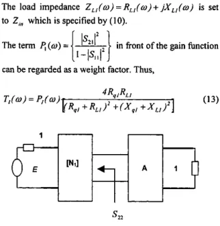
Let us consider the single stage amplifier configuration shown in Figure 3 where the active two-port device is denoted by [A]. The lossless two-ports N I and N, designate the front-end and back-end matching networks respectively. A single stage microwave amplifier can conceptually be constructed within two steps by using the Real Frequency Technique. In the first step, the optimum immitance data Z,, for the front-end matching network is generated point by point over the band of operation. In this step, we presume that the output port of the active is closed with unit termination (i.e. 50 ohms) (Figure 4). Hence, the input impedance of the transistor is given by
(10)
I + SI,
z,,
=-
/-si,
and it is considered as the termination of the input matching network.
m
Figure 3:and output
In this case, we face a single matching problem. Thus, employing the GRFT, optimum impedance data Z,! for the front-end matching network is generated. The gain of the system shown in Figure 4, is given by
Single stage amplifier equalized at both input
In ( 1 I), the driving point input impedance of the front-end equalizer is
The load impedance Z L , ( o ) = RLI(o)+ jX,,(o) is set to
Z,,,
which is specified by (IO).The term
4
(0) = [ I-
:j:r]
in front of the gain function can be regarded as a weight factor. Thus,s,,
Figure 4: Single stage amplifier equalized at the input In this step, the negative slope of the gain is compensated by optimizing T, to a flat gain level To,
.
In the second step of the conceptual design, the back-end matching network will be generated as set of data. In this case, the gain T , ( w ) , which is subject to optimization, is expressed in terms of the driving point impedance Z , , of the output- matching network N,
In (14), the term S22 is the reflection coefficient of the
active device seen at the output when the front-end matching network is present. Hence,
In (15),
S,,
is the input reflection coefficient of the front- end equalizer and it is given byFurthermore,
(17)
I
+
S nI - s 2 z
Z,, =
-
= R,, + jX,,the gain of the overall system is given by
Finally, optimization of T2(w) to a flat gain level To, yields the Thevenin's impedance Z,, as set of points. In the first step, it would b e wise to select To, as the minimum value of
-
'sz"
over the operation band. Similarly in the second step, one can choose To, as theI-IS,,I2
the specified frequencies
In the course of the optimizations
Z,,(jw) = R , , ( w ) +
jX,,(o)
are computed point by point as described in the Generalized Real Frequency Technique (GRFT). To improve the optimization, the imaginary partsX ,
can be computed asX ,
= H { R ,)+
X,,
,
i = I,?. whereX,
designates the Foster parts of driving point impedance Z ,.
The above-mentioned process is summarized in the following algorithm.
4.
Z,, ( i w ) = R,, (0) +
Jx,,
(a) andTHE
ALGORITHM. DESIGN OF A SINGLE STAGE MICROWAVE AMPLIFIERPart I: Design of front-end equalizer Inputs:
S,,,S,,,S,,,S2, : The Scattering parameters of the active element over the prescribed frequency band.
Computation steps:
Step I: Construct the weight function
Here, the terms R,and
X,
refer to the real and imaginary parts of the input impedance of the transistor when its output is loaded by I-ohm resistor, which is given by the equationZ, =
5
= R,+ jX,
.
The terms R,, and X , , refer1-sll
to the real and imaginary parts of the output impedance of
the front-end matching circuit respectively.
Step 111: Optimize the gain function T,(ru) to obtain a flat
gain level of min
{
-
I ! & f ]
And determine the break points for Z,, as described in the GRTF.
Step Tv: Having obtained the data for Z,,
,
generate the analytic form for it using immittance based modelling tool and synthesize it.Step V By using this analytic form of the impedance
Z,,
,
compute the front-end and the back-end matching networks reflection coefficients as follows.Using (b) calculate the load impedance I + S ,
(C)
z,,
=-
I-s,
= R,,+
jX,,Save the terms T l ( w ) . Z L , . S , that have just been computed . The first part of the algorithm is completed. Part 11: Design of back-end equalizer
Inputs:
S,,.S,,.S,,,S,,
: The Scattering parameters of the active element over the prescribed frequency band.S, and Z,, (calculated at the end of the first step) Computation steps:
Step I: Construct the weight function T , ( w )
P J w ) =
-
Step 11: Construct the gain function
I-IS,S
Step 11: Construct the gain function
0-7803-7570-X/02/$17.00
02002
IEEEIEEE Africon 2002 539
Transducer power gain TI is compensated to a flat gain level To, =17dB. In this design, there was no need to employ foster part for Z,,,. Hence, as the result of optimization R,, is computed
R., = /1.036168e-i 7.956833e-2 1.189832e-1 T , ( ~ ) = p z ( ~ ) l 4Rv,RL2
The terms R, and
X,
refer to the real and imaginary(R,, +R,,)’
+(x,,
+X,,J~I
7 .
-
parts of the output impedance of the transistor when its
input is loaded by the front-end matching circuit, which is l,943650e-1 3,186138e- I given by the equation
Z, =
3
= R,+
j X ,.
The terms R,, andX,,
refer to the real and imaginary parts of the output impedance Ofthe back-end matching circuit respectively.
Step Ill: Optimize the gain function TI(@) to obtain a flat
gain level of win[
-A}
And determine Z,,point by point to optimize
T, employing GRFT.
X,,
= [8.627670e - 3 3.909525e-
2 9. I18513e - 2 Step IV: Having obtained the data for Z,, generate theanalytic form for it using immittance based modelling tool and synthesize it.
Part 11: In this part the back-end matching network is constructed when the front-end is present. Similarly, supplying the initial guess values for the resistive excursions &,, T, is optimised to a flat gain level ToZ=15dB. As the result of optimisation Rq2 is found as
R,, = [7.633953e - I 1.131313 9.398499e- I 7.549760e
-
I 7.55651 le - I 7.707590e-
I ] Evaluation ofX,
(0) at the break frequencies yieldsI-s,
I-PIII l - 1 ~ 2 2 1
1.265858e- I 1.727060e- I -2.587056e-I]
A‘,, = [-7.650150e - 2
-
2.538549e - I-
5.712840e-
1 -6.412332e-1 -7.Ol2788e-1 -1.03125OJNow, let us introduce an example to design a single stage
amplifier. By using the immittance based data modelling tool, the
minimum reactance functions can be calculated analytically and this leads to the synthesis of the equalizer
5. EXAMPLE
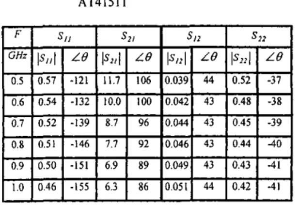
circuits. For both front-end and back-end matching In this example, we wish to design a microwave amplifier networks, modelling form A is selected for R ( 0 2 ) employing the immittance-based data-modelling tool. For The program code was run and at the end the minimum this purpose commerciab’ available transistor HP- reactance functions for the input and the output equalizers AT4151 1 was selected and its biasing conditions are were found to be
V,, = 8V.1, = IOmA.Z, = 5 0 0 Bandwidth = 500 MHz. (500MHz-IGHz) 2 . 0 8 7 ~ ’ ~ 5 . j 8 9 S ’ + 4 5 9 S s + 1 . 3 6 3 10955s‘ t 29342’ s 3 4 0 3 I P ~ 3 3 6 9 S S + 19.400 ~ , , , , - p w , ,
-
4.4/ls’+2.599s2 +4.502s+0.668 10.069s‘ +5.934s3+
1 5 . 8 5 8 ~ ~ t 4 . 8 1 4 ~ +4.261 Table 1 : Typical Scattering Parameters for HP- , .,Z,,, =AT41511
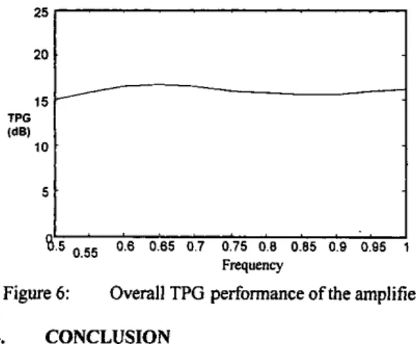
The final amplifier configuration and overall performance curve are given in Figure 5 and Figure 6 respectively.
~
f..,~
iTTl
0.6684 0.438 0.204
0.062
Figure 5 : Designed amplifier configuration Part I: In this part of the algorithm we selected 6 break
frequencies w, =SOOMhaz, w 2 =600Mhz, w, =700 Mhz, o,=BOOMhz, #,=900Mhz and @,=I GHz. The
IEEE Africon 2002
5 1
Frequency
Figure 6: Overall TPG performance of the amplifier
6. CONCLUSION
In this paper, the immitance data-modelling tool is applied to design single stage microwave amplifiers. On the other hand, optimum immitance terminations for the active device are generated employing the Generalized Real Frequency Technique. An algorithm is presented to ease the understanding of the design process introduced in this paper. Implementation of the algorithm has been exhibited by means of an example. It can readily be seen that the single stage microwave amplifier design algorithm involves only simple linear arithmetic computations during optimization routine, while processing numerically defined load impedances of any complexity. The gain function is quadratic in the unknowns, and hence the problem reduces to that of a quadratic optimisation. The design algorithm presented here, can easily be extended to construct microwave amplifiers with mixed, lumped and distributed elements, employing realizable, two variable, driving point network functions [a].
7.
REFERENCES
[l] Yarman, B.S, Aksen, A., Kilinq, A.: “An Immittance Based Tool for Modelling Passive One-Port Devices by Means of Darlington Equivalents” A.E.U 55 No.6, December 2001, pp.443-451
121 Carlin. H.J.: “A New ADDroach to Gain- Bandwidth Problems” IEEE Trans. ‘cas, Vo1.23, April
1977, pp.170-175
[3] Yarman, B.S., Carlin, H.J.: “A Simplified Real Frequency Technique Applied to Broadband Multistage Microwave Amplifiers” IEEE Tramon MTT 30 1983, pp. 15-28
[4] Yarman, B.S.: “Cok Katli Mihodalga Kuvvetlendiricileri Tasarim YBntemleri” TUBiTAK Project Report, May 1985
[5] Yarman, B.S.: “Real Frequency Broadband Matching Via Linear Programming” RCA Research Center Princeton NJ,Novemher 1982
0-7803-7570-X/02/$17.00
0
2002 IEEE540
[6] Aksen, A., Yarman, B.S.: “A Real Frequency Approach to Describe Lossless Two-Ports Formed With Mixed Lumped and Distributed Elements” A.E.U 55 N0.6,
December 2001, pp.389-396
Ali IOIinc received B.Sc. and M.Sc. degrees in electronics engineering 6om Uludag University, Bursa, Turkey in 1986 and 1989 respectively. He completed his Ph.D in the area of impedance modeling at Istanbul University, Turkey in 1995. Until1 1988 he was a lecturer at Istanbul University. Then he joined Nortel Networks-Netq, Turkey. He is working at
Ivik University since 2001. [email protected]
Haci Pinarbafi received BSc. and M.Sc. degrees in electronics engineering 60m Istanbul University and Bogazici University, Istanbul, Turkey in 1998 and 2002 respectively. He was a teaching assistant at department of mathematics at Yeditepe University, Istanbul, 6 o m 1998 to 2000. He is a research assistant since 2000 and a Ph.D student at ISik University, Istanbul, Turkey.
hD0isikun.edu.i
Metin SengUl received BSc. and M.Sc. degrees in electronics engineering 6om
Istanbul Universitv. Turkev in 1996 and _ . 1999 respectively. He worked as a
’ technician at Istanbul University 6om
1990 to 1997. He is a teaching assistant at Kadir Has University, Istanbul, Turkey since 2000 and he is a Ph.D student at I$ik University, Istanbul, Turkey.
B. Siddik Yarman received the B.Sc. degree in electrical engineering 6om the Technical University of Istanbul (I.T.U), Istanhul,Turkey, in 1974 and the M.E.E.E 60m Stevens Institute of Technology (S.1.T) in NJ, in 1977, and the W.D. degree h m Comell University, Ithaca, NY, in 1982. He was a member of the technical staff with David Samoff Research Center, NJ, 60m 1982 to 1984 and associate professor with Anadolu University and Middle East Technical University in 1985-1986. From 1987 to 1989 he was a visiting professor at Ruhr University, Bochum, Germany as an Alexander von Humboldt Fellow. He was a full professor at Istanbul University until1 1996. Since 1996 he is the president of I$ik University, Istanhul, Turkey. Dr. B.S. Yarman holds four US. patents, recipient of research and technology award of the National Research Council of Turkey; selected as the international man of year in Science and Technology by Cambridge Biography Center of U.K. in 1998. He is the member Academy of Science of New York, senion member of IEEE.
yarman0isikun.edu.tr