NANOSTRUCTURED MATERIALS AND
DEVICES FOR SENSING AND ENERGY
HARVESTING APPLICATIONS
A DISSERTATION SUBMITTED TO
THE GRADUATE SCHOOL OF ENGINEERING AND SCIENCE OF BILKENT UNIVERSITY
IN PARTIAL FULFILLMENT OF THE REQUIREMENTS FOR THE DEGREE OF
DOCTOR OF PHILOSOPHY IN
MATERIALS SCIENCE AND NANOTECHNOLOGY PROGRAM
By
Mehmet Kanık
August, 2015
I certify that I have read this thesis and that in my opinion it is fully adequate, in scope and in quality, as a thesis of the degree of Doctor of Philosophy.
………. Prof. Dr. Mehmet Bayındır (Advisor)
I certify that I have read this thesis and that in my opinion it is fully adequate, in scope and in quality, as a thesis of the degree of Doctor of Philosophy.
………. Prof. Dr. Adnan Akay
I certify that I have read this thesis and that in my opinion it is fully adequate, in scope and in quality, as a thesis of the degree of Doctor of Philosophy.
………. Prof. Dr. Salim Çıracı
I certify that I have read this thesis and that in my opinion it is fully adequate, in scope and in quality, as a thesis of the degree of Doctor of Philosophy.
………. Prof. Dr. Haluk Külah
I certify that I have read this thesis and that in my opinion it is fully adequate, in scope and in quality, as a thesis of the degree of Doctor of Philosophy.
………. Prof. Dr. Aydın Doğan
Approved for the Graduate School of Engineering and Science:
………. Prof. Dr. Levent Onural Director of the Graduate School
ABSTRACT
NANOSTRUCTURED MATERIALS AND DEVICES FOR
SENSING AND ENERGY HARVESTING APPLICATIONS
Mehmet Kanık
Ph.D. in Materials Science and Nanotechnology Supervisor: Prof. Dr. Mehmet Bayındır
August, 2015
A closer look into the fundamental challenges of the modern world reveals that the increasing demand for energy threatens the evolution of science and technology. Energy-efficiency is thus a fundamental issue in engineering nano-devices. An important path to achieve high efficiency is to convert the mechanical energy into electrical energy using piezoelectric and triboelectric energy harvesting circuitries, hence enabling self-powered systems at nanoscale. The utilization of novel piezoelectric and triboelectric energy harvesting materials introduces the opportunity of manufacturing flexible, wearable and stretchable self-powered devices.
In this thesis, we introduced a new fabrication technique, new strategies and practical approaches for developing high performance triboelectric and piezoelectric materials and devices for flexible electronics, artificial skin and energy harvesting applications.
The first part of the thesis focuses on the development of piezoelectric nanoribbons. Poly (vinylidene fluoride) and its copolymer Poly (vinylidene fluoride)-co-tri (fluoroethylene) were used to fabricate spontaneously high piezoelectric nanoribbons. We measured the record-high piezoelectric charge coefficient from our ribbons, because the high stress and high temperature used in the fabrication can enhance their properties. In addition, proof of principle devices for energy harvesting and sensing were fabricated using nanoribbons. The achievements in this part of the thesis can be listed as: i) We obtained extraordinary high aspect ratio, globally oriented, polymer encapsulated, and high piezoelectric microribbon and nanoribbon arrays. ii) Due to
any electrical poling. iii) We developed a new technique for characterizing and analyzing multiferroic characteristics of nano-objects, which consist of parallel evaluation of instrumental, numerical and analytical data. iv) To our knowledge, we achieved the highest piezoelectric charge coefficient from our ribbons in the literature. v) We enhanced stability of the piezoelectric ribbons by increasing the Curie temperature above its melting point due to processing conditions. vi) We observed and explained a new phase transformation mechanism in polymer piezoelectric ribbons. vii) The state-of-the-art ab initio calculations, which explain the phase transformation mechanism of molecules during the fiber drawing with the effect of shear, tensile forces and temperature, were included in detail.
The second part is about developing high energy output triboelectric generators. A high performance multi-layered triboelectric generator was developed using chalcogenide nanostructures. This part of the thesis details the following achievements: i) We demonstrated that not only polymer, but also semiconductor chalcogenide materials can be used in triboelectric applications, for the first time. ii) For the first time, we proposed and demonstrated that the fluorination of nanostructured surfaces increases triboelectric performance significantly. iii) We introduced a multi-layered triboelectric generator which is very promising for real applications such as acoustic wave and vibration detection, and energy harvesting with very high power output (0.51 Watt) in comparison with the literature. iv) We used a 3D printing technique to produce our device, which is low-cost and appropriate for rapid prototyping and mass production. v) We explained the device theory for the triboelectric nanogenerator, which aligned well with our experimental results.
Keywords: Iterative size reduction technique, energy harvesting, triboelectricity,
ÖZET
ENERJİ ÜRETİMİ VE SENSÖR UYGULAMALARI İÇİN NANO
YAPILI MALZEMELER VE NANO AYGITLAR
Mehmet Kanık
Malzeme Bilimi ve Nanoteknoloji, Doktora Tez Yöneticisi: Prof. Dr. Mehmet Bayındır
Ağustos, 2015
Modern dünyanın temel sorunlarına yakından bir bakış attığımızda, artan enerji ihtiyacının bilim ve teknolojinin gelişimini tehdit ettiğini görmekteyiz. Süregelen problemlerin, düşük enerji gerektiren cihazlar üreterek ve kayıp enerjiyi geri dönüştürerek çözülmesi hedeflenmektedir. Düşük enerji sarf eden cihazlar ile piezoelektrik enerji üretim devreleri kullanarak mekanik enerjinin elektrik enerjisine dönüştürülmesini sağlayarak kendi enerjisini üretebilen sistemlerin entegre edilmesi mükemmel bir çözüm olarak görülmektedir. Daha da ötesi, yüksek performanslı triboelektrik ve piezoelektrik malzemelerin kullanımına ihtiyaç duyulduğu organik piezoelektrik ya da yüksek performanslı triboelektrik nano-jeneratörlerin üretilmesi ile esneyebilir, giyilebilir ve sünebilir, kendi enerjisini kendi üreten cihazların geliştirilmesi fırsatını ortaya koymaktadır.
Bu tezde yeni bir üretim tekniği, esnek elektronik, yapay deri ve enerji üretimi uygulamaları için, yüksek performanslı triboelektrik ve piezoelektrik malzemelerin geliştirilmesinde yeni stratejiler, pratik yaklaşımlar anlatılmaktadır. Bu tez iki ana kısımdan oluşmaktadır. Birinci kısım piezoelektrik nano şeritlerin üretimini içermektedir. Poly (vinylidene fluoride) ve onun kopolimeri olan Poly (vinylidene fluoride)-co-tri (fluoroethylene) malzemeleri kendinden yüksek piezoelektrik özelliği gösteren nano şeritlerin üretiminde kullanılmıştır. Ardışık fiber çekme yönteminde kullanılan yüksek sıcaklık ve stres gibi parametrelerin etkisiyle, ürettiğimiz şeritlerden rekor yükseklikte piezoelektrik yük katsayısı ölçtük. Ayrıca, nano şeritler kullanılarak enerji üretimi ve sensör amaçlı cihazlar geliştirildi. Bu tezin birinci kısmında elde edilen kazanımlar şöyle sıralanabilir: i) Sıra dışı uzunluk oranlarına sahip, aynı
gösteren mikro ve nano şeritler elde ettik. ii) Termal fiber çekme parametreleri (kayma gerilmesi ve sıcaklık) sebebiyle, üretilen mikro ve nano şeritlerde, elektriksel polarizasyon işlemi gerektirmeksizin, yüksek oranda polar faz elde edilmiştir. iii) Nano objelerin çoklu ferroik karakteristiklerini incelemek için, enstrümantal, sayısal çözümleme ve analitik tekniklerin paralel olarak kullanıldığı, yeni bir yöntem geliştirdik. iv) Bilgimiz dâhilinde, literatürde bildirilen en yüksek piezoelektrik katsayı bizim nano şeritlerimizden ölçülmüştür. v) Üretim parametreleri sayesinde, Curie sıcaklığını erime sıcaklıklarının üzerine çıkararak piezoelektrik şeritlerin kararlılığını arttırdık. vi) Polimer piezoelektrik şeritlerde yeni bir faz dönüşüm mekanizması gözlemledik ve bu mekanizmayı açıkladık. vii) Modern ab initio hesaplamaları kullanılarak, kayma gerilimi, çekme gerilimi ve sıcaklık gibi fiber çekme parametrelerinin etkisi ile moleküllerde oluşan faz dönüşümü detaylı olarak açıklandı.
İkinci kısım ise, yüksek enerji üretimine sahip triboelektrik jeneratörlerin geliştirilmesini hakkındadır. Kalkojen nano yapılar kullanılarak yüksek performanslı, çok katmanlı triboelektrik nano jeneratör geliştirildi. Tezin bu kısmı aşağıda listelenmiş yönleri ile tanımlanabilir: i) İlk kez, sadece polimerlerin değil, yarı iletken kalkojenlerinde triboelektrik jeneratör uygulamalarında kullanılabileceğini gösterdik. ii) Nano yapılı yüzeylerin flor ile kaplanması sonucu triboelektrik özelliklerinin önemli miktarda artacağını ilk kez önerdik ve gösterdik. iii) Akustik dalgaların ve titreşimin algılanması, literatürde ki eş denekleri ile karşılaştırıldığında, çok yüksek çıkış gücüne (0.51 Watt) sahip enerji üreteci gibi gerçek uygulamalarda kullanılabilecek, çok katmanlı triboelektrik bir triboelektrik jeneratör geliştirdik. iv) Bahsi geçen cihaz, düşük maliyetli, hızlı üretim ve seri üretime uygun, 3D yazdırma tekniği ile üretildi. v) Triboelektrik nano jeneratörlerin teorisini açıkladık ve deneysel sonuçlarımız ile analitik sonuçlarımızın mükemmel şekilde örtüştüğünü gösterdik.
Anahtar kelimeler: Ardışık boyut küçültme tekniği, enerji üretimi, triboelektrik,
Acknowledgement
I would like to thank my advisor, Prof. Dr. Mehmet Bayındır, for providing a fruitful and rich research environment during my PhD, sharing personal and academic experiences with me. He was always helpful for solving the scientific and technical problems along my PhD. Especially in last 3 years of my PhD, he allowed me to do research freely, so I had chance to learn new subjects and improve my skills.
I would like to thank also to my PhD thesis committee, especially to Prof. Dr. Adnan Akay and Prof. Dr. Salim Çıracı for encouraging me to do my research in depth.
In particular, I give my special thanks to Bayındır Group Laboratory coordinator, Murat Dere for being a good friend and helping me all the time. Besides I want to thank our project coordinator Neşe Özgür for her always smiling face and her helps.
I particularly thank to my team mates and friends, M. Girayhan Say, Dr. Ozan Aktaş, Bihter Dağlar, Alp Emre Acar, Umar Musa Gishiwa, Ahmet Faruk Yavuz, Muhammad Yunusa for sleepless nights we spent in UNAM and their cheerful conversations. I especially thank Ozan for the software that he developed for our group. I should also mention my gratitude to all present and past group members and all other people who helped me in during my research. I also like to thank Asst. Prof. Dr. Engin Durgun and Dr. H. Sener Sen for ab initio calculations, and I like to thank Merve Marcali and Asst. Prof. Dr. Caglar Elbuken for microfluidics experiments.
I want to thank my good friend Sencer Ayas for encouraging conservations, commenting on my researches. I like to thank Asst. Prof. Dr. Tarık Baytekin, for enjoyable scientific conversations. I also specially thank Asst. Prof. Dr. Gökan Bakan, Dr. Kemal Çelebi, Mustafa Ürel and Hasan Güner for being good friends and proof reading my papers.
My greatest gratitude and thanks goes to my mother Muteber Kaya, who dedicated her life, ignored her own needs and demands for raising her 3 children by herself. And of course, the woman who is my fellow in this life, Dr. Zeynep Hazar, deserves also my greatest gratitude. I appreciate her understanding and encouraging conversations. The research leading to this thesis has received funding from the European Research Council under the European Union's Seventh Framework Programme
Contents
ABSTRACT ... iv
ÖZET ... vi
Acknowledgement ... viii
Contents ... x
List of Figures ... xiv
List of Tables ... xxviii
Chapter 1 Introduction ... 1
1.1. Piezoelectricity ... 7
1.1.1. Piezoelectric Effect ... 7
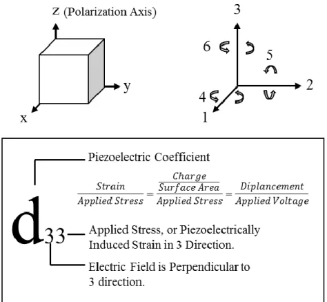
1.1.2. Piezoelectric Constants and Linear Piezoelectric Equations ... 9
1.2. Triboelectricity and Source of the Static Charges ... 16
1.2.1. Triboelectricafication ... 17
1.3. Thesis Outline ... 22
Chapter 2 Iterative Thermal Size Reduction Technique for Multi-material Nanostructure Fabrication ... 23
2.1. Top-Down and Bottom-Up Fabrication ... 24
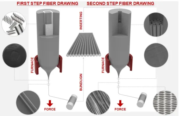
2.2. Iterative Fiber Drawing Technique ... 25
2.2.1. Possible Applications of Nanofibers ... 29
2.3. Kilometer-long Nanotubes and Nano-shells ... 31
2.3.1. Fabrication Process ... 34
2.3.2. Morphologic Characterization ... 40
Chapter 3 Spontaneous High Piezoelectricity in Poly (vinylidene fluoride)
Nanoribbons Produced by Iterative Thermal Size Reduction Technique ... 46
3.1. Introduction ... 47
3.1.1. Piezoelectric Properties and Phases of Poly (vinylidene fluoride) ... 47
3.1.2. Fabrication Methods Triggering to Polar Phase Transition ... 49
3.2. Fabrication of Kilometer-long Piezoelectric Nanoribbons ... 51
3.2.1. Temperature and Shear Induced Phase Transformation ... 52
3.2.2. Preform Fabrication ... 53
3.2.3. Iterative Fiber Drawing ... 54
3.2.4. Morphological Characterization ... 55
3.2.5. Molecular Nanowire Bundles ... 59
3.3. Phase Analysis and Theoretical Proof of Phase Transformation Mechanism ... 60
3.3.1. XRD Phase Characterization ... 60
3.3.2. FTIR Phase Characterization ... 61
3.3.3. Thermal Stability of Piezoelectric Polymer Nanoribbons ... 63
3.3.4. Ab Initio Calculations (Density Function Theory) ... 64
3.4. Piezoelectric and Electrostriction Characterizations ... 69
3.4.1. Experimental Method ... 69
3.4.2. Numerical Calculations for Indentation Induced Elastic/Ferroelastic Deformation in Piezoelectric Nanoribbons ... 72
3.4.3. Numerical Calculations for Joule Heating and Induced Thermoelastic Deformation in Piezoelectric Nanoribbons ... 74
3.4.4. Analytical Calculations and Deductions of Piezoelectric and Electrostriction Coefficient ... 75
3.5. Tapping Sensor and Energy Harvesting Device Fabrication ... 77
3.5.1. Device Fabrication Using Microribbons ... 77
3.6. Electrical Characterization of the Devices ... 79
3.6.1. Device Impedance Measurement ... 79
3.6.2. Open Circuit Voltage and Short Circuit Current Measurements... 80
3.7. Summary ... 83
Chapter 4 High Performance, Organic Piezoelectric Nanofibers ... 85
4.1. Introduction ... 86
4.2. Fabrication of High Performance Piezoelectric Nanoribbons Using Iterative Size Reduction Technique ... 88
4.3. Phase Transformation Mechanism ... 90
4.3.1. XRD Phase Characterization ... 90
4.3.2. FTIR Phase Characterization ... 95
4.3.3. Ab Initio (Density Functional Theory) Calculations ... 97
4.4. Piezoelectric Characterization ... 99
4.5. Energy Harvesting and Tapping Sensor ... 101
4.6. Summary ... 102
Chapter 5 A Motion and Sound Activated, 3D Printed, Chalcogenide-Based Triboelectric Nanogenerator... 104
5.1. Introduction ... 104
5.1.1. Triboelectric Nanogenerators and Materials ... 105
5.1.2. Multi-layered Triboelectric Nanogenerator ... 106
5.2. Triboelectric Materials and Charge Measurement ... 108
5.2.1. Initial Measurement Setup for Material Selection ... 108
5.2.2. Charge Measurements ... 110
5.2.3. Fluorine Content Dependence of Triboelectric Performance and Materials Selection ... 111
5.3. Working Principle of Multi-layered Triboelectric Nanogenerator ... 112
5.4.2. Nanopillar Fabrication using Melt-infiltration Method ... 116
5.4.3. Fabrication of Fluorinated Chalcogenide Core-Shell Structures.... 117
5.4.4. Surface Modification by Fluorine Ligands ... 121
5.5. Device Testing Under Versatile Conditions and Theoretical Device Modelling ... 121
5.5.1. Energy Harvesting by Tapping ... 122
5.5.2. Numerical and Analytical Calculations ... 128
5.5.3. Energy Harvesting in a Moving Car ... 134
5.5.4. Sound Detection and Acoustic Energy Harvesting ... 138
5.6. Summary ... 140
Chapter 6 Summary and Future Work ... 143
List of Figures
Figure 1.1: There is a permanent polarization in piezoelectric materials after poling process. In direct piezoelectric effect, when there is a mechanical force applied such as pressure or tensile, charges are induced in the coated electrodes with inverse polarity of the dipoles. Indirect effect is the vice versa. Applied potential difference causes extension of compression according to dipole polarity... 8 Figure 1.2: Polarizing mechanism of a piezoelectric material. Initially, dipoles are randomly oriented. After poling the material under high electric field above the critical temperature dipoles are saturated. Remnant polarization obtained after removing the electric field. ... 9 Figure 1.3: Direction of polarization and applied forces in a piezoelectric crystal. The letter “d” known as piezoelectric coefficient or charge constant and can be identified with two indices. The first indice correspond to polarization direction and the second tells the direction of the applied force. ... 10 Figure 1.4: Important curves to characterize piezoelectric properties. a) Change in the polarization and polarization switching with respect to applied electric field. b) Strain – electric field curve to characterize expansion and contraction of the piezoelectric crystals with respect applied electric field. c) Real piezoelectric characterization curves are more complex than theoretical representations [86]. ... 11 Figure 1.5: Relation between ferroelectric, pyroelectric and piezoelectric effect in a multiferroic material... 15 Figure 1.6: Change in the contact electrification after two dielectrics with oppositely charged become in contact and then separation. ... 18 Figure 1.7 : Case of dielectric – dielectric contact when a metal electrode coated on their surfaces. ... 18 Figure 1.8: Type of Cu electrodes used to prove non-contact electrification. ... 19 Figure 1.9: Experimental results showing that an oscillating charged plate can induce
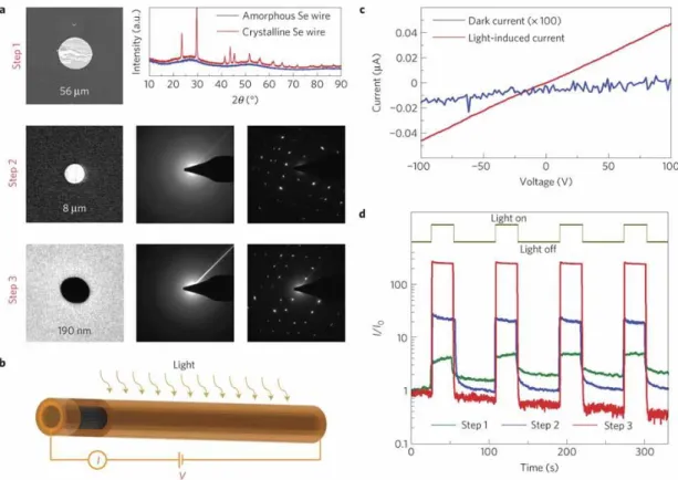
Figure 1.10: COMSOL Multiphysics simulation to show the change in the electric field, when a metal and dielectric approaches to each other. Here the TEFLON has a stable potential while Al electrode set as a floating potential connected to an external circuit. Gradually decrease in the floating potential correspond to charge flow from Al to external circuit because of the approaching potential. ... 21 Figure 2.1: a) A macroscopic multimaterial rod is reduced to ordered arrays of nanowires by thermal size reduction in a protective polymer matrix in successive steps. Each step starts with structures obtained from a previous step, resulting in geometrical size reduction and increment in wire number and length. Using the technique, we produced millions of kilometer-long nanowires with sub-10 nm diameter and an aspect ratio of 10. b) As an example, a 10 mm amorphous semiconducting rod (Ge–As–Se– Te) is reduced to hundreds of meters of single 200 μm wire (reduction factor ×50), ~30 wires of 5 μm diameter (reduction factor ×50) and ~1,000 wires of 250 nm (reduction factor ×50). Nanowire arrays are obtained as embedded in a dielectric polyetherimide encapsulation. Wire-array cross-sections with well-ordered wires and extracted, globally oriented slivers are shown after each step. Inset: Transmission electron microscopy image of a single 32-nm-thick nanowire obtained by further scaling down the third-step nanowires. ... 26 Figure 2.2: a) Amorphous selenium wires are crystallized through heat treatment or by exposing to the organic reagent pyridine. SEM images of regularly scaled-down individual selenium wires. The electrically conductive hexagonal crystallographic phase is obtained by X-ray and electron diffraction. b) A schematic representation of the photoconductance measurement geometry. c) The photoconductance from a selenium nanowire in the dark and on white-light illumination. d) A logarithmic increase in the ratio of photocurrent versus dark current (I/I0) and a reduction in
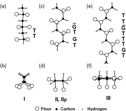
switching time (τ) with reducing nanowire diameter are observed. The performance increase is attributed to the high optical density of selenium, increased surface-area-to-volume ratio and enhanced scattering in the polymer matrix. ... 29 Figure 2.3: Application of fiber that produced by drawing technique. ... 30 Figure 2.4: Different crystal structure of PVDF. a-b) Piezoelectric form I chain TT structure. c-d) α-phase PVDF which can be polarized, but it doesn’t reveal any piezoelectric effect. e- f) Form III PVDF. ... 32 Figure 2.5: PVDF phase transformation mechanisms. Piezoelectric β phase can be obtained by several ways: quenching under high pressure from the PVDF solution,
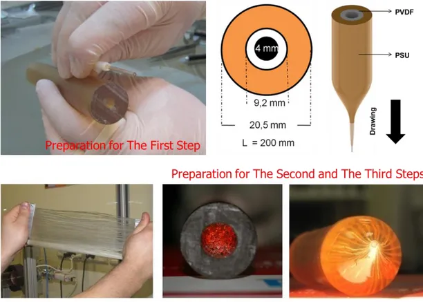
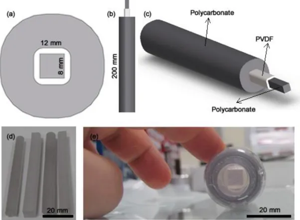
stretching α-phase PVDF (Generally 1 to 4 or more stretching result in high amount of phase transformation), and polarization of form one under electric field. We prefer to apply last option for phase transformation for out fibers because stretching may harm nanotube structure. ... 33 Figure 2.6: Preform consolidation process take place in a tubular oven at elevated pressure and moderate vacuum as shown in the right side. A successfully consolidated preform and the consolidator device shown at the left. ... 35 Figure 2.7: Structure of the first step preform and preparation of first step drawing were shown in the schematics. We roll PVDF thin films and directly insert in to the core of the preform. In the preparation for step 2 and 3 fiber drawing: We need to cut, clean and align the fibers before we start to the next step. We put first step fibers into a new preform and draw the fibers iteratively in order to produce nanotubes. ... 35 Figure 2.8: A custom made fiber tower, which is used to produce nanoribbon embedded fibers, consists of a preform feeding mechanism, furnace, thickness monitoring system, tension measurement unit, and a capstan. ... 36 Figure 2.9: Nanotube fabrication takes 3 iterative steps which results in different sizes. Size of a macroscopic rolled thin film reduced down to below 20 nm by using thermal reduction technique in a fiber tower. Rolled PVDF films inserted in the preform and as the preform shrinks at high temperature, PVDF melts and takes the shape of the preform in step 1. Nanotube arrays inserted in the preform scaled down by thermal drawing in step 2 and 3. ... 37 Figure 2.10: Square cross sectional PVDF nanoshell fabrication starts with preparing a square cross sectional macroscopic PC core. a-c) A 2 mm thick PVDF region obtained by rolling PVDF films around 8 mm thick PC square cross sectional core. Finally, PC rolled around the PVDF in order to create the cladding layer. Total thickness of the preform is 35 mm. d) 8 mm thick square cross sectional PC core extracted from a PC preform by using a milling machine. e) Preform consolidated under 1x10⁻² Torr vacuum at 186 oC for 35 minutes. ... 39 Figure 2.11: Square cross sectional PVDF nanoshell fabrication requires two fiber drawing process. As a result of first step drawing we obtain micro fibers and we put first step fibers in a second step preform and draw them again in order to obtain nanoshells. Although we have a single micro wire in first step, we can obtain a bundle
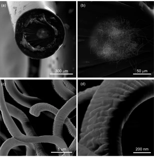
Figure 2.12: a-c) PVDF microtubes obtained by drawing a macroscopic preform in a fiber tower. Step 1 result in microtubes which are in a PSU jacket with diameter 50-50 μm and length longer than 100 m. Mechanically extraction of PVDF first step microtubes is possible. d-f) Step 2 results in micro and nanotubes which are also in PSU jacket with diameter 10 μm to 180 nm depends on the reduction factor. Not mechanically but chemically extraction of second step tubes is possible. g-i) Step 3, results in globally ordered tubes which can have diameter below 20 nm. ... 42 Figure 2.13: PVDF micro and nanotube cross-section scanning electron microscopy (SEM) images. Although, sample preparation is done by using cryotom, there is still a smearing effect which disturbs the image quality. Besides, polymer-polymer combined structure has shown not much contrast for SEM. a) A representative appearance of the PVDF. b) First step microtubes which have a diameter rage 30 to 200 μm. c) Second step nanotubes which have a diameter rage 100 to 700 nm. d-e) Third step nanotubes which have a diameter rage 20 to 100 nm... 43 Figure 2.14: PVDF nanoshells are produced by using two step fiber drawing process. a) First step fibers have a single square cross sectional microshell. Thickness of the PVDF shell is below 100 μm. c-d) PC cladding of the microtubes can be etched by using DCM. d-e) Second step drawing results in nanoshells. Unfortunately, nanoshells couldn't maintain perfect square cross sectional shape. f) Even though their cross sections are not perfectly square, adjacent positioning of chemically extracted nanoshells reveals that high density packing of square cross sectional PVDF nanoshells is still possible. ... 44 Figure 3.1: Transition into α, β, and γ phases from the molten state or other phases of PVDF are possible by using versatile processes. γ phase transition from the molten PVDF requires to combine specific processing conditions such as high temperature and high shear. Iterative size reduction by fiber drawing, which stands as a new method for nanotechnology, triggers the polar γ phase transformation by providing the two conditions concurrently. ... 48 Figure 3.2: SEM micrographs of PVDF nanoshells produced as a result of two iterative fiber drawing processes. (a) Photograph of meters-long as-drawn square cross sectional fiber. (b) The first step fiber drawing results in a single square cross sectional microshell in a fiber. Thickness of the PVDF shell is below 10 µm. (c) First step microshells after their Polycarbonate (PC) cladding was etched by using DCM. (d-e) The second step fiber drawing results in nanoshells having rounded square cross
sectional shape. (f) High density packing of chemically extracted PVDF nanoshells. ... 51 Figure 3.3: Results of the finite element simulation for the process of all-polymer fiber drawing. (a) The stress distribution in the preform drawn by a 3 MPa tensile stress. (b) Demonstrating the shear stress distribution which triggers γ phase transition in PVDF nanoribbons at high temperatures. ... 52 Figure 3.4: The fabrication steps of the PVDF ribbon embedded in PES preform which is a macroscopic copy of the final nanoribbons. As an initial step, (1) a PVDF preform is built by rolling PVDF sheets and (2-3) a slab is mechanically extracted out of the PVDF preform. (4-5) Next, the PVDF slab is inserted into a PES preform which is then sealed by heating in a consolidator oven. (6) The final multimaterial product turns into a PVDF ribbon embedded PES matrix. Dimensions and design specifications of the preform directly affect the size and shape of the final product of the drawing process. ... 54 Figure 3.5: A novel top-to-bottom nanofabrication technique for producing kilometer-long piezoelectric nanoribbons. An iterative fiber drawing scheme allows to achieve nanometer structures. A macroscopic PVDF slab is inserted, thermally sealed in a PES matrix, and drawn thermally to produce first step fibers. At high temperatures, molten PVDF flows together with softened PES cladding, producing tens of meters long PVDF microribbon encapsulated in PES. First step fibers are stacked and redrawn in a new preform for the second step fiber drawing in order to decrease the size of the ribbons down to nanometers. Further size reduction can be accomplished by following same stacking and redrawing cycles. From the first step to the last step, total number and length of the ribbons in the fiber increase as the size of each nanoribbon decreases. ... 55 Figure 3.6: SEM micrographs of PVDF micro and nanoribbons produced by using iterative size reduction technique in each drawing step. (a) Photograph of tens of meters long PDVF nanoribbon array embedded in PES cladding. (b) Cross sectional image of first step PVDF microribbon in the PES cladding. Inset: Free-standing PVDF microribbon obtained by etching PES cladding using chemical etchants. (c) Cross sectional image of second step fiber with ~400 nanoribbons. Inset: Close-up image of nanoribbons. (d) Lateral image of second step nanoribbons. Inset: Close-up image of
fiber. Close-up image of a single bundle. (f) SEM of third step nanoribbons extracted out of their cladding. Inset: Close-up image of aligned nanoribbons. ... 57 Figure 3.7: (a) Cross sectional SEM images of the second step nanoribbons embedded in PES fiber prepared by breaking just after liquid nitrogen cooling. (b) PVDF nanoribbons are extracted out of the PES cladding due to uniaxial pulling force for breaking the fiber. (c) A preferential buckling is observed due to the rectangular cross sectional shape of the nanoribbons. (d) A closer look at the PVDF nanoribbons proves that ribbon shape is perfectly preserved. ... 58 Figure 3.8: Mean of size distribution in nanoribbon width is calculated from SEM images as <w> = 309 nm. Standard deviation of size distribution is σ = 35 nm. Standard deviation normalized with respect to the mean is σ / <w> ≈ 11 %. ... 59 Figure 3.9: Dark field optical microscopy of a fourth step fiber containing sub-nanometer millions of PVDF ribbons. The sub-sub-nanometer ribbons can’t be extracted by etching PES cladding, but dissolved in DCM. Bundles can be seen clearly under optical microscope. ... 60 Figure 3.10: XRD and ab initio simulation results representing γ phase transition from PVDF slab via fiber drawing process. (a) PVDF has three main forms which are known as nonpolar α phase, polar β and γ phases. (b) XRD data of PVDF slab extracted from a preform, microribbon and nanoribbon are taken after removing the PES cladding. Peaks observed at 18.5o and 18.6o, 20.1o and 20.3o, 26.8o correspond to the planes of γ
polar form (020), (002)/(110) and (022), respectively. α phase peaks at 17.7o 26.5o and
27.8o are collected from (100), (021) and (111) planes. Peak at 20.8o, is the only β peak observed in the slab. Spontaneous polar form (γ phase) is achieved after the thermal size reduction in all fiber drawing steps. (c) ATR-FTIR peaks from the first, second and third step PVDF microribbons and nanoribbons representing α and γ phases. 833, 840, 885, 1234, 1279 and 1286 cm-1 are characteristics of the γ phase PVDF. 615, 763, 796, 854, 870, 973, 1146, 1210 and 1383 cm-1 are the FTIR peaks of α phase PVDF. Fraction of the γ phase is 74 % in first step microribbons whereas it decreases 72 % in third and second step nanoribbons. (d) XRD patterns showing the characteristic peaks of the second step PVDF nanoribbons at different annealing temperatures. Although the temperature is increased above the melting point of PVDF, dominance of γ phase is obvious from the peaks at 18.6o, 20.1o and 26.8o positions. (e) Transition from α (yellow circle) to γ phase (blue triangle), (f) transition from β (red square) to γ phase with compressive strain and (g) transition from α to β phase with tensile strain on the
unit cell with 6 monomers of PVDF in axial direction are simulated considering fiber drawing parameters (high temperature and shear stress) using ab initio calculations. 0
oK results are corresponding to the case where temperature effects are excluded. .... 62
Figure 3.11: Ab-initio calculations reveals that, with the compressive strain in axial direction, alpha and beta PVDF transforms into gamma PVDF both for 0K and 470
oK. The required compression for the transformation from alpha to gamma at 0K is
10.8% and from beta to gamma is 13.4%. The required compression decreases to 3% and 8% at 470 oK... 65 Figure 3.12: Finite element simulation of the temperature distribution in the furnace. The height of the heating zone is 2.5 mm and the temperature of the PVDF in the core is around 470 oK. ... 67 Figure 3.13: Ab initio calculations for explaining phase transformation at higher temperatures. Increasing the temperature decreases the required strain for phase transformation accordingly. (a) Transition from α (yellow circle) to γ phase (blue triangle), (b) transition from β (red square) to γ phase with compressive strain and (c) transition from α to β phase with tensile strain. ... 68 Figure 3.14: Experimental setup for piezoelectric characterization of the PVDF nanoribbons. ... 70 Figure 3.15: (a) AFM topography of 80 nm thick and 180 nm wide single and double nanoribbons on a metal coated substrate. (b) Hysteresis loop of as produced single nanoribbons at 25 V and 100 Hz which represents the spontaneous electric polarization. (c) Displacement-voltage hysteresis loop taken by an AFM and piezoelectric evaluation system from a single PVDF nanoribbon. Inverse butterfly loop is a characteristic result of the negative d33 piezoelectric coefficient. Total measured
displacement is a function of 𝐸 and 𝐸2. Since the applied electric field and displacement are known, 𝑑33 and 𝑄 values can be calculated in least square sense. Data fitting is executed by using 370 data points. ... 71 Figure 3.16: COMSOL Multiphysics simulation for understanding the characteristic of the displacement induced via tip indentation. In model design, AFM tip assumed a sphere (D=10 nm) and the temperature kept constant at 295 K. In order to make a mechanical contact on the surface of the PVDF nanoribbons, we set the AFM control loon on and apply a –60 nN which generate maximum 0.3 nm elastic deformation on
Figure 3.17: COMSOL Multiphysics simulation for understanding Joule Heating phenomena in 80 nm thick PVDF nanoribbons. In model design, AFM tip assumed a sphere (D=10 nm) and the temperature kept constant at 295 oK. (a) Electric potential distribution between conductive AFM tip with a 30 V applied voltage and grounded surface. (b) Since Joule Heating proportional to i2R (i is the current traveling between electrodes, R is the resistance), there is no temperature change observed in nanoribbons as a function of electric field. ... 75 Figure 3.18: Fabrication process for the device produced using first step microribbons. (a) A 50 µm thick microribbon embedded single fiber is selected. (b) The fiber is longitudinally divided in two pieces. (c) The surface of the piece with the ribbon trapped is coated 50 nm gold. (d) After carving the PVDF microribbon out of the cladding, it is cut in equal pieces. (e) One side coated microribbons are aligned on a silicon substrate. Next, Ag paste and Cu wire electrodes are attached on the gold coated surface of the microribbons. (f) The structure is transferred onto a PDMS layer. (g) The back side of the PVDF microribbons are also coated with 50 nm gold and the whole device is embedded in PDMS. ... 78 Figure 3.19: Design of the device using PVDF nanoribbons.50 nm gold is sputtered using a shadow mask on the surface of a PVDF nanoribbon layer which is extracted out of the PES cladding in a DCM solution. ... 79 Figure 3.20: Impedance measurement of the piezoelectric devices modeled as a parallel R-C circuit in order to determine internal capacitance and resistance of (a) the device produced using microribbons and (b) the device produced using nanoribbons. Experimental results data are perfectly fitted with simulation. ... 80 Figure 3.21: Voltage and current outputs of the devices are tested under quasi-periodic tapping forces. Output intensity is related to the applied tapping force magnitude and frequency. (a) The device produced with 50 µm thick microribbons has an output current up to 3 µA and (b) voltage up to 7 V. (c) The device produced with 300 nm thick nanoribbons has an output current up to 10 µA and (d) voltage up to 60 V. .... 81 Figure 3.22: Voltage and current outputs of the devices are tested under quasi-periodic tapping forces. Output intensity is related to the applied tapping force magnitude and frequency. (a) The device produced with 50 µm thick microribbons has an output current up to 3 µA and (b) voltage up to 7 V. (c) The device produced with 300 nm thick nanoribbons has an output current up to 10 µA and (d) voltage up to 60 V. .... 82
Figure 3.23: We produced a device with identical structure using non-piezoelectric amorphous As2Se3 nanowires instead of PVDF nanoribbons in order to confirm that
the measured peaks are result of a piezoelectric response. ... 83 Figure 4.1: Polymer slabs we produced in a directional press under 30 Bar pressures using 3 pieces Al mold. Cold pressing doesn’t result in a homogenous consolidation of the polymer powders as shown in inset. Elevating the temperature up 90 °C results in a perfectly homogenized and air bubble free slab... 88 Figure 4.2: A schematics explaining the iterative fiber drawing technique. PVTF corresponds to PVDF-TrFE. In the first step fiber drawing process, a macroscopic slab diminished down to micro scale by the help of applied temperature and stress. Inset SEM pictures were taken from the first step ribbons; i is the cross sectional SEM image of the first step fiber and the scale bar is 50 µm. ii and iii are the SEM pictures of micro ribbons after the cladding was etched. The scale bars for ii and iii are 1 mm and 100 µm, respectively. The first step micro fibers were stacked and inserted in a new PES preform and redrawn. Inset SEM pictures were taken from the second step ribbons; iv is the cross sectional picture of the nanoribbon array and the scale bar is 50 µm. v and vi were taken after the cladding was etched. Inset picture vi was taken from a single ribbon and conservation of the ribbon shape is clear in that picture. Scale bars of inset figure v and iv are 25 µm and 5 µm, respectively. Since there is 3:10 ratio between thickness and the width of the ribbon, a ribbon with 1 µm in width has 300 nm thickness. ... 89 Figure 4.3: XRD measurements from the first and the second step ribbons. a) Phase transformation with respect induced deformation was observed in preform. Increasing deformation also increases the orientation as well as the crystallization in piezoelectric form. Increasing trend in the peak heights showing the ratio of crystallization. Shift in the peaks trough the lower diffraction angels correspond to increase in the d space between planes and enhancement in orientation. b) The first step fibers were already exposed to high deformation and temperature was redrawn in the second following process. Since redrawing can be considered as secondary heat treatments, there is a slight relaxation was observed in molecules. On the other hand, orientation (200) / (110) drastically increased. Nanoribbons discloses better piezoelectric properties because they have higher surface area, less impurities and defect, and better
Figure 4.4: Detailed analysis of XRD results. a-c) Peaks at 20°, 41° and 35° shifts to lower diffraction angles with respect to increasing deformation percentage. Besides, increase in the deformation increase in the nucleation in (200) / (110) direction. d-c) This effect also causes a drastic increase in d space between crystal planes, and simply corresponds to better chain orientation and polarization. Although deformation ratio was increased the d space in the first step drawing, chains are relaxed and d space distance slightly decreased in the second step process. g-c) Increase in the orientation can be detected by calculating the relative intensity of the peaks. In XRD characterization technique highest peak always should be taken as the 100 % peak and the relative intensity of the other peaks calculated with respect to the highest peak. We clearly see that, peak for (200) / (110) diffraction planes were constant and the highest in the first and the second step. On the other hand increasing deformation and drawing steps decreases the peak intensity for the other diffraction planes. That means, orientation of the polymer chains and the nucleation of the crystals were increased through (200) / (110) orientation, while the orientation in the other directions were decreased. This effect proves that the dipole orientation and chain orientation became more homogenous with increasing deformation ratio. ... 94 Figure 4.5: Orientation and nucleation were increased in (200) / (110) direction with increasing deformation. Confirming that change in the crystallinity with respect to deformation ratio also shows that there is an increasing trend with respect to increasing deformation ratio. Since, only 13 % of the slab was crystalline, it was increased to 80 % after fiber drawing process. In the second step fiber drawing, crystallinity was decreased to 77 %... 95 Figure 4.6: a) FTIR measurements from the first and the second step ribbons showing that induced β phase also confirms XRD results. The bands at 505, 840, 843, 1285, and 1429 cm-1 corresponds to β phase. b) Alignment of the polymer chains with respect to fiber drawing axis was also investigated using parallel and perpendicularly polarized infrared light. Measurements reveals that, as shown in the inset, polymer chains and dipoles were aligned parallel and perpendicular to fiber drawing axis, respectively. 96 Figure 4.7: Ab initio simulations was conducted to understand phase transformation dynamics in fiber drawing process. Since the orientation of the molecules was unknown before fiber drawing, the both compressive and the tensile strain considered, which take place during fiber drawing in the necking region of the preform. We started by optimizing the α-PVDF-TrFE and we applied tensile strain. 13 % tensile strain was
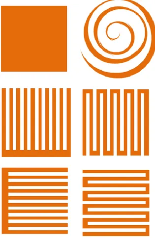
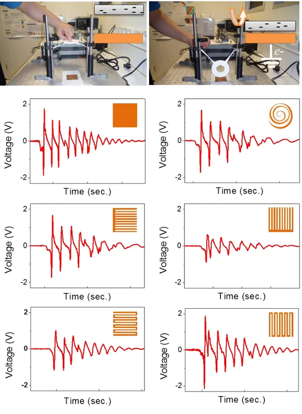
enough to obtain a perfect β-PVDF-TrFE. Compared to ground state calculation, which ignores temperature effect, applied temperature decreases the energy barrier for phase transformation. Applying compression on β- PVDF-TrFE, relaxes the system with and without temperature. Similarly, α-PVDF-TrFE was destroyed, when a compressive strain was applied. ... 98 Figure 4.8: Piezoelectric measurements was performed from a 300 nm thick single nanoribbon. Before the measurements, position of the nanoribbon was located using non-contact surface scanning techniques. ... 100 Figure 4.9: Volumetric displacement with respect applied voltage was used to characterize charge constant of as produced PVDF-TrFE nanoribbons. ... 101 Figure 4.10: Frequency dependent power measurements of the device made by nanoribbons. ... 102 Figure 5.1: Detailed images of chalcogenide based 3D printed MULTENG energy harvesting device and its layers. a) An illustration of 3D printed MULTENG energy harvesting device which consists of 6 alternating polymer and chalcogenide layers. a-1) Representation of layers which consist of PEI nanopillars. a-2) SEM image of PEI nanopillars. Scale bar is 1 µm. a-3) Higher magnification SEM image of PES nanopillars. Scale bar is 250 nm. a-4) Photograph of MULTENG device fabricated with 3D printing method. a-5) Representation of layers, which consist of F-As2Se3
core-shell nanostructure. a-6) SEM image of F-As2Se3 core-shell nanostructures. Scale
bar is 25 µm. a-7) Higher magnification SEM image of F-As2Se3 core-shell
nanostructures. Scale bar is 500 nm. b) Working mechanism of the MULTENG that utilizes the contact mode triboelectrification with external electronic flow in short circuit condition. 1. Motion of MULTENG from original state to charge generation state. Sharing charges & Positive peak current generation (current flow) in unit 1 of MULTENG. 2. Sharing charges & Positive peak current generation (current flow) in unit 3 of MULTENG. 3. Sharing charges & Positive peak current generation (current flow) in unit 2 of MULTENG. 4. Full Contact position. 5. Separation of layers and sharing charges & Positive peak current generation (current flow) in unit 2 of MULTENG. 6. Separation of layers and sharing charges & Positive peak current generation (current flow) in unit 3 of MULTENG. 7. Separation of layers and sharing charges & Positive peak current generation (current flow) in unit 1 of MULTENG. 8.
Figure 5.2: Initial measurement setup in order to obtain the best material couple to obtain highest output values. b) Image of the samples that were investigated for material selection measurements. c) Tapping device with a 5V DC motor, which gives the mechanical power in order to achieve voltage and current characteristics. ... 109 Figure 5.3: Left column: Contact and separation of MULTENG under tapping force. Right column: finite element model of mechanical response of MULTENG which perfectly matches with real behavior of MULTENG. ... 113 Figure 5.4: Detailed sketches and dimensions of MULTENG. a) Cross section of multi layered structure. b) Side view, c) and top view of the MULTENG. d) Cross section of layers of MULTENG. e) Bottom view, f) and side view of layers of MULTENG. ... 115 Figure 5.5: Detailed representation of a) PEI nanopillar decorated and b) As2Se3
nanostructure transferred films. Bottom of the PEI film was coated with Aluminum (Al) using thermal evaporation while As2Se3 nanostructures were directly deposited
on the Al tape. Copper (Cu) tapes were attached to both of the film in order to provide conductivity. ... 116 Figure 5.6: Fabrication process of PEI nanopillars. a) AAO membrane is used as supported on its aluminum (Al) substrate. b) Dissolved PEI film is drop casted on the AAO template. c) Polymeric film is peeled off from the template after solvent evaporation process. ... 116 Figure 5.7: a) As2Se3 rod was synthesized by sealed quartz ampoule method and then
the material is inserted in a rotating machine. It transformed from rod to the tube shape by using centrifugal force. b) As2Se3 tubes after extracting from quartz ampoule by
cracking and uniformly etching the quartz ampoule. c) The photograph of rotating machine. ... 117 Figure 5.8: Synthesis of chalcogenide glass tubes. Three steps process (a) collection of materials, (b) material purification and sealing, (c) rocking and homogenization. ... 118 Figure 5.9: A model shows iterative size reduction technique. Macroscopic core of the preform shrinks into microscopic fibers in the first step size reduction process. In the following size reduction steps, size of the cores decreases down to nanoscale and the total length increases up to kilometer range. Iterative drawing occurs by putting first step fibers into the core of the second step preform, putting second step fibers into third step and drawing consecutively. ... 119
Figure 5.10: Cross-sectional and longitudinal SEM images a) first step, b) second step, c) third step PES-As2Se3 core-shell structures. ... 120
Figure 5.11: Fluorination process of the As2Se3 nanostructures. As2Se3 nanostructures
are immersed into the FDTS solution. Finally, nanostructures are washed to remove free FDTS ligands and are produced as monolayer protected. ... 121 Figure 5.12: Measurement setup for tapping frequency dependent characterization of MULTENG. a) Experimental setup. b) Detailed representation of open circuit voltage measurement tools. c) Detailed representation of short circuit current measurement tools. ... 123 Figure 5.13: Open circuit characteristics and real-time performance of the MULTENG based on the tapping frequency. a) Frequency dependent open circuit voltage and b) short circuit current measurements. c) Frequency dependent instantaneous power and power density measurements. Rectified d) open circuit voltage and e) short circuit current measurements. f) Frequency dependent DC power analysis. Inset shows the time dependent behavior. g) Detailed plot of single OCV peaks in different frequencies which shows obtained outputs with respect to contact and separation sequence of different units of MULTENG. Orange, blue and green arrows correspond to motion in unit 1, unit 2 and unit 3 respectively. h) Frequency dependent efficiency that was obtained from open and short circuit measurements. i) Captured image of 38 flashing LEDs powered by MULTENG. j) Image of 38 enlightened LEDs by the stored energy in the harvesting circuit. k) Schematic representation of the energy harvesting circuit. ... 124 Figure 5.14: Linear relation between tapping frequency and tapping power of tapping machine. ... 125 Figure 5.15: Single peak a) OCV and c) SCC plots at different frequencies. c) Expanded OCV representations which show the contact and separation of different units of MULTENG. ... 127 Figure 5.16: Stability test for current response of MULTENG with random time scales and various frequency. ... 128 Figure 5.17: Finite element simulation results to understand the change in the induced potential in accordance with the motion of the layers. a) Representation of simulation setup. b-e) Initially, outer layers come in contact (first unit 1 and then unit 3) and
come in contact as well. i) Comparison of between measurement from a single layer generator and our analytical model which simulates the open circuit voltage generation. ... 130 Figure 5.18: Schematics of single layer triboelectric device. ... 132 Figure 5.19: Electrical characterizations of MULTENG, activated from the motions of a moving car. a) Schematic representation of driving route in the university campus. Inset shows the squeezed MULTENG in full contact position. Inset shows the bump dimensions on the route. b) Instantaneous power and power density measurements as a function of car velocity. c-h) Open circuit voltage and short circuit current measurements with respect to car velocity. Orange, blue and green colors corresponds to single, double and triple contact and separation in different units of MULTENG, respectively. ... 135 Figure 5.20: Single, double and triple peaks in a sequence were correspond to successive linear contact and separation of different units of MULTENG as a response to car vibration. ... 137 Figure 5.21: Single, double and triple peaks in a sequence were correspond to successive angular contact and separation of different units of MULTENG as a response to car vibration. ... 138 Figure 5.22: Electrical characterization of acoustically excited MULTENG. a) Schematic representation of sound excitation. b) Sound frequency dependent instantaneous power and power density measurements. Inset: Change input sound frequency (Hz) over time. Sound frequency dependent c) open circuit voltage and d) short circuit current measurements. e) Rectified open circuit voltage and single peak open circuit voltage. f) Rectified short circuit current and single peak short circuit current. ... 139
List of Tables
Table 1.1: Comparison between the piezoelectric coefficient of PVDF, PVDF-TrFE and other ceramic piezoelectric materials. PVDF and PVDF-TrFE nanoribbons have the highest piezoelectric coefficient among other reported measurements from those polymers and ceramic piezoelectric materials. *ISR: Iterative Size Reduction. **PZT: (PbxZrx-1Ti)O3 ***PVD: Physical Vapor Deposition. ... 3
Table 1.2: Comparison of the recently-developed triboelectric generators made of different materials, with respect to their open circuit voltages, short circuit currents, output voltage, working mechanisms and working frequencies. ... 6 Table 2.1: Unit cell parameters, space group numbers and molecular chain data for all of the phases of PVDF. ... 32 Table 3.1: Comparison of PVDF nanowire production techniques considering as-produced nanowire properties in terms of aspect ratio, uniformity, size and geometry control, multimaterial production compatibility, yield and device integration ... 50 Table 3.2: Comparison of the piezoelectric coefficients of γ-phase PVDF structures. ... 84 Table 4.1: Comparison between key properties of piezoelectric polymer structures 87 Table 4.2 : A detailed list of XRD results from the first and the second step piezoelectric ribbons explaining the relation between relative intensity and change in the d space for explaining the orientation direction. ... 92 Table 4.3: Total energy of most symmetrical α-PVDF-TrFE with respect to FS configuration. ... 98 Table 4.4: Comparison of PVDF-TrFE nanostructures in terms of fabrication methods and the piezoelectric charge coefficient. ... 103 Table 5.1: Triboelectric materials are listed according to their triboelectric polarity ... 106
Table 5.3: List of parameters used in our model to calculate open circuit voltage. 132 Table 5.4: Summary of experimental results. Obtained maximum outputs from tapping, automobile motion and sound excitation applications, respectively. ... 141 Table 5.5: Comparison of the triboelectric contact-mode device performances. .... 142
Chapter 1
Introduction
Developments led by materials science and engineering have revealed the importance of flexible electronics [1]–[7]. Organic solar cells, flexible displays and cameras, artificial skin, smart surfaces and transistors were recently demonstrated on circuitries made by flexible components [1], [8]–[10]. Fabricating high efficient flexible devices with multi-functionalities requires using different types of materials such as conductive polymers, semi-conductive self-assemble films and resistive layers [7], [11], [12]. Although conventional electronic materials represent very high electronic performances, integration and fabrication of circuits on flexible, stretchable and curved surfaces is not an easy task. Especially, interfacing electronic devices with organs and living tissues requires non-invasive, flexible and multi-functional devices. Transmitting light and electric signals through the brain and other organs for recording real time information from organs can be possible by using flexible electronic and soft electronic fiber devices [13]–[17]. Fabricating all polymer flexible electronic devices seems more promising and inexpensive, where there is a greater demand for developing new organic high performance materials in terms of electronic properties such as mobility, conductivity and piezoelectricity. Researchers study on improving the performance of organic materials such as conductive inks, sheets and semiconductors by playing size, shape and composition of used organic substances [18], [19]. In addition to these organic materials used in flexible electronics, there is an emerging need to develop organic piezoelectric materials that can be used in many different applications such as energy harvesting, sensing and actuation, artificial skin
This thesis focuses on two main subjects, piezoelectricity and triboelectricity. In the first part, we developed nanoribbons from Poly (vinylidene fluoride) (PVDF) and its copolymer Poly (vinylidene fluoride)-co-tri (fluoroethylene) (PVDF-TrFE).
Although recent articles were reporting that PVDF was not compatible with fiber drawing process for obtaining polar phase nanostructures [11], we proved that γ polar phase PVDF can be spontaneously induced during the fabrication of PVDF nanoribbons via fiber drawing. Furthermore, we obtained the highest piezoelectric coefficient from our nanoribbons in comparison with the reported values in the literature. Table 1.1 represent a detailed analysis of the piezoelectric coefficient of polymer and ceramic piezoelectric materials with respect to their shapes, phases, fabrication methods and post-processing techniques. The highest reported piezoelectric coefficient was -7 pm/V from pure γ phase PVDF/Clay nanocomposites produced by solution based methods without requiring and post-processing such as polarization under high electric field [26]. Our γ phase PVDF nanoribbons, which doesn’t require any post processing for obtaining polar phase, represent 8.35 times higher piezoelectric coefficient (-58.5 pm/V). The piezoelectric coefficient of the γ phase PVDF can be increased by shaping it in nanoribbons and mixing the phase composition with the β phase PVDF. So, the reported highest piezoelectric coefficients for β/γ mix-phase PVDF nanoribbons and thin films are 16.02 pm/V and 10.62 pm/V, respectively. This reported values were still far behind of our results [22]. There are several reasons that we obtained a very high piezoelectric coefficient: (1) non-clamping boundary conditions are valid for nanoribbons in the piezoelectric characterization, which means that the measured piezoelectric coefficient corresponds to effective piezoelectric coefficient; (2) nanoribbons are produced using a solvent free fabrication technique and display better piezoelectric properties.
Piezoelectric characterizations of nano-scale objects are extremely challenging. There are two basic techniques for measuring piezoelectric coefficient of materials: direct and indirect measurements, which are based on the applied force and the applied electric field, respectively. The indirect measurement techniques are very useful for characterizing piezoelectric properties of nano-materials. In this type of measurements, the displacement of the material with respect to the applied electric
field can be measured using very precise displacement sensors such as laser beam interferometers or atomic force microscopy, which have angstrom level sensitivity.
Table 1.1: Comparison between the piezoelectric coefficient of PVDF, PVDF-TrFE and other ceramic piezoelectric materials. PVDF and PVDF-TrFE nanoribbons have the highest piezoelectric coefficient among other reported measurements from those polymers and ceramic piezoelectric materials. *ISR: Iterative Size Reduction. **PZT: (PbxZrx-1Ti)O3
***PVD: Physical Vapor Deposition.
Material Phase |𝒅𝟑𝟑| (pm/V) Type Method Poling Reference
PVDF γ 58.5 Nanoribbon ISR* No Our Study
PVDF β / γ 16.02 Nanoribbons Template Yes [27]
PVDF β / γ 10.62 Thin Film Solution Yes [27]
PVDF γ 7 Nanocomposite Solution No [26]
PVDF β 57.6 Nanowire Electrospinning Yes [28]
PVDF β 33 Thin Film Stretching Yes [29]
PVDF β 8 Nanowires Template No [30]
PVDF β 6.5 Nanowires Template No [31]
PVDF-TrFE β 384 Nanoribbon ISR No Our Study
PVDF-TrFE β 72.7-210.4 Nano-grass Template Yes [32]
PVDF-TrFE β 48 - 81 Nanoribbons Template Yes [33]
PVDF-TrFE β 13 – 19 Thin Film Solution Yes [33]
PVDF-TrFE β 25-45 Nanowire Template No [34]
PVDF-TrFE β 16-23 Thin Film Solution No [34]
PVDF-TrFE β 22 Nanowires Template No [30]
PVDF-TrFE β 8 Nanowires Template No [31]
**PZT Perovskite 200 Thin Film Sol-Gel Yes [35]
PZT Perovskite 145 Nanoribbon Lithography Yes [36]
PZT Perovskite 90 Nanoshell Template Yes [37]
PZT Perovskite 80 Nanowire Sol-Gel Yes [38]
PZT Perovskite 50 Nanowire Sol-Gel Yes [39]
PZT Perovskite 17 – 26 Powder Sol-Gel Yes [40]
ZnO c-Oriented 110 Thin Film ***PVD No [41]
ZnO c-Oriented 14.3 – 26.7 Nanoribbon PVD No [42]
ZnO c-Oriented 7.5 Nanopillar Template No [43]
NaNbO3 Orthorhombic 0.85-4.26 Nanowire Solution Yes [44] KNbO3 Orthorhombic 3 – 13 Nanowire Solution Yes [45] BaTiO3 Single Crystal 16.5 Nanowire Solution Yes [46]
GaN Wurtzite 12.8 Nanowire Solution Yes [47]
However, in the study by Pu, J, et al. [28], the authors reported a high average piezoelectric coefficient (57.6 pm/V) from β phase nanowires produced by
the authors used a very primitive measurement technique based on optical microscopy observation for measuring piezoelectric coefficient of a single nanowire, with ~20% accuracy. Basically, they measured the bending of a suspended nanowire with respect to the applied bias using a calibration background. Therefore, it can be concluded that such technique is not very convenient for nano-materials, as it does not include many influencing factors, such as mechanical vibrations, thermal effects and electrostriction. When these effects are considered, their d33 coefficient will dramatically decrease. For
instance, when the electrostriction effect was ignored in our study for the piezo-response of PVDF nanoribbons, the measured piezoelectric coefficient increases up to -72.8 pm/V, which doesn’t reflect pure and real piezo-response. Therefore, the determination of piezoelectric properties of nanomaterials requires high precision evaluation of the measured data as well as very sophisticated instruments. So, we performed a very precise quantitative piezoelectric characterization technique using AFM as a sensitive displacement sensor and Radiant Premier II as a piezo-evaluation system. Before the nanoribbon measurements, we confirmed our measurements using a commercial PVDF film. In addition, we considered the other parameters (ferroelectric, ferroelastic, electrostriction, and dilatation) which can influence the quantitative evaluation of piezoelectric measurement. For instance, we calculated the indentation of AFM tip (0.3 nm) under 60 nN the applied force by conducting a COMSOL simulation. Besides, the thermal effects were also simulated. Ferroelastic motions can be ignored due to constant local contact loading during the measurements as shown by the finite element simulations in Chapter 3. The value of the piezoelectric coefficient (d33) was calculated by a theoretical fitting to the experimental data, which
is explained in Chapter 3. We concluded that 87.4 % of the deflection resulted from pure piezoelectric effect and 12.6 % of the deflection is a result of electrostriction, which corresponds to -58.5 pm/V effective average piezoelectric coefficient measured with 76 % accuracy. PVDF nanoribbons can be considered as potential replacement to the lead-based and lead-free piezoelectric ceramic materials. Although the lead-based (PbxZrx-1Ti)O3 (PZT) systems can represent better piezoelectric coefficients and
known as the most favorable ceramic piezoelectric material, they contain plenty amount of Pb. According to Restriction Hazardous Substances Directive (RoHS), Pb was banned from usage in household, consumer, IT-telecommunication, lightning, electronic, medical, etc. equipment, because it is extremely toxic. So, a new research area was appeared as “lead-free piezoelectric”. However, the performance of the lead-
free piezoelectric materials such as ZnO, NaNbO3 KNbO3 BaTiO3 and GaN still
suffers [42]–[47]. Therefore PVDF nanoribbons are a perfect candidate for the replacement of ceramic piezoelectric materials.
A copolymer of PVDF, PVDF-TrFE was considered as a better piezoelectric material due to extra fluorine in its molecular structure. Extra fluorine increases the polarization and the dipole moment, thus causes a direct nucleation in β phase as explained in Chapter 4. We obtained the highest piezoelectric coefficient (-384 pm/V) from PVDF-TrFE nanoribbons ever measured, as shown in Table 1.1. In the reference [32], the researchers achieved to obtain -72.7 pm/V piezoelectric coefficient from PVDF-TrFE nano-grass structures before polarization under electric field. After the polarization of the structures they obtained -210.4 pm/V piezoelectric coefficient. However, they performed this polarization process using an atomic force microscope tip on a single grass nanostructure and could not show any practical application with this piezoelectric structure. In the references [33] and [34], nanoribbons and nanowires were produced using the solution based template methods, yielding piezoelectric coefficients up to 81 pm/V. Despite the researchers could achieve higher piezoelectric constants in PVDF-TrFE thin films [34], compared to the PVDF [28], they could not beat the ceramic piezoelectric materials [41], particularly PZT [35]–[39]. Among these results obtained from PVDF, PVDF-TrFE, PZT and other ceramic nanostructured piezoelectric materials, our PVDF-TrFE nanoribbons apparently displayed the highest piezoelectric coefficient (-384 pm/V) without requiring an electrical polarization process, due to high stress and high temperature during the fabrication.
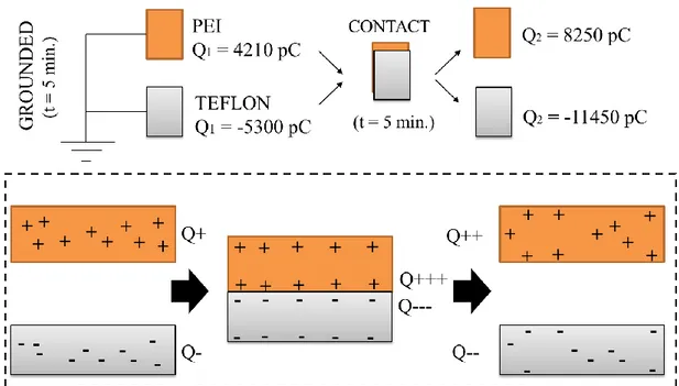
In the second part of the thesis, a triboelectric generator working in contact mode was developed, displaying a very high short-circuit current and output power, in comparison to the recent literature on the contact mode triboelectric generators (
Table 1.2). Such performance was achieved using surface fluorination, in order to achieve very high surface charge, in analogy to TEFLON, which is known as the highest negatively charged triboelectric material. However, the processing and surface modification of TEFLON are challenging and require costly processes. Here, we characterized a wide range of materials to understand their triboelectric responses with respect to their chemical content. We concluded that increasing fluorine content in
also showed that the inter-metallic semiconductor As2Se3 can be used as a triboelectric
material. Such devices can generate up to 396 V and 1.62 mA open circuit voltages and short-circuit currents, respectively. They can power up to 38 commercial LEDs, detect low frequency acoustic signals (10 - 100 Hz) and can be excited by small vibrations in a moving car. Hence our devices can be utilized as pocket-size power generators in future nano-electronic devices, and can also be used for vibration and acoustic detection.
Table 1.2: Comparison of the recently-developed triboelectric generators made of different materials, with respect to their open circuit voltages, short circuit currents, output voltage, working mechanisms and working frequencies.
Material Set Working
Mode Voltage (V)
Current
(mA) Power (W)
Working
Frequency Reference
PEI / F- As2Se3 Contact 396 1.600 0.51000 Low Our Study
TEFLON/Al Contact 215 0.66 0,14190 Low [48]
PDMS/Al Contact 232 0.0165 0.00382 Low [49]
TEFLON/Al Contact 100 0.0016 0.00016 Low [50]
TEFLON/SiO2 Contact 88.0 0.0610 0.00530 Low [51]
TEFLON/Cu Contact 72.0 0.0320 0.00230 High [52]
TEFLON/TiO2 Contact 21.3 0.032 0.00068 Low [53]
TEFLON/Cu Sliding 850 3.0000 1.50000 High [54]
PVC/Al Sliding 800 0.0337 0.02700 Low [55]
TEFLON/Al Sliding 250 0.250 0.06250 Low [56]
Since, As2Se3 is compatible with the iterative fiber drawing technique and has no
toxic reactivity, we rather preferred to use As2Se3 in the nanowire form, after the
fluorination process. A quick comparison of this study with the previous works on 3D integrated multilayer generators reveals that the power output of our devices is significantly high (Table 1.2), even in comparison to TEFLON. For example, Peng Bai, et al. [48]built a multilayer generator. Although some of the materials (TEFLON, Kapton, Al) that they used in their device were similar with the materials used in this study, the maximum output of their device (215 V and 0.66 mA, powered 9 LEDs) is very low when compared with the output here (396 V and 1.616 mA, powered 38 LEDs).
1.1. Piezoelectricity
Piezoelectricity is an important natural phenomenon which is extensively utilized by a myriad of applications in the field of sensing [57], [58], actuation [59]–[61], and energy harvesting [22], [62]–[64], where a transformation between mechanical and electrical energy is inherently required. Piezoelectricity can be observed in various materials including biological substances [65], [66], but only some of ceramics and polymers are considered to have high piezoelectric coefficients enough to be useful [22], [64], [67]. Besides, a closer look into applications of piezoelectricity such as bio-sensing, pressure bio-sensing, energy generation, artificial muscle and skin discloses that not only high performance piezoelectric, but also flexible, lightweight, and biocompatible materials are demanded [22], [68]–[72]. In addition, intriguing alternative production methods for these piezoelectric materials with advantageous post-processing integration steps are needed to be developed or devised in order to circumvent the main barrier before their large scale exploitation. Although many ceramic materials are known to be good piezoelectric, they suffer from high brittleness, low cyclic endurance, high processing temperatures, and high production cost as well as toxic elemental composition [73]. On the other hand, having none of these drawbacks, piezoelectric polymers such as Poly(vinylidene fluoride) (PVDF) are promising candidates for the replacement of ceramic piezoelectric materials, due to their high piezoelectricity, flexibility, and chemical resistance [22], [74], [75]. A simple evaluation through the literature about PVDF reveals that the form of nanowire brings on many advantages such as higher piezoelectric coefficient, higher electro-mechanical coupling efficiency, and better electro-mechanical properties in contrast with the form of thin films [22]–[24], [76]. The prominent processes for the production of PVDF nanowires are all solution based and they are not superior in all properties considering aspect ratio, uniformity, geometry control, yield, and large area device integrability. The challenging problems confronted in the field can be solved by introducing fundamental changes, starting from the fabrication technique.
1.1.1. Piezoelectric Effect