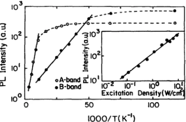
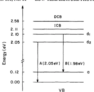
Solid State Communications, Vol. 101, No. 11, pp. 797-799, 1997 0 1997 Elsevier Science Ltd Printed in Great Britain. All rights reserved 0038-1098197 $17.00+.00 PII: s0038-1098(96)007Q4-1
LOW-TEMPERATURE PHOTOLUMINESCENCE SPECTRA OF Ins SINGLE CRYSTALS N.M. Gasamy”,* and A. Aydinli”
“Physics Department, Middle East Technical University, 06531 Ankara, Turkey bphysics Department, Bilkent University, 06533 Ankara, Turkey (Received 17 July 1996; accepted 21 November 1996 by P. Wachter)
Photoluminescence (PL) spectra of Ins were investigated in the wavelength region 477.5-860 mn and in the temperature range 8.5-293 K. We observed three PL bands centered at 605 mn (A-band), 626 mn (B-band) and 820 nm (C-band). The A- and B-bands are due to radiative transitions from the donor level at 0.01 eV below the bottom of the conduction band to the valence band and from the donor level at 0.06 eV below the bottom of the conduction band to the acceptor level 0.12 eV above the top of the valence band, respectively. The proposed energy-level scheme allows us to interpret the recombination processes in InS single crystals. 0 1997 Elsevier Science Ltd. All rights reserved
Keywords: A. semiconductors, D. optical properties, E. luminescence.
1. INTRODUCTION
Ins is a member of AnrBvr-type compound semi- conductors including Gas, GaSe and InSe, which are well known layered crystals. In the latter crystals, metal atoms (Ga or In) have a tetrahedral coordination of three chalcogene atoms (S or Se) and one metal atom and both type of atoms are located in the same layer. In indium sulphide, the In atoms also have a tetrahedral coordination (three S atoms and one In atom), however, the two S atoms and one In atom are in one layer, whereas the third S atom is in the neighboring layer. Therefore, the crystal structure on Ins can be considered as a three-dimensional network somewhat different than the layered structure of its counterparts.
Although the structural properties of Ins are fairly well established [l, 21, and there have been reports on electrical conductivity and optical absorption [3, 41, Raman scattering and infrared reflectivity [5-81 investi- gations in this compound, no photoluminescence (PL) study of indium sulphide has been reported so far.
In the present paper, we report the results of investigation of the PL spectra of Ins single crystals in
* On leave from Physics Department, Baku State Uni- versity, Baku, Azerbaijan.
the wavelength region 477.5-860 mn and in the tem- perature range 8.5-293 K.
2. EXPERIMENTAL
Indium sulphide polycrystals were synthesized from high purity elements (at least 99.999%) taken in the stoichiometric proportions. Single crystals of Ins were grown by the modified Bridgman method [3]. The analysis of X-ray diffraction data showed that they crytallize in an orthorhombic unit cell with parameters: a = 0.394, b = 0.444 and c = 1.065 mn. Due to the fact that one of its three In-S bonds extends into neighboring layers, InS crystal has no distinct cleavage plane. Crystals suitable for measurements were obtained by cleavage along (10 0) plane perpendicular to the optical c-axis. In the PL measurements typically, samples of 4 X 4 X 2 mm3 size were used. The photoluminescence, excited by the 476.5 nm line of a Spectra-Physics argon ion laser, was investigated from the side of the laser illuminated surface of the samples in a direction close to the normal to the (10 0) plane. A “CT1 Cryogenics M-22” closed-cycle helium cryostat was used to cool the crystals from room temperature down to 8.5 K. The temperature was controlled within an accuracy of + 1 K. The PL spectra in the wavelength range 477.5-860 mn 797
798 LOW-TEMPERATURE PHOTOLUMINESCENCE SPECTRA OF Ins Vol. 101, No. 11 were analyzed using a U-1000 “Jobin Yvon” double
monochromator and a cooled GaAs photomultiplier supplied with the necessary photon counting electronics. A set of neutral density filters changed the intensity of the laser beam in the range from 7 X lo-’ to 9 W cm-*.
3. RESULTS AND DISCUSSION
Figure 1 shows the PL spectra of Ins single crystals measured in the wavelength region 590-660 nm and in the temperature region 8.5-60 K at constant excitation density of 9 W cm-*. We observed three PL bands two of which are centered at 605 nm (2.05 eV, A-band) and 626 mn (1.98 eV, B-band) in the PL spectrum at 8.5 K Not shown in the figure, the third broad band (C-band), is weaker than the other two bands and is located in the near infrared region of the spectra starting from 710 mrr and extending beyond 860 rmr, which is the limit of our detection range. Due to these reasons, we did not carry out a detailed study of this band. However, from the measured spectral shape of the band, we infer that it is centered approximately at 820 mn (1.51 eV). We note that the intensities of all bands decrease with respect to temperature. The temperature quenching of the B-band is stronger than that of the A- and C-bands. Moreover, the temperature range of quenching for these bands is dif- ferent. With increasing temperature, we first observe the quenching of B-band followed by the A- and C-bands. The experimental data for the temperature dependen- cies of A- and B-bands can be fitted by the following expression:
Z CC exp (AEIkT),
where L\E is the thermal activation energy and k is the Boltzmamr constant. The activation energy of the PL
quenching was derived from the slope of the
600 620 640
Waveleng+h $nm)
660
Fig. 1. Photoluminescence spectraof Ins in temperature range of 8.540 K.
log Z = f(103/T) dependence in the relatively high tem- perature range (Fig. 2). The values of AE were found to be 0.06 eV and 0.01 eV for A- and B-bands, respectively. The first of these energies is practically coincident with the energy of the donor level detected for Ins crystal by Ismailov et al. [9] from thermally stimulated current measurements in the temperature range 95-200 K.
We have also investigated the variation of the B-band intensity versus excitation density (inset in Fig. 2). The experimental data can be fitted by the simple power law, Z a G where Z is the luminescence intensity of the band, Za is the laser excitation density and y is the dimension- less exponent. It is found that the intensity of B-band increases sublinearly (r = 0.8) with respect to the excitation density. There is no saturation at least up to 9 W cm-* , the highest density used in this study. In the case of GaSe, the values of y for various bands were found to change in the range from 0.5 to 1.0 [lo]. The B-band shifts slightly towards higher energies with increasing excitation density, which is a characteristic for donor-acceptor pair recombination.
From the obtained results we may now propose the energy-level diagram of Ins. Taking into account the direct (2.58 eV) and the indirect (2.11 eV) band gaps at 10 K [3], the energy-band scheme for Ins is suggested as shown in Fig. 3. The A- and B-bands are due to radiative recombination of trapped photoelectrons via intragap defect states. Allowing for the activation energies of 0.01 and 0.06 eV, we can introduce two donor levels at 0.01 and 0.06 eV below the minimum of the conduction band, since crystals of InS are n-type. Now the bands A- and B- can be explained by assuming radiative electron transitions from donor level d2 to the valence band (A-band) and from the donor level, dI, to the acceptor level, a, located at 0.12 eV above the top of the valence band (B-band). The assignment of the A-band to a transition from a donor level, d2, to the
IO3 3
4
IO2
)r .r= 2 a fIO’
li
IO0 I t--- ---_---_-_. -0/y;;;z.
. . 10-l IO0 I ’ % 50 100 IOOO/T( K-‘1Fig. 2. Temperature dependences of PL peak intensities of A- and B-bands. Inset: Dependence of PL peak inten- sity of B-band versus excitation density.
Vol. 101, No. 11 LOW-TEMPERATURE PHOTOLUMINESCENCE SPECTRA OF Ii& 799 2.58 0.00 t DCB ICE A(2.05eV) B( 1.98eV) V 4 VB 1. 2. dt 3. da 4. 5. 6. 0 7. 8. Fig. 3. Proposed energy-level diagram of Ins at 8.5 K. 9. valence band continuum is consistent with its weak lo. temperature dependence [lo] at least up to 100 K.
REFERENCES
Duffi, W.J. and Hogg, J.H.C., Acta Cryst., 20, 1966,566.
Kabalkina, S.S., Losev, V.G. and Gasanly, N.M.,
Solid State Commun., 9, 1982, 1383.
Nishino, T. and Hamakawa, H., Jpn. J. Appl. Phys., 16,1977,1291.
Takarabe, K., Kawamura, H. and Wakamura, K.,
Phys. Status Solidi (b), 142, 1987, 605.
Faradzhev, F.E., Gasanly, N.M., Mavrin, B.N. and Melnik, N-N., Phys. Status Solidi (b), 85, 1978, 381.
Takarabe, K. and Wakamura, K., Phys. Status Solidi (b), 116, 1983, K79.
Gasanly, N.M., Faradzhev, F.E., Ragimov, A.S., Burlakov, V.M., Goncharov, A.V. and Vinogradov, E.A., Solid State Commun., 12, 1982, 843.
Takarabe, K., Wakamura, K. and Ogawa, T., J. Phys. Sot. Japan, 52,1983,686.
Ismailov, I.M., Kurbanov, E.M. and Tagirov, V.I., Sov. Phys. Semicond., 14, 1980, 1060.