ANALYTIC MODELING
OF LOSS AND CROSS-COUPLING IN
CAPACITIVE MICROMACHINED ULTRASONIC TRANSDUCERS
Ayhan Bozkurt,
tF. L.
Degcrtekin, Abdullah Atalarlt B . T.
Khuri-YakubDepartment of Electrical and Electronics Engineering. Bilkent University Bilkerlt 00533 Ankara; Turkey. tEdward L.Ginzton Laboratory, Department of Electrical Engineering, Stanford Universit.y, Stanford. CA 943U5.
capacitive mieromacined ultrasonic transducer
Abstract- The structural loss mechanism of
sis and the normal mode theory. A single microma-
(cMUT) is investigated using finite element analy- chined tranducer membrane on an infinite silicon substrate is simulated by incorporating absorbing This enables direct evaluation of the mechanical boundary conditions in the finite element method. impedance of the membrane. Furthermore, the field distribution along the thickness of the silicon substrate due to outward radiating wave modes is obtained. The normal mode theory is applied to extract the contributions of different wave modes to the complicated field distributions. It is found that, the lowest order Lamb wave modes are re-
sponsible for t h e loss. Evaluation of absolute and relative power losses due to individual modes in- dicate that the lowest order anti-symmetric ( A o ) mode is the dominant radial mode in agreement with experimental measurements. The results of t h e analysis are used t o derive a detailed equiva- lent circuit model of a EMUT with structural loss.
INTRODUCTION .lir-coupled and immersion capacitive ultrasonic transducers have long existed and their characteris-
ated. Recent developments in micromachining tech- iics and performance have been exhaustively evalu-
sions of the devices [l]. The cMUT is constructed on niques have led to the design of microfabricated ver-
a silicon wafer using a micromachining process and consists of cells that have dimensions in the order of tens of microns [Z]. As a transducer of reason- able size has a size expressed in millimeters, thou- sands of this devices need to be placed on the same substrate [3]. Consequently, a n individual transducer cell, instead of being clamped at its ends. resides on a large substrate and couples power to radially outward wave modes. Furthermore, this power is received by
coupling between individual cells of the transducer. the neighboring transducer elements creating cross-
Although some theory explaining the behavior of a single cell has been proposed, the above mentioned power loss and cross-coupling effects still remain un- explained. As main motivational forces behind trans-
0-7803-4095-7/98/$10.00
01998 IEEE
ducer development include applications in air-coupled nondestructive evaluation
(NDE),
analysis methods that include the loss mechanisms in cMUTs need toultrasonic transmission into air. Likewise, designs for be developed for t,he design of efficient transducers for-
require a good understanding of coupling between ar- 3-D immersion imaging using 2-D transducer matrices
ray elements. All of these call for the development of models close to reality. The starting point for the ana- lytical derivations is the theory developed for discrete elements and these derivations will include t,he inher- ent physical properties of the new transduces technol- ogy. In this paper, we present an analytic model of the cMUT which includes effects of substrate loss. The model is developed by the help of numerical tools (fi- nite element method simulations) and analysis of wave modes in the substrate by the normal mode theory.
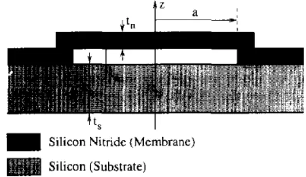
FINITE
ELEMENT MODELINGstructure as depicted i n Fig. 1. The structure is an The cMUT under analysis is considered to have a
m
Silicon Nitride (Membrane) Silicon (Substrate)Fig. 1. Cross-sectional view of c.CIUT structure object of rotation about the z-axis with a being the radius of the active membrane area. The menhrane consists of a silicon nitride layer of thickness t , and the membrane substrate separation is t,. The driving force for the membrane's vibration is the electrostatic attraction force between a metal electrode deposited on the membrane and the silicon substrate. The fol- lowing device dimensions have been used throughout the analyses (Table
I):
The listed dimensions resuksT.4BLE I
DEVICE O M E N S I O N S FOR T H E A N A L Y S E S
Parameter
I
SymbolI
ValueMembrane thickness
I
t ,I
1 . 0 p m Airgap thickness Membrane Radius Substrate thickness 1.0 pm t o t , 500.0pm a 45.0 p min a device whose first order resonance is a t 2.3MHz.
A.s we are primarily concerned with the power that
the membrane couples to the radially outward propa- gating wave mvdes of the substrate, we need to have an absorbing boundary at the radial edges of our model. Levander [4] and Cerjan et ai. [S] have used lossy material boundaries t o absorb waves incident on model boundaries. Later, Berenger's [6] Perfectly Matched Layer (PML) for electromagnetic waves was shown to be applicable t o elastic wave propagation problems by Chew
e t
al.171
and was used in a num- ber of applications [ S ] , 191, 110). I n this study. we use a lossy medium of considerable length to absorb the outward propagating waves. Fig. 2 depicts the finite element model involved in the analysis. The attenua-LOSSY
Lossless
1
# Pressure LoadL
Displacement Constraint Fig. 2. Finite-element model of the chlUT. tion in the lossy part of the model has to be kept smallary of the lossless and lossy regions. On the other to minimize the impedance mismatch at the bound-
hand. the lossy region should provide enough attenu- ation so that incident waves at the model boundary should be well attenuated and the reflected waves at that end should not result in a significant standing wave pattern. This can be achieved by having a very long attenuating region as compared to the largest wavelength.
analyses using ANSYS 5.4 to test the validity of The structure of Fig. 2 is used to run harmonic
our method. The indicated pressure loads are applied together with the displacement constraints. ANSYS
'@SAS IP> 1°C
enables the use of an axisymmetric model, therefore we were able to model the cMUT as the 2-D struc- ture of Fig. 2. As a first check, we look at the par- ticle displacement at the surface of the substrate as a function of radial distance. Displacement is ex- pected t o decay monotonically with
&
[ l l ] . Fig. 3 shows a plot of nodal displacement magnitude as a function of radial distance at a n excitation frequency of 1.5 MHz. The radial distances up to 40nrnl arewave amplitude and
i'"
I i;.*l
,\\1
OO 20 40 60 80 1w 120
Radial Distance (mm)
Fig. 3. Magnitude of nodal displacement on substrate.
there is a good agreement between the magnitude in the lossless region of the model and, as expected.
and the l/& curve shown with the dashed line. For 40 mm< r
<
120 mnr, wave magnitude dies away and: as the plot has reasonable smoothness. there is no significant reflection at either boundary.NORMAL
MODEANALYSIS
bution of particle displacement and stress components The finite element analysis also provides the distri-
along the thickness of the silicon substrate generated
variables t o calculate the total radiation loss to the by the vibrating membrane. One can use these field
gained by identifying the different wave modes using substrate. However, a deeper understanding can be
the 2-D normal mode decomposition [12]. Since the excitation and propagation of the normal modes are well known, the loss mechanisms can be revealed and can he used t o reduce the loss by changing membrane parameters. An arbitrary dist,ribution of particle ve- locity v(z, z ) and associated stress field T(z. z ) along the thickness of the plate can be written as
whereas the So mode is becomes a more important source of loss at higher frequencies. The contrast in the ripple-like structure riding on top of the Lamb wave mode curves suggests that the absorbing bound- ary conditions in the FEA is more satisfactory for the
Ao mode. These results enable us t o derive an equiv- alent circuit model of the membrane with physically based loss terms as described below.
where the orthogonal field distributions vn(t) and T , ( z ) . x are in fact the field distributions of the propa- gating Lamb waves in the free silicon plate. Given the frequency range of interest (1-3.5
MHz)
and a 0.5 mm thick silicon plate, the only propagating modes are the two lowest order antisymmetric ( A , ) and symmetric (S,) Lamb wave modes. The mode amplitude a, can he found by substituting the corresponding orthogo- nal mode expansions for the arbitrary fields in Eq. 1 and 2 in the orthogonality relationa, =
-1
1 0 (-v~(z).T(z)-v(z).T~(z))~xdz. (3) 4 p n n t,P,, is the average power flow of the mode per unit width in the z-direction for a , = 1. To apply this methodology to the circularly symmetric geometry, it is inherently assumed that the calculations are per- formed a t a radius which is sufficiently far away from the membrane.
lossy region, Pt,t can be found by
The total power radiated, hence dissipated by the
0.1
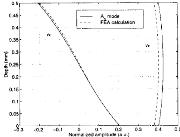
Fig. 4. Particle velocity field distribution of the A o mode and the FEA calculation at 1 MHz (rI=39.G m m ) .
where all stress and velocity values are at a cross sec- tion at T = T I : with T I being inside the lossless part
of the model and close to the boundary of the lossy and lossless regions. The radiated power levels of the Lamb wave modes are then found by substituting the results of the finite element analysis in Eq. 3 and using the relation P, = 2?rrlla,lzP,,.
The modal decomposition results show that the Ao
mode Lamb wave is the dominant source of the radi- ation loss, especialy a t lower frequencies. This can be clearly seen in Fig. 4 where the modal particle veloc- ity field distribution of the Ao mode and the result of the FEA calculation a t 1 MHz are plotted. The anti- symmetric nature of the radiated field is very similar to the A. mode. Radiated power calculation results support this conclusion. The total radiated power loss
as a function of frequency is plotted in Fig. 5 as the solid line. As expected, the radiated power is maxi- mum at the resonance frequency. The ripple-like vari- ations in the total power indicate that there are slight reflections at the boundaries of the
FEA
regions. T h e power radiated by the A0 andS
o
modes are also de- picted in the same figure. It is evident that theAo
mode carries nearly 90% of the total radiated power,
Fig. 5 . Total radiated power calculated by Eq. 4 and the power levels of the A n and So modes.
EQUIVALENT
CIRCUIT
MODEL
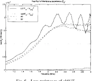
The ideal lossless membrane is modeled asa capac- itor and an inductor in series representing its compli- ance and mass, respectively. Substrate loss can be in- cluded to the model as a series frequency dependent resistor. The value of this resistor can he found by
finding the acoustic impedance Z, of the membrane from FEM results: If the applied pressure on element faces is P , the the total force on the membrane sur- face is F,,, = r a 2
P.
The average velocity of the membrane,VaUg
is given bywhere U ( T ) is the membrane displacement found from the FEM analysis. The acoustic impedance of the membrane is; then, given by Z, = F t O t / V & As
substrate loss, the resistance found by computing the we claim that the real part of Z, accounts for the
power propagating out from the membrane, should be identical to
Re(Z,).
The loss resistance is then given byO.5Pt,~/lVaU,1*,
where PtOt is calculated using Eq. 4.Fig. G. Loss resistance of cMUT
Figure 6 shows that the real part of the membrane impedances computed using the two suggested meth- ods are indeed in agreement. The value of loss resis- tance is about 1/100 of the impedance of air as the
respect, to the radiated power of an air transducer. loading medium. hence. power loss will be -20dB with
each representing the loss due to a different propagat- The loss resistance can be further divided into terms
into the physical loss mechanism. The result of this ing mode in the silicon substrate giving more insight
calculation for the A0 and SO modes are also depicted in Fig. 6.
CONCLUSION
of energy to the silicon wafer. This energy is coupled The main loss mechanism of cMUT is the radiation
to the propagating modes of the silicon wafer at the membrane-substrate junction. Finite element analysis
results combined with the normal mode theory is used to show that the A0 mode is the dominant propagation mode at low frequencies and to derive an equivalent circuit model for a lossy t,ransducer membrane. This analysis enables us to adjust the membrane paratne-
spurious wave modes of the system.
ters to reduce the cross-coupling and loss due to these
REFERENCES
machined electrostatic ultrasomc air transducer," IEEE
M. I. Haller and B. T. Khuri-Yakub. "A surface micro-
Tmns. on Ultrosontcs, Ferroelecfrics and Frequency con^ trol, vol. 43, no. 1, pp. 1-6, January 1996.
face micromachined ultrasound transducers in CMOS tech- P. Eccardt, K. Kaederer, T. Scheiter, and C. Hierold, '"Sur-
nology," in Ultrasomcs Symposrum, San Antonio, Texas, Kovemher 1996, IEEE Illtrasonics. Ferroelectrics, and Fre-
quency Control Socirtv, pp 959-962
I. Ladabaum, X. C. Jin, H. 7. Soh, A. Atalar, and B. T. Khuri-Yakuh, "Surface micromachined capacctive ultra- sonic transducers," I E E E Trans. an Ultrasonics; F w n ~
May 1998.
electrics and Frequency Contml, v01 45, no. 3, pp. 678-690,
sorbing boundary efficiency for fourthorder acoustic W ~ Y C
A. R. Levander, "Use of telegraphy equation t o improve ab- finite difference schemes," B d l . Sezsmzl. Soc. A m , , no. 75, pp. 1847-1852, June 1985.
C. Ceqan, D. Kasloff, R. Kosloff, and M Rrshef. "4 nun re^
flecting boundary condition for discrete awnstic and elastic
wave equations," Geophys%cs,
.
no. 50, pp. 705-708, April 1985.J . P. Berenger, "4 perfectly matched layer for t,he ahsorp-
tion of electromagnetic waves," J . Cornput. Phys , , no.
114, pp. 185-200, 1994.
W . C Chew and Q. H. Liu, " U s q perfectly matched lay-
ers for elartodynamics." in I E E E Antennas Propagation
Society International Symposzvm IEEE Antennas Propa-
gation Society, 1996, pp. 366-369.
F. D. Hastings, J. B. Schneider, and S. L. Broschat, "Ap- plication of the perfectly matched la,yer (PML) absorh- ing boundary condition to elastic wave propagatmn," 3.
A m w t . Soc. Am., , uo. 100, pp. 3061-3069, Kovernher
1996.
Q. Liu and J. TaO, "The perfectly matched la,yer for acous-
tic waves in absorbing media," 3. Acoust. Soc. A m . , no. 102, pp. 2072-2082, October 1997.
[lo] X. Yuan; D. Borup, J. W . Wiskin, hl. Berggren, R. E- dens, and S. Johnson, "Formulation and validation of herenger's PML ahsrxhiog houndarv for the FDTF sirnu- lation of acoustic scattering;" IEEE ?Yam o n Ultrosonzcs;
Fermeiecfncs and Frequency Control, , no. 44, pp. 816-822, July 1997.
1111 G. F. Miller and H. Pursey, "The field and radiation impedance of mechanical radiators on the free surface of
a semi-infinite isotropic sol~d," Proc. Royal Academy, pp.
1121 B. A . Auld. Acousttc F d d d and W a v e s m Solzds, Krieger
521-541, 1953. Publishing C O , 1990.
1028
-
1998 IEEE ULTRASONICS SYMPOSIUM
View publication stats View publication stats