JOURNAL OF SPECTROSCOPY AND DYNAMICS
J. Spectrosc. Dyn. 2012, 2: 3
Probing dynamics of surface structures using X-ray
photoelectron spectroscopy
Hikmet Sezen, Sefik Suzer*
Department of Chemistry, Bilkent University, 06800 Ankara, Turkey
*Author for correspondence: Sefik Suzer, email: [email protected]
Received 2 Apr 2011; Accepted 31 May 2011; Available Online 15 Jun 2011
Abstract
By incorporating laser illumination, and/or by application of electrical square-wave pulses to the sample, X-ray photoelectron spectroscopy is utilized to probe the dynamics of the surface structures in the range of 10-3 to
105 Hz. Different experimental methodologies are introduced, and their applications to investigate certain dynamical properties of two compound semiconductors, CdS and GaN are given. It is shown that dynamics of charging/discharging and surface photovoltage formation and its dissipation, and entanglement of various processes can be investigated by following the voltage shifts recorded in a chemical specific fashion.
Keywords: XPS; Charging/Discharging Dynamics; Surface Photovoltage; Photoconductivity
1. Introduction
X-ray photoelectron spectroscopy, XPS, is a well established analytical tool heavily utilized for extracting chemical composition of surface structures for more than 5 decades, the principle of which is based on analyzing the kinetic energy of the electrons emitted as the result of the monochromatic X-ray exposure. The surface sensitivity, in the range of 6-20 nm is related with the short (2-6 nm) attenuation length of the photoelectrons emitted [1]. However, the technique has so far been used mostly in the static fashion, and only in very limited cases dynamics have been tapped with specially designed equipment and/or with use of synchrotron facilities [2-5]. Laboratory based spectrometers have also been applied to probe the dynamics of slow processes in the orders of minutes to hours only [6-8]. We have recently reported on incorporation of pulsing or modulation techniques while recording XPS data by use of electrical pulses for probing the dynamics of charging/discharging of dielectric and/or surface photovoltage (SPV) development in photoactive materials [9-15]. In addition, the high photon flux of the recent commercial focused monochromatic X-ray sources allows us to acquire data of a narrow spectral region to record in the snap-shot mode in a reasonably fast (sub-second) periods of time, to reveal the transient behavior of a sample, when subjected to external stresses like light illumination [16].
Detailed understanding of the nature and control of the chemical and/or physical changes associated with photoinduced processes
is vital for numerous chemical and biochemical processes as well as their applications in photovoltaics, sensors, etc. One result of the photoinduced changes is the development of an electrical voltage (photovoltage, or surface photovoltage) on different regions of the sample under investigation, which has been extensively investigated using electrical, electrochemical,
spectroscopic, scanning probe microscopic
techniques, etc [17-19]. Use of XPS for probing the so-called surface-photovoltage (SPV), and/or other photoinduced voltage changes, is very appealing, since the observed features are sensitive to small voltage developments down to the orders of 10 meV, where, in the case of core level peaks, chemically specific information can be harvested in addition [20-34]. In XPS analysis of surface structures, the voltage development manifests itself as shifts in the position of the
core level peaks, since the detected
photoelectrons’ kinetic energy is modified by the developed voltage.
In the present contribution, we will focus only on two wide band-gap photoactive semiconductors, CdS and GaN for describing the methodology we have adopted/developed.
2. Experimental
GaN sample was grown on double polished c-plane sapphire by low-pressure MOCVD (AIX 200/4 RF-S). The Mg doped
p-GaN had conductivities of 0.79 S-1.cm-1. Two
different CdS films were used, one was prepared by laser ablation onto a silicon substrate to result
JOURNAL OF SPECTROSCOPY AND DYNAMICS
J. Spectrosc. Dyn. 2012, 2: 3
in ca. 100 nm film, and the other was prepared by casting from slurry acetone solution onto also a silicon substrate. The results were the same for both samples, but only the laser deposited one will be given in this paper.
A Thermo Fisher K-Alpha electron spectrometer with monochromatic AlK X-rays is used for XPS analysis, which is slightly modified for imposing external voltage stress to the sample during data acquisition. The spectrometer is equipped with a low energy flood-gun facility for charge neutralization,
utilizing only electrons or both electrons and Ar+
ions. The sample surfaces were cleaned by
sputtering with medium energy (200 eV) Ar+
ion-gun, till C1s peak fell below detection limit. No annealing of the samples was performed after cleaning.
For probing the charging/discharging properties, the sample is subjected to square wave pulses (SQW) of ±5 or 10 V amplitude
with varying frequencies in the 10-3 to 105 Hz
range using a Stanford Research System DS345 pulse generator. For photoillumination a 100 mW 405 nm laser (CrystaLaser) is employed in the C.W. mode. A shutter connected to a signal generator was used to turn the laser on and off.
3. Results and Discussion
3.1. Static mode and SPV
A typical XPS survey spectrum of CdS and GaN films are shown in Figure 1, recorded in the usual static mode. Detailed analysis of the Cd3d, S2p, Ga2p and Ga3d peaks reveal the composition of the samples to be nearly stoichiometric, with some impurities like O, and C, or the dopant Mg in the case of p-GaN sample, but overlap of some of the Ga Auger peaks prevented recording all of the spectral features like N1s and Si2p (in n-GaN). We also learn that both samples are charged, but can be neutralized by adjusting the current of the flood-gun facility.
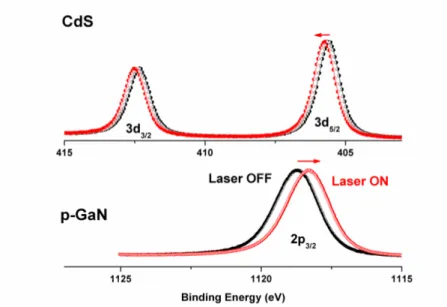
Laser illumination in the C.W. mode causes extra shifts in the positions of XPS peaks as depicted in Figure 2. CdS is one of the well known photoconductive semiconductor and it is frequently employed in solar cell applications
due to its photosensitivity and ideal
photoconductive performance in the visible range [35]. The band gap of CdS is reported as a direct one and at 2.4 eV. Moreover, CdS is naturally an n-type semiconductor due to S vacancies. Accordingly, illumination with 405 nm laser (3.1 eV) leads to reduce the band-Figure 1. Survey Spectra of CdS and p-doped GaN samples, after brief cleaning with Ar+ Ion Gun at low
(200 eV) energies. Besides the main components, in the GaN sample, O impurity and dopant Mg peaks are observable.
JOURNAL OF SPECTROSCOPY AND DYNAMICS
J. Spectrosc. Dyn. 2012, 2: 3
bending and causes a negative shift in the kinetic energy of the photoelectrons, which translates to a positive shift of 0.20 eV in the recorded
binding energy [15]. Similarly, upon
illumination, the wider band-gap and p-doped GaN exhibits a larger (-0.39 eV) shift as also
shown in the same figure [16]. The
impurity/dopant dependence, direction,
magnitude, intensity and wavelength dependence of the SPV give crucial information about the photoactivity of these materials, the discussion of which is beyond the scope of the present paper, since here only the methodology for
recording the dynamics will be emphasized. 3.2. Snap-Shot mode and the SPV
The K-Alpha spectrometer allows us to record with reasonably high signal-to-noise (S/N) ratio of a narrow spectral region with high photoelectric cross section like the Cd3d or Ga2p peaks with 0.1 s intervals. Figure 3 depicts such time-resolved spectra for the two samples while the laser is turned on and off every 50 seconds. As can be gathered from the figure the SPV sets-in a shorter time sets-interval (< 0 1 s) than we are able to measure for both samples, but it gets Figure 2. The Cd35/2-3/2/ and Ga2p3/2 regions recorded as is and under 405 nm Laser illumination.
Figure 3. Variation of the center of the Cd3d5/2 and the Ga2p3/2 peaks recorded with 0.1 s intervals and under
the influence of flood-gun electrons the samples are subjected to the laser illumination turned ON and OFF at 50 s intervals.
JOURNAL OF SPECTROSCOPY AND DYNAMICS
J. Spectrosc. Dyn. 2012, 2: 3
severely screened by the flood-gun electrons for the p-GaN. This indicates that when the flood gun is operative an additional mechanism is triggered just after change of the state of the laser, as a result of interaction between the electrons of the flood gun and the p-GaN sample. This can be explained as follows. The p-GaN develops a certain magnitude of downward band-bending at its surface. This downward band bending at the laser OFF state provides a proper well to capture the flood-gun electrons at or near the conduction band, as schematically shown in the inset of Figure 4 to cause an opposite shift to lower binding energy as expected and measured. When the state of the laser is changed to ON, the
downward band-bending is immediately
flattened and is no longer a well. Hence, the accumulated electrons during the previous state are quickly swept away to the bulk, because now the conduction band of the bulk has many favorable energy levels for the electrons as also shown the inset of the Figure 4. This event is observed as a further shift to a higher binding energy.
Moreover, the time constants of electron accumulation and electron sweeping away from the surface of the p-GaN sample are quite different and are 6.3 and 0.85 s respectively. This difference arises from the different nature of the two mechanisms. The impinging electrons takes
longer to be accommodated, since each accumulated electron contributes to the build-up of the negative sheet charge at the surface, which in turn reduces the rate of accumulation of further negative charge. However, when the laser is turned on, the sweeping of accumulated electrons to the bulk is very effective and quick due to its large volume compared to the surface.
Extension of the method to record the dynamics of surface structures as a result of other kinds of stresses applied, like electrical, chemical, thermal, mechanical, etc. can also be incorporated. In the next section we will demonstrate incorporation of electrical pulses.
3.3. Use of electrical pulses
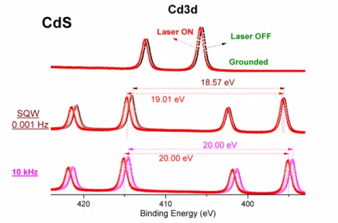
Electrical pulses from a function generator can be used to impose time-dependent changes, as we have recently applied for probing the dynamical nature of the charging/discharging shifts by measuring the positions of the peaks when the sample is under the influence of square wave pulses (SQW) with varying frequencies in
the range of 10-3 to 105 Hz [9-14]. As a typical
application we show in Figure 5 the Cd3d peaks of the CdS sample. As described in our earlier work, for a conducting sample, this procedure results in shifting the position of the peaks by +10.00 and -10.00 eV, respectively, and at the same time enabling the sample to completely Figure 4. The schematic for the formation of the SPV transients in the p-GaN sample, and the exponential
JOURNAL OF SPECTROSCOPY AND DYNAMICS
J. Spectrosc. Dyn. 2012, 2: 3
pull (in the +10 V cycle), or completely repel (in the -10 V cycle) the flood-gun electrons. For the CdS sample, the situation is different due to both charging and photoconductivity related voltage development. The shifts are more pronounced at low frequencies, as the sample finds enough time to charge and discharge at each cycle. The direction and the magnitude of the shifts give information about the resistivity of the samples, and the frequency dependence gives information about its capacitance [15].
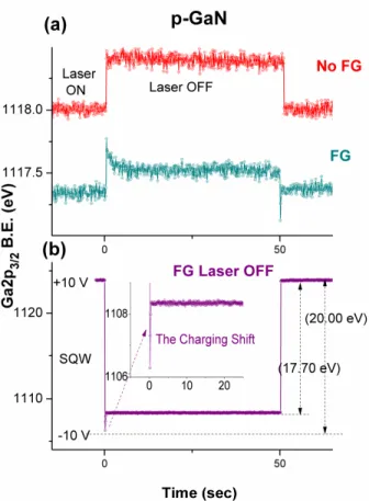
As several different experimental
parameters, like flood-gun electrons,
photoillumination, etc., influence both the magnitude and the dynamics of voltage shifts, we give an example for entangling them from one another in the case of p-GaN in Figure 6.
Whereas the position of the Ga2p3/2 peak is
shifted close to 10.00 eV in the “+” cycle (charging neutralized), the corresponding shift is only 7.70 eV in the “–” cycle, revealing a charging shift of 2.30 eV due to repelling of the low energy electrons, which sets in with a much faster time constant (<< 0.1 s). Comparing these results with the laser excitation (reproduced in the same figure) assures us that the flood-gun electrons do not have any effect on the rise of the SPV transients. However, in the presence of the flood-gun electrons, the transients observed after the OFF-to-ON and the ON-to-OFF transitions are shielded severely, and decay with different time constants, as was discussed above and shown in Figure 4, due to the differences in the nature of the transients.
These findings can now be summarized as follows:
-Charging shifts due to photoemission process are fast and sets in a time scale of less than 0.1 s.
-Surface Photovoltage shifts are also fast and sets-in a time scale of less than 0.1 s.
-The SPV in GaN (and also other p-type systems) are modified and screened by flood-gun electrons, which flattens the SPV. Both of these processes are slow and are in order of seconds.
Now the question arises, whether or not it is possible to probe the mechanism of even faster processes. For fast processes, the general approach is to use more sophisticated pump-probe, lock-in and/or stroboscopic techniques. However, it is also possible to get certain types of information by combining the application of faster SQW electrical pulses together with the snap-shot mode. One possibility is to use the fast SQW pulses and change the frequency
one-at-a-time. In this case, however, obtaining
information spanning a large frequency range is time-consuming and cumbersome. The other possibility is to sweep the frequency at a reasonable rate and ensure that the spectrum obtained has good S/N ratio. Sweeping the frequency can also be done either in linear or logarithmic fashion, and only the latter of which will be shown below. The method requires only the use of a function generator, while recording the XPS data in the snap-shot mode, which is schematically shown in Figure 7.
Figure 5. The Cd3d region of the CdS sample as the sample is grounded and also subjected to SQW
electrical pulses of 10V amplitude and at 0.001 and 10 kHz. Spectra recorded under laser illumination are also included.
JOURNAL OF SPECTROSCOPY AND DYNAMICS
J. Spectrosc. Dyn. 2012, 2: 3
Figure 6. (a) Variation of the center of the Ga2p3/2 peaks recorded with 0.1 s intervals without and under the
influence of flood-gun electrons. (b) The same data while the sample is subjected to SQW electrical pulses with the flood-gun turned on but without the laser.
Figure 7. Schematic diagram of the use the SQW electrical pulses in a continuous but logarithmic sweeping
JOURNAL OF SPECTROSCOPY AND DYNAMICS
J. Spectrosc. Dyn. 2012, 2: 3
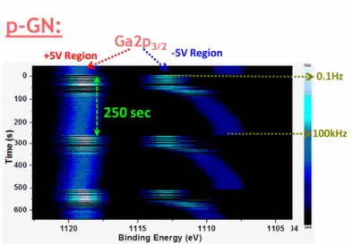
3.4. Sweeping the frequency of the electrical pulses
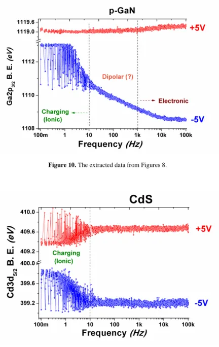
Figure 8 and 9 depict the Ga2p3/2 and
Cd3d5/2-3/2 regions for the two samples, recorded
by sweeping the frequency of the applied SQW pulses with 5 V amplitude from 0.1 to 100 kHz in a logarithmic fashion for a period of 250 seconds. In both cases, only flood-gun is operative, and naturally laser illumination
introduces additional features. For our
measurements, the usable frequency range is dictated by the response characteristic of the entire spectrometer, detectors, cable lengths, resistive, capacitative paths, etc., but can definitely be extended by more careful design.
Even with this limited range, the information which can be harvested is overwhelming.
The p-GaN sample, in the +5 V cycle the sample is neutralized, and in the -5 V cycle the charging sets in at low frequencies, and the sample is continuously less and less charged till frequencies as high as 10 kHz is reached, as shown in a different way in Figure 10. In contrast, in the CdS sample the charging stops around 10 Hz. Although, the analysis of the data is not finalized yet, we can divide the frequency range into 3 regions, roughly corresponding to charging shifts stemming from slow ionic (0.001
to 10 Hz), or dipolar (10 to 103 Hz), and possibly
electronic (>103 Hz) movements. Accordingly
Figure 8. The Ga2p3/2 peak of the p-GaN sample recorded while sweeping the logarithm of the frequency,
spanning the entire 01, H to 100 kHz frequency range in 250 seconds.
Figure 9. The Cd3d peaks of the CdS sample recorded while sweeping the logarithm of the frequency,
JOURNAL OF SPECTROSCOPY AND DYNAMICS
J. Spectrosc. Dyn. 2012, 2: 3
only ionic contribution is observed in the CdS (Figure 11) sample, but all three are operative in the p-GaN sample.
Detailed analysis of the data as well as applications to other systems is obviously the next step, and await incorporation of theoretical models of charge accumulation and separation in these and/or related systems.
4. Conclusions
By incorporating different optical
and/or electrical modulation techniques, XPS spectroscopy, which is conventionally utilized in a static fashion, can also be used for probing the
dynamics of surface structures. Combination of time-resolved XPS, flood-gun electrons (and also ions), and photoillumination give us new ways of investigating surface electronic structure and other surface properties of semiconducting and dielectric materials in a chemically specific fashion.
Acknowledgement
This work was partially supported by TUBA (Turkish Academy of Sciences). We thank Prof. Dr.Atilla Aydinli and Ekmel Ozbay of Bilkent University for providing CdS and GaN samples, respectively.
Figure 10. The extracted data from Figures 8.
JOURNAL OF SPECTROSCOPY AND DYNAMICS
J. Spectrosc. Dyn. 2012, 2: 3
References
1. D. Briggs, M. P. Seah, Practical Surface
Analysis, 2nd (ed.,) Wiley, Chichester, Vol. 1 (1999).
2. M. Marsi, R. Belkhou, C. Grupp, G.
Panaccione, A. Taleb-Ibrahimi, L. Nahon, D. Garzella, D. Nutarelli, E. Renault, R. Roux, M. E. Couprie and M. Billardon, Phys. Rev. B 61 (2000) R5070.
3. M. Marsi, M. E. Couprie, L. Nahon, D.
Garzella, R. Bakker, A. Delboulbe, D. Nutarelli, R. Roux, B. Visentin, C. Grupp,
G. Indlekofer, G. Panaccione, A.
TalebIbrahimi and M. Billardon, Nucl. Instr. Meth. Phys. Res. Section A 393 (1997) 548.
4. M. Marsi, M. E. Couprie, L. Nahon, D.
Garzella, T. Hara, R. Bakker, M. Billardon, A. Delboulbe, G. Indlekofer and A. TalebIbrahimi, Appl. Phys. Lett. 70 (1997) 895.
5. M. Marsi, L. Nahon, M. E. Couprie, D.
Garzella, T. Hara, R. Bakker, M. Billardon, A. Delboulbe, G. Indlekofer and A. Taleb-Ibrahimi, J. Electron. Spectrosc. Relat. Phenom. 94 (1998) 149.
6. K. Hirose, M. Yamawaki, K. Torii, T.
Kawahara, S. Kawashiri, T. Hattori, Appl. Surf. Sci. 237 (2004) 411.
7. K. Hirose, H. Nohira, K. Azuma. and T.
Hattori, Prog. Surf. Sci. 82 (2007) 3.
8. K. Hirose, J. Electron. Spectrosc. Relat.
Phenom. 176 (2010) 46.
9. S. Suzer, A. Dana, J. Phys. Chem. B 110
(2006) 19112.
10. H Sezen, G. Ertas, A. Dana, S. Suzer,
Macromolecules 40 (2007) 4109.
11. S. Suzer, H. Sezen, A. Dana, Anal. Chem.
80 (2008) 3931.
12. S. Suzer, H. Sezen, G. Ertas, A. Dana, J.
Electron. Spectrosc. Relat. Phenom. 176 (2010) 52.
13. H. Sezen, G. Ertas, S. Suzer, J. Electron
Spectrosc. Relat. Phenom. 178-179 (2010) 373.
14. H. Sezen, S. Suzer, J. Vac. Sci. Technol., A
28 (2010) 639.
15. H. Sezen, S. Suzer, Surf. Sci. Lett. 604
(2010) L159.
16. H. Sezen, E. Ozbay, O. Aktas, S. Suzer,
Appl. Phys. Lett. 98 (2011) 111901.
17. L. Kronik and Y. Shapira, Surf. Sci. Rep. 37
(1999) 1.
18. L. Kronik and Y. Shapira, Surf. Interface
Anal. 31 (2001) 954.
19. D. K. Schroder, Meas. Sci. Technol. 12
(2001) R16.
20. J. E. Demuth, B. N. J. Persson, and A. J.
Schell-Sorokin, Phys. Rev. Lett. 51 (1983) 2214.
21. J. E. Demuth, W. J. Thompson, N. J.
DiNardo, and R. Imbihi, Phys. Rev. Lett. 56 (1986) 1408.
22. N. R. Huck, R. S. C. Smart and S. M.
Thurgate, Surf. Sci. 169 (1986) L245.
23. W. Jaegermann, C. Pettenkofer and B. A.
Parkinson, Phys. Rev. B 42 (1990) 7487.
24. A. Schellenberger, R. Schlaff, C.
Pettenkofer, and W. Jaegermann, Phys. Rev. B 42 (1990) 7487.
25. R. Schlaf, A. Klein, C. Pettenkofer, and W.
Jaegermann, Phys. Rev. B 48 (1993) 242.
26. J. H. Yang, Y. Zidon and Y. Shapira, J.
Appl. Phys. 91 (2002) 703.
27. Y. Zidon, J. H. Yang and Y. Shapira, Appl.
Phys. Lett. 81 (2002) 436.
28. R. Buller, H. Cohen, E. Minkin, R.
Popovitz-Biro, E. Lifshitz and M. Lahav, Adv. Funct. Mater. 12 (2002) 713.
29. H. Cohen, R. Maoz and J. Sagiv, Nano Lett.
6 (2006) 2462.
30. H. Cohen, S. K. Sarkar and G. Hodes, J.
Phys. Chem. B 110 (2006) 25508.
31. A. Samokhvalov, R. W. Gurney, M. Lahav,
S. Cohen, H. Cohen and R. Naaman, J. Phys. Chem. B 107 (2003) 4245.
32. S. K. Sarkar, G. Hodes, L. Kronik and H.
Cohen, J. Phys. Chem. C 112 (2008) 6564.
33. H. Cohen, J. Electron. Spectrosc. Relat.
Phenom. 176 (2010) 24.
34. N. J. Halas and J. Bokor, Phys. Rev. Lett. 62
(1989) 1679.
35. D. P. Amalnerkar, Mater. Chem. Phys. 60
(1999) 1.
Cite this article as:
Sefik Suzer et al.: Probing dynamics of surface structures using X-ray photoelectron spectroscopy.