P tm iB i A PIsCSWlSE LINEAR CIRCUIT Sliv.UL^,TOR
USING ASYMPTOTICWAVEFORM EVALUATION.
■ T'.c c 'C r*«·· T T · —. I
<1*^ it »W* W 1»>“ T* i i ^ j 'w ' 4 \i
C r ■ a ^ r **·^
tMI^' · 4M
^ttUm j ta»liU *' Aui!*" .2111;.·,'^^-? 4 ¡TL'i
M· C l ^ -4 * 4 O T ' ^jI uw 'i U v>ai * if % MM iC Q ' t 2 az * N · : í : í : p ' ^ ^>.i •f*'* ·. - ♦ < a>». - a . » -«a .
>t Kmttr · a a l> ··»> 4 UM> 1
,1 <f%, ■ .». , r* -·*·; 3 . ; /* v
a Uli: ti i ' ¿ C C i \ U ' ^ iZ i 0 ^ i k \ d <ra»' i; iM. 4 W L ·
u 4 <» «V I^W 4 4 4
H<w/' il a a <i c«t · « M ^··i· u · « ;.jM4 '« a teM i .
^ ·»«)( a w i' U i '—»' <i H * l/ U 4» · -»*' w *#i.·· ·! i4 a a
^ S S S ^ I S B
T
6 1
·
H B ^ kPLAWE: A PIECEWISE LINEAR CIRCUIT SIMULATOR
USING ASYMPTOTIC WAVEFORM EVALUATION
A DISSERTATION
SUBMITTED TO THE DEPARTMENT OF ELECTRICAL AND ELECTRONICS ENGINEERING AND THE INSTITUTE OF ENGINEERING AND SCIENCE
OF BILKENT UNIVERSITY
IN PARTIAL FULFILLMENT OF THE REQUIREMENTS FOR THE DEGREE OF
DOCTOR OF PHILOSOPHY
By
Satılmış Topçu July 1994 -Sâ.X.(UViı.5:... fdrcf.r.dai Lrτκ
-15·^
I certify that I have read this thesis and that in my opinion it is fully adequate, in scope and in quality, as a dissertation for the degree of Doctor of Philosophy.
' A
Abdullah Atalar, Ph. D. (Supervisor)
I certify that I have read this thesis and that in my opinion it is fully adequate, in scope and in quality, as a dissertation for the degree of Doctor of Philosophy.
Mehmet A. Tan, Ph. D. (Co-supervisor)
I certify that I have read this thesis and that in my opinion it is fully adequate, in scope and in quality, as a dissertation for the degree of Doctor of Philosophy.
I certify that I have read this thesis and that in my opinion it is fully adequate, in scope and in quality, as a dissertation for the degree of Doctor of Philosophy.
(9 A , Omer Morgül, jf/n. D.
t/
I certify that I have read this thesis and that in my opinion it is fully adequate, in scope and in quality, as a dissertation for the degree of Doctor of Philosophy.
I certify that I have read this thesis and that in my opinion it is fully adequate, in scope and in quality, as a dissertation for the degree of Doctor of Philosophy.
Murat A§kar, Ph. D.
Approved for the Institute of Engineering and Science:
Mehmet Baray, Ph.
Abstract
P L A W E : A P IE C E W IS E L IN E A R C IR C U IT S IM U L A T O R U SIN G
A S Y M P T O T I C W A V E F O R M E V A L U A T IO N
Satılmış Topçu
Ph. D. in Electrical and Electronics Engineering
Supervisors:
Prof. Dr. Abdullah Atalar and Assoc. Prof. Dr. M ehm et A . Tan
July 1994
A new circuit simulation program, PLAWE, is developed for the transient analysis of VLSI circuits. PLAWE uses Asymptotic Waveform Evaluation (AW E) technique, which is a new method to analyze linear(ized) circuits, and Piecewise Linear (PW L) approach for DC representation of nonlinear elements.
AWE employs a form of Pade approximation rather than numerical integration techniques to approximate the response of linear(ized) circuits in either the time or the frequency domain. AWE is typically two or three orders of magnitude faster than traditional simulators in analyzing large linear circuits. However, it can handle only linear(ized) circuits, while the transient analysis problem is generally nonlinear due to the presence of nonlinear devices such as diodes, transistors, etc.. We have applied the AWE technique to the transient simulation of nonlinear circuits by using static PWL models for nonlinear elements. But, finding a good static PWL model which fits well to the actual i — v characteristics of a nonlinear device is not an easy task and in addition, static PW L modelling results in low accuracy. Therefore, we have developed a dynamic PW L modeling technique which uses SPICE models for nonlinear elements to enhance
the accuracy of the simulation while preserving the efficiency gain obtained with AWE. Hence, there is no modelling problem and we can adjust the accuracy level by varying some parameters. If the required level of accuracy is increased, more simulation time is needed. Practical examples are given to illustrate the significant improvement in accuracy. For circuits containing especially weakly nonlinear devices, this method is typically at least one order of magnitude faster than HSPICE.
A fast and convergent iteration method for piecewise-linear analysis of nonlinear resistive circuits is presented. Most of the existing algorithms are applicable only to a limited class of circuits. In general, they are either not convergent or too slow for large circuits. The new algorithm presented in this thesis is much more efficient than the existing ones and can be applied to any piecewise-linear circuit. It is based on the piecewise-linear version of the Newton-Raphson algorithm. As opposed to the Newton- Raphson method, the new algorithm is globally convergent from an arbitrary starting point. It is simple to understand and it can be easily programmed. Some numerical examples are given in order to demonstrate the effectiveness of the presented algorithm in terms of the amount of computation.
K e y w o r d s : Circuit simulation, piecewise-linear, DC analysis, transient analysis, AWE, moment matching, Pade approximation.
özet
P L A W E : A S IM T O T S A L E G R I B U L M A Y Ö N T E M İN İ K U L L A N A N
P A R Ç A L I D O Ğ R U S A L B İR D E V R E B E N Z E T İM Y A Z IL IM I
Satılmış
Topçu
Elektrik ve Elektronik Mühendisliği Doktora
Tez Yöneticileri:
Prof. Dr. Abdullah Atalar ve Doç. Dr. Mehmet A . Tan Tem m uz 1994
Çok geniş ölçekte tümleşik (VLSI) devrelerin geçici durum analizinde kullanılmak üzere yeni bir devre benzetim yazılımı, PLAWE, gerçekleştirilmiştir. PLAWE, doğrusal devrelerin analizi için yeni bir yöntem olan asimtotsal eğri bulma (AEB) tekniğini ve doğrusal olmayan elemanların DC gösterimi için parçalı doğrusal (PD) yaklaşımını kullanır.
AEB, doğrusal devrelerin yanıtını zaman veya sıklık alanında bulmak için sayısal tümlev teknikleri yerine bir çeşit Pade yaklaşımını kullanır. AEB, büyük doğrusal devrelerin analizinde geleneksel benzeticilerden tipik olarak yüz veya bin kat daha hızlıdır. Bununla beraber AEB yalnızca doğrusal devreleri kotarabilir. Oysa geçici durum analiz problemi diyot, transistör gibi doğrusal olmayan aygıtların varlığından dolayı genellikle doğrusal değildir. Doğrusal olmayan elemanlar için duruk PD modeller kullanılarak AEB tekniği doğrusal olmayan devrelerin geçici durum benzetiminde uygulanmıştır. Fakat doğrusal olmayan bir aygıtın gerçek i — v karakteristiğine iyi uyan bir duruk PD
model bulmak zordur ve buna ilaveten duruk PD modelleme düşük doğruluk sonucunu verir. Bu yüzden AEB ile elde edilen verimlilik kazancını korumakla beraber benzetim doğruluğunu artırmak için doğrusal olmayan elemanlar yerine SPICE modelleri kullanan bir dinamik PD modelleme tekniği geliştirilmiştir. Böylece modelleme problemi ortadan kaldırılmıştır ve bazı parametreler değiştirilerek doğruluk derecesi ayarlanabilir hale gelmiştir. Eğer istenilen doğruluk derecesi artırılırsa daha çok benzetim zamanına gereksinim duyulmaktadır. Doğruluktaki önemli ilerlemeyi göstermek için pratik örnekler verilmiştir. Özellikle yumuşak huylu doğrusal olmayan aygıtları içeren devreler için, bu yöntem HSPICE ’ tan tipik olarak en az on kat daha hızlıdır.
Doğrusal olmayan dirençli devrelerin parçalı doğrusal analizi için hızlı ve yakınsayan bir dürüm yöntemi sunulmuştur. Varolan algoritmaların çoğunluğu yalnızca sınırlı bir devre sınıfına uygulanabilmektedir. Genel olarak bu algoritmalar ya yakınsamamakta yada büyük devreler için çok yavaş kalmaktadırlar. Bu tezde sunulan yeni algoritma varolan algoritmalardan çok daha verimlidir ve herhangi bir parçalı doğrusal devreye uygulanabilmektedir. Bu algoritma Newton-Raphson algoritmasının parçalı doğrusal sürümü üzerine kurulmuştur. Newton-Raphson yönteminin aksine, bu yeni algoritma herhangi bir noktadan başlayarak her zaman yakınsar. Anlaşılması kolaydır ve basit olarak programlanabilir. Sunulan algoritmanın hesaplama miktarı cinsinden verimliliğini göstermek için bazı sayısal örnekler verilmiştir.
A n a h ta r S özcü k ler: Devre benzetimi, parçalı doğrusal, DC analiz, geçici durum analizi, moment eşleme, Pade yaklaşımı.
Acknowledgment
I would like to express my deepest gratitude to Dr. Abdullah Atalar and Dr. Mehmet A. Tan for their supervisions and encouragements in all steps of the development of this work.
I would like to thank Dr. Erol Sezer, Dr. Murat Aşkar, Dr. Mustafa Akgül and Dr. Ömer Mörgül, the members of my jury, for their motivating and directive comments on my research.
I like to acknowledge the financial support of TÜBİTAK through the Science for Stability Programme for presentation of this work in ISC AS’91.
It is my pleasure to express my thanks to Ogan Ocali for his valuable discussions and comments especially about the popcorn algorithm. I would also like to thank Cemal T. Dikmen and Murat Alaybeyi for their collaboration in writing the core of the program, PLAWE. Thanks to Mustafa N. Yazgan for providing the grafix program to view and print the PLAWE outputs.
A special note of thanks is due to my friends Mustafa Karaman, F. Levent Değertekin, Dilek Çolak, Ayhan Bozkurt and Mustafa Çelik for their moral support and friendship.
Finally, my sincere thanks are due to my family for their continuous moral support throughout my graduate study.
Contents
Abstract [
Özet iîi
Acknowledgment v
Contents vi
List of Figures viii
List of Tables
xi
1 IN T R O D U C T IO N 1
1.1 Simulation T e ch n iq u e s... 2
1.2 Piecewise Linear Modeling of Nonlinear D e v ic e s ... 4
1.3 Formulation of Circuit E q u a tio n s ... 6
2 P IEC EW ISE LINEAR MODELS 7 2.1 Piecewise Linear Representation... 8
2.2 MOS Transistor M o d e l ... 10
2.2.1 4-segment MOS m o d e l ... 10
2.2.2 9-segment MOS m o d e l ... 15
2.3 Bipolar Transistor M o d e l... 18 vi
3 DC ANALYSIS 22 3.1 Katzenelson Algorithm 25 3.2 PWL Newton-Raphson Algorithm ... 26 3.3 The POPCORN A lg o r it h m ... 27 3.4 Numerical E x a m p le s ... 30 3.4.1 Choosing Parameter p ... 31 3.4.2 Choosing Parameter q ... 34
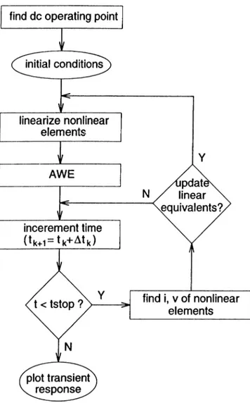
4 A S Y M P T O T IC W AVEFO RM EVALUATION (AW E) 37 5 T R A N S IE N T ANALYSIS W IT H STATIC PW L M ODELING 42 5.1 E x a m p le s ... 45
6 T R A N SIE N T ANALYSIS W IT H D YN AM IC PW L M ODELING 56 6.1 The Method ... 57
6.1.1 Linearization of an MOS Transistor ... 59
6.1.2 Deciding to Update the Linear Equivalents for Nonlinear Elements. 61 6.2 E x a m p le s ... 62 7 CONCLUSION A N D FUTURE W O R K 68 A P P E N D IX 71 Bibliography 73 Vita 82 vii
List of Figures
2.1 The MOS switched resistor model... 8
2.2 The regions of operation for MOS switched resistor model... 9
2.3 The regions of operation for 4-segment nMOS model... 10
2.4 The 4-segment PWL nMOS model: (a) cut-off region (b) forward saturation region (c) linear region (d) reverse saturation region... 11
2.5 Three dimensional plot of nonlinear MOS I-V characteristics... 13
2.6 Three dimensional plot of PWL MOS I-V characteristics... 13
2.7 The equivalent circuit of an MOS transistor... 14
2.8 The CMOS inverter... 14
2.9 Transient response of a CMOS inverter by using SPICE model and 4- segment PWL MOS model {Vt = l.OV, gmin = 10“ ®, for ntype transistor: = 7.25 X 10“ ® and for ptype transistor: gm = 3.5 x 10“ ®)... 15
2.10 The regions of operation for 9-segment MOS model... 16
2.11 Transient response of a CMOS inverter by using SPICE model and 9-segment PWL MOS model {Vdd = 5V, Vt = l.OV, gmin — 10“ ®, for ntype transistor: g^ = 5.56 x 10“ ® and for ptype transistor: gm = 1-94 x 10“ ®). . 17
2.12 The Ebers-Moll model for an npn bipolar transistor... 18
2.13 The regions of operation for a bipolar transistor... 19 2.14 The equivalent circuit of a bipolar transistor... 20 2.15 Bipolar transistor inverter and its response obtained by using SPICE model
and piecewise linear model. 20
2.16 An ECL inverter and its response obtained by using SPICE model and piecewise linear model... 21 3.1 Tunnel diode circuit and the i — v characteristics of the tunnel diodes. . . . 29 3.2 Average number of iterations required for the POPCORN algorithm as a
function of p using q = 0.005 and 4-segment PWL MOSFET model... 31 3.3 The histogram of the number of iterations required in 200 simulation trials
for shl28 circuit using p = 0.2 and q = 0.005... 32
3.4 Average number of iterations required for the POPCORN algorithm as a function of p using q = 0.005 and 9-segment PWL MOSFET model... 33 3.5 Average number of iterations required for the POPCORN algorithm as a
function of q using p = 0.2 and 4-segment PWL MOSFET model... 34 3.6 The results of the POPCORN, PWL Newton-Raphson, and the
Katzenel-son algorithms for the circuit rsync with 500 MOS transistors... 36
3.7 The results of the POPCORN, PWL Newton-Raphson, and the Katzenel-son algorithms for the circuit pgen with 1678 MOS transistors... 36
5.1 Flowchart of the transient analysis with static PWL modeling...43 5.2 Transient analysis results for a large linear RC tree with 9076 elements. . . 46 5.3 A diode transmission gate... 46 5.4 Output voltage waveform for the diode transmission gate... 47 5.5 Transient response of an ECL EX-OR gate... 47
5.6 The input and output waveforms of the CMOS full-adder circuit...48
5.7 Transient simulation results for the address decoder circuit... 49
5.8 Output waveforms of the 5-bit adder circuit... 50
5.9 Output waveforms for the 18-bit adder circuit... 51
5.10 Transient response of a carry-select adder containing 770 MOS transistors. 52 5.11 Transient analysis results for the 128-bit shift register circuit... 53
6.1 Flowchart of the transient analysis with dynamic PWL modeling... 58
6.2 DC equivalent circuit used in transient analysis for an n-type MOSFET. . 60
6.3 Error calculation for a diode equivalent circuit... 61
6.4 Opamp circuit with unity gain feedback... 62
6.5 Schematic of the operational amplifier in transistor level... 63
6.6 Accuracy comparison between our method and SPICE for opamp circuit. . 64
6.7 RC tree driven by a CMOS inverter and the input voltage function...66
6.8 Accuracy vs speed graphs for PLAWE and HSPICE in the second example. 66 6.9 Two CMOS inverters driven by the same inverter... 67
List of Tables
2.1 The piecewise linear equations for 9-segment MOS model...16 2.2 The modes of operation for the bipolar transistor... 19 3.1 Number of iterations taken by PWL Newton-Raphson (NR), POPCORN,
and Katzenelson algorithms to solve various CMOS, ECL and analog bipolar circuits... 35 5.1 Run time comparisons between PLAWE and HSPICE...54
Chapter 1
IN T R O D U C T IO N
There are several steps involved in the design of a very large-scale integrated (VLSI) circuit, which may consist of several hundreds of thousands of components, mainly transistors. The circuit designer first obtains a very high-level functional description of the circuit based on the specifications provided by the user. The synthesis, often called the top-down process, translates this high-level description into various levels including the register level, the transistor level etc. and terminates at the physical mask level. This is followed by the design verification, or the bottom-up process, where a simulation tool is used to predict the performance of the circuit which is compared with the user’s specifications; thus, completing the so-called design loop. If the performance is not satisfactory, certain changes are made and the whole process is then repeated. The total time spent in the design loop is usually referred to as the turn-around time.
The main objective of a VLSI circuit designer is to obtain designs with a turn-around time as low as possible. Computer-aided design (CAD ) tools are used at various steps in the design process to perform tasks which would otherwise take a very long time if they were done by human beings. There is a bottleneck in speeding up the bottorn-up design verification process due to the unavailability of a simulation tool that is capable of accurately predicting the performance of an entire VLSI circuit at a reasonable cost. The accuracy of a simulator is important since otherwise the integrated circuit which is
fabricated and tested might turn out to perform rather unsatisfactorily. For large circuits, the speed of simulation is equally important so that the entire circuit can be simulated in a reasonably small amount of computation time.
There are a variety of circuit simulation tools, with different accuracy and speed, which are used in the circuit analysis and design. The accuracy and speed requirements may vary depending upon the size and type of the circuit. The extensive computations and thus very long simulation times are mainly due to the complex nonlinear characteristics of the devices and due to the large number of iterations for computing the transient response in timing simulation. Almost all the existing circuit simulators use iterative methods (e.g. Newton Raphson) to handle nonlinear characteristics and numerical integration methods (e.g. Forward Euler, Backward Euler, Trapezoidal, etc.) to compute the time domain responses of energy storage elements.
Aspects of stability, convergence and hence completion of the job in a successful manner are all important issues for circuit simulation tools. Moreover, the models of new devices resulting from the emerging technologies must be easily put into a simulator. Otherwise, the simulator may become obsolete in a short time.
By the motivation of these facts, a new circuit simulator, PLAWE (Piecewise Linear Asymptotic Waveform Evaluator) has been developed. PLAWE can solve large circuits containing linear energy storage elements and passive and active linear or nonlinear resistive elements. It uses the Asymptotic Waveform Evaluation (AWE) [1] method and the Piecewise Linear (PW L) approach for DC representation of nonlinear devices.
Chapter 1. INTRODUCTION 2
1.1
Simulation Techniques
Most of the existing simulators for integrated circuits can be classified into two distinct categories, namely, analog simulators and digital simulators. Analog simulators treat an electronic circuit as a continuous dynamical system with the electrical signals such as voltages and currents. Digital simulators, on the other hand, view the circuit as a digital
Chapter 1. INTRODUCTION
network with signals occupying discrete states such as low (0) and high (1). For small
circuit blocks where analog voltage levels are critical in evaluating the circuit performance, analog circuit simulators such as SPICE [2] and ASTAP [3] can be used to predict the performance of the circuit very accurately. These are general purpose simulators in that they can handle almost any type of circuit element such cis resistors, capacitors, inductors, voltage and current sources (independent and controlled), nonlinear devices (transistors, diodes, etc.) and transmission lines. They can also perform many types of analyses such as DC, AC (or small-signal), noise, and transient analyses. However, as the size of the circuit (i.e. number of components) increases, using these simulators is no longer cost- effective. Several decomposition techniques have been used to speed-up their performance and have resulted in the development of a variety of analog simulators such as SLATE [4], MACRO [5], MOTIS [6], MOTIS-C [7], MOTIS-II [8], PREMOS [9], RELAX [10]-[12], SPLICE [13], DIANA [14], SAMSON [15], IDSIM [16], CINNAMON [17], and SPECS [18].
The existing digital simulators can be further divided into Boolean gate-level [19],[20] and switch-level [21]-[26] simulators. In the Boolean gate model a circuit consists of a set of logic gates connected by unidirectional memoryless wires. Information is only stored in the feedback paths of sequential circuits. The Boolean gate model, however, cannot describe some of the new technologies currently used in VLSI circuits, especially circuits with MOS transistors. Because, the MOS circuits consist of bidirectional switching elements connected by bidirectional wires with memory due to the interconnect and device capacitances. The switch-level simulators model an MOS circuit as a set of nodes connected by transistor switches. Each node occupies a discrete number of states 0, 1, or X for the intermediate or unknown state and each switch is either open, closed, or in an intermediate state. Digital simulators, in general, operate at sufficient speeds to test entire VLSI systems, since the circuit behavior is modeled at a logical level rather than a detailed electrical level. However, these simulators do not model the dynamics of the circuits properly and are often useful only in predicting steady-state responses of the circuits. Analog simulators, on the other hand, are fairly accurate in predicting both steady-state and transient responses but they are cost effective only for circuits, with less than a few thousand components.
In many of the VLSI circuits the detail provided by the analog simulators are not lequired for the entire circuit, but only for some critical areas of the circuit. Mixed- mode simulators allow the designer to use a combination of analog simulation and digital simulation, in the same program. These simulators, such as SPLICE [13], DIANA [14], and SAMSON [15], have been observed to realize a one or two order of magnitude reduction in simulation time while still providing a detailed circuit-level analysis where necessary. These simulators, however, work well as long as only small, isolated sections of the circuit need to be simulated as analog circuits. Furthermore, trying to combine analog and digital models in a single program requires rather unsatisfactory approximations at the interfaces. Therefore, unless great care is exercised, a mixed-mode simulator could end up providing the accuracy of a digital simulator at the speed of an analog simulator.
1.2
Piecewise Linear Modeling of Nonlinear
Devices
Chcipter 1. INTRODUCTION 4
Models describe the device behavior to a circuit simulation program. A device model can be used for a variety of different purposes and ideally it would be convenient to have only one model which can serve all the needs. However, different applications impose different requirements on the model. A completely theoretical model based on the fundamental of physics becomes practically intractable. On the other hand, use of a completely empirical model results in a loss of predictive capabilities. A compromise is usually made in developing models for circuit simulation [27].
The nonlinear device models compute the terminal currents of the device in terms o f the terminal voltages. These terminal currents should be continuous functions of the terminal voltages for convergence. Sometimes, it is easier to divide the operating range o f the device into different regions so that the model equations can be conveniently formulated. Since different equations are used for each region of operation, it is important to make sure that the terminal currents are continuous across the region boundaries. In
Chapter 1. INTRODUCTION
DC analysis, it is possible to encounter wide variations in the terminal voltages. Therefore, it is important to consider the entire voltage range while formulating the model equations even though the device will not encounter these voltages in practical circuits.
During model development, it is important to keep the following paradox in mind. More complex models can potentially represent the device characteristics
more accurately. But, it is more difficult to extract all the model parameters for such complex models in a computationally efficient manner. In addition, if the model parameters are not specified properly, the device characteristics will not be reproduced accurately.
In PLAWE, piecewise linear models are used to characterize the nonlinear devices since one of the major goals is to finish the simulation in a reasonably short time. The main reason behind the choice of PWL approximation is that it results in a set of linear equations and hence the iterative solutions of nonlinear equations are avoided. So, the time complexity is decreased and the convergence in DC analysis is guaranteed. Since AWE can be applied only to linear(ized) circuits, the PWL approach can make usage of the AWE technique in the simulation of nonlinear circuits. The user can create his/her own device models for nonlinear elements. Hence, the PWL approximation enables the user to determine the trade-off between the speed and accuracy of the simulation.
PLAWE employs PW L models which can be built at various levels of accuracy to describe two and three terminal nonlinear devices. A two-terminal nonlinear device is represented by a linear equation in terms of its branch voltage and current as
av + bi c = 0
in every region of the (u, i) plane. Similarly, a three-terminal nonlinear device model consists of a set of regions in the (ui, ^2, ¿1, ¿2) space. Every region is represented in terms of two linear terminal equations of the form
T 02*^2 + bikil + i>2A;*2 + Cjfc = 0, k = 1,2
It should be noted that the accuracy of the PWL model for a nonlinear device depends on the number of regions into which the terminal equations are linearized. However, as
the number of regions increases, the complexity of the analysis may increase dramatically. Nevertheless, it is observed that, with the inclusion of constant grounded capacitances, models o f diodes and transistors with only a few segments (2 segments for diodes and 4 segments for M OSFET’s) yield quite good results for timing analysis.
1.3
Formulation of Circuit Equations
Chapter 1. INTRODUCTION 6
In PLAWE, Sparse Tableau Analysis (STA) method [28] is used to formulate the circuit equations. In STA method, with nonlinear devices replaced by linear equivalents, the circuit is described with a large and sparse matrix equation, involving the Kirchoff’s Current Law (KCL), Kirchoif’s Voltage Law (KVL) and the Branch Constitutive Equations (BCE). A KCL equation is written in terms of branch currents for each node. A KVL equation relating a branch voltage to its node voltages is written for each branch. Finally, a branch constitutive equation is written for each branch in terms of its branch voltage and current. Collectively, these equations may be written as follows:
/ 0 0 A G, Ri or in compact form 0 0 ' Vb '
0
0
Ib0
—0
. . Wi w KVL KCL BCE (1.1) Ti X + y t -- y(
1
.
2
)
where Vi, Ib, and are branch voltages, branch currents, and node voltages, respectively. The vectors yi and y denote the equivalent sources due to linearization of nonlinear elements and the independent sources, respectively. The subscript / denotes the linear region in which the circuit operates. The size of STA matrix is (26 + n) where 6 is the number of branches and n is the number of ungrounded nodes in the circuit.
Chapter 2
PIECEW ISE LIN EAR MODELS
A simulator that utilizes piecewise linear models can achieve simulations of arbitrary accuracy because piecewise linear models can be made to conform to nonlinear device characteristics with arbitrary precision by simply adding regions of linearity. However, as pointed out in the preceding chapter, complex models degrade the efficiency of the simulator. Simpler models yield more efficient simulations, and there are strong incentives to use models that are as simple as possible.
Several restrictions can be placed upon the piecewise linear models in order to preserve the efficiency of simulation. First, the number of piecewise linear regions must be small. This is necessary to keep the principle advantage of the AWE technique: the ability to take large time steps. Secondly, only linear capacitors are allowed in the models. Nonlinear capacitors must be modeled using equivalent linear capacitors. Although it may be possible to approximate nonlinear capacitors with piecewise linear capacitors, this was not explored. Finally, the DC coupling from the gate (base) to the source and drain (emitter and collector) for an MOS (bipolar) transistor can be restricted to be unidirectional. This facilitates circuit partitioning which is not explored in this thesis. After a brief discussion of the representation of piecewise linear models, this chapter describes simple MOS and bipolar models and simulations are given to demonstrate the capabilities of these models.
Chapter 2. PIECEWISE LINEAR MODELS
2.1
Piecewise Linear Representation
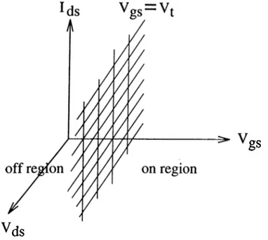
A piecewise linear device is represented by a collection of linear circuits, each of which represents the linearized behavior of the device for a particular region of operation. Each region of operation is a polytope [29],[30] described by a conjunction of linear inequalities in terms of the device’s terminal voltages. Each inequality represents a hyperplane boundary. For example, a description of the MOS switched resistor model which is just a particular piecewise linear model is shown in Fig. 2.1 and Fig. 2.2. The electrical behavior of the device in each of its two regions is modeled by the circuits in Fig. 2.1 (a) and (b). In Fig. 2.2, the region to the right of the plane labeled = Vt is the polytope corresponding to the on region while the region to the left of the plane is the polytope corresponding to the off region. More general models may have circuits consisting of interconnections of linear circuit elements. Additionally, they may have more than two regions of linearity.
g
Vd
Vd
Vd
I 1 1 L > V g -n 1 1Vs
Vs
Vs
(a) on: Vgg > (b) off: Vgs
F igu re 2.1: The MOS switched resistor model.
In general, a device may have n terminals. Without loss of generality, we can concentrate on the voltage-controlled devices. Consider the n dimensional space defined by the voltages at those terminals: {ui, U2, . . . , Un}· Then the set of points whose coordinates satisfy a given linear equation in those voltages:
ÜQ -f aiVi -|- 02^2 ■!■···+ On^n — 0 (2 .1) defines a hyperplane in the n dimensional space. The hyperplane is simply the multidimensional generalization of the familiar three dimensional plane. Like planes.
Chapter 2. PIECEWISE LINEAR MODELS
gs
Vds
Figure 2.2: The regions of operation for MOS switched resistor model.
hyperplanes partition space. Points that lie on one side of the hyperplane have coordinates that satisfy the inequality:
Oo + aiVi + tt2V2 + --- h OnVn < 0
while points on the opposite side satisfy:
ao + oiVi + a2V2 H--- l· OnV„ > 0
(2.2)
(2.3)
The polytope is the multidimensional generalization of the polyhedron. While a polyhedron is a region bounded by planes in three dimensional space, a polytope is a region bounded by hyperplanes in n dimensional space. Equations 2.2 and 2.3 suggest that a poly tope can be specified by a conjunction of linear inequalities:
O o " t " O i U i + 0 2 ^ 2 T ■ ' ■ T ^ 0
bo + biVi + 62U2 + ---- l· bnVn > 0 Co + CiVi + C2V2 + ---- l· CnVn > 0
: (2.4)
2.2
M OS Transistor Model
Chapter 2. PIECEWISE LINEAR MODELS 10
2.2.1
4-segment M O S model
The regions of operations for the 4-segment model are plotted in Fig. 2.3. This model has 4 regions of operation corresponding to cut-off, forward saturation, linear, and reverse saturation states of an MOS transistor. Although there are four regions, any given region is bounded by only two hyperplanes. This is particularly important as far as the efficiency is concerned because the effort required to detect whether a piecewise linear device changes region is proportional to the number of boundaries of the current region.
Vc
gs
F igu re 2,3: The regions of operation for 4-segment nMOS model
The resulting 4-segment MOS model is depicted in Fig. 2.4. In the cut-off region the MOS transistor is replaced by an open circuit. Hence, the drain-to-source current in this region is zero. In the forward saturation region the MOS transistor is modeled by a linear voltage controlled current source. The transconductance is set by the parameter
gm·, while the gate-to-source voltage for which the current source delivers zero current is
Vt. In the linear region, which contains both the forward linear and reverse linear regions, the MOS transistor is modeled by a conductance, g¿s. In the reverse saturation region
Chapter 2. PIECEWISE LINEAR MODELS 11 g Vd
Vgs < V t
V g s - V ds < V t(a)
Vd ^ g —Vgs > Vt
Vgs “ Vds < V{
(b)
g Vdg ds
Vgs > Vt
V g s - V d s > V t (C) Vd V g — ( i ) i = ^ ( V g d - v , )v<
(d)
Vgs < Vt
Vgs- V d s > V (
F ig u re 2.4: The 4-segment PWL nMOS model: (a) cut-ofF region (b) forward saturation region (c) linear region (d) reverse saturation region.
Chapter 2. PIECEWISE LINEAR MODELS 12
the MOS transistor is modeled by a linear voltage controlled current source. The current source is controlled by the gate-to-drain voltage Vg¿ since the drain-to-source voltage, is negative in this region. The inequalities in Fig. 2.4 define the hyperplane boundaries for each region of operation. Consequently, the piecewise linear equations describing the behavior o f an nMOS device in the four regions are:
Ida — ^ (2.5)
0 Cut-off: < v; , 1/^, - Kd, < Vt
9m{Vgs - Vt) Forward saturation: ^ < Vg¡ — Vt < Vds
9dsVds Linear: > V , Vgs - Vds > V
—9m{Vgd — Vt) Reverse saturation: Vds < Vgs — Vt
The same MOS device equations also apply to the pMOS device. The only difference is the change in the sign associated with the voltages and drain-to-source current. It is seen from Eqn. (2.5) that on the boundary between the forward saturation and linear regions (i.e., Vds — Vgs - 14), the drain-to-source current is hs = 9mVds = 9dsVds·
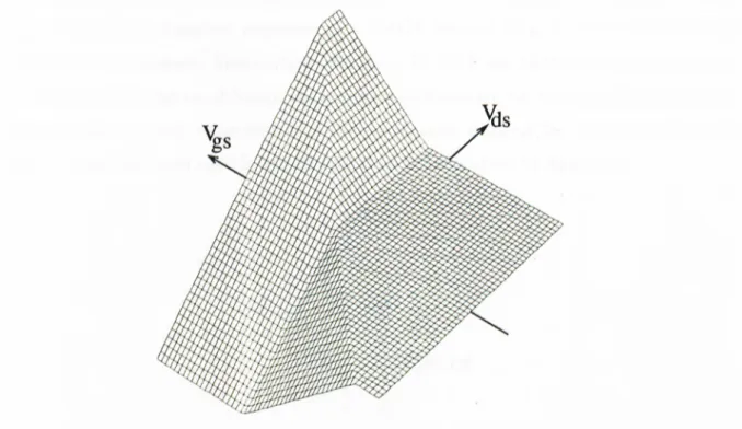
Therefore, the conductance gds must be chosen to be equal to the transconductance gm for preserving the continuity of Ids- In order to illustrate the ability of 4-segment piecewise linear model to match the nonlinear I-V characteristics of an MOS transistor, the three dimensional visualizations of the nonlinear and piecewise linear MOS characteristics are given in Fig. 2.5 and in Fig. 2.6, respectively. In these figures, the z-axis which is not depicted, represents the drain-to-source current {Ids) of the transistor.
In a VLSI circuit every transistor may have a different physical geometry, i.e. their channel widths (IT) and channel lengths {L) may be different from each other. We know that the channel current is dependent on the device geometry. This means that the width and length of the channel must be taken into account while calculating the drain-to-source current. For this purpose, the value of Ids calculated from (2.5) is multiplied by the { Wj L)
ratio, which depends on the actual geometry of the device.
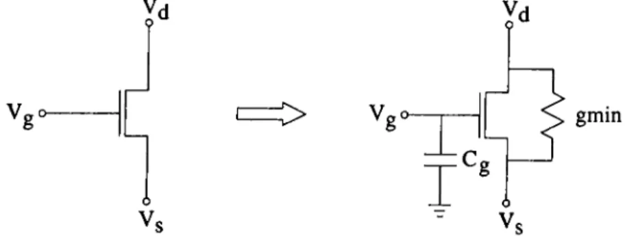
In addition to the linear circuit elements in the 4-segment model given in the Fig. 2.4, a very small conductance, gmin, is placed in parallel with the drain to source nodes of the MOS device. This conductance is used to eliminate the potential problems which may occur due to the open-circuit equivalent of off transistors (Fig. 2.4 (a)). It also enhances
Chapter 2. PIECEWISE LINEAR MODELS 13
Figure 2.5: Three dimensional plot of nonlinear MOS I-V characteristics.
Chapter 2. PIECEWISE LINEAR MODELS 14 V„o-Ó Vc C> yd = ^ C c gmm
F igu re 2.7: The equivalent circuit of an MOS transistor.
the DC convergence properties of the circuit. The nonlinear and/or floating capacitances o f the MOS device is modeled by using linear grounded capacitors. It may be possible to include grounded capacitors from the drain, gate, and source nodes to the ground. The 4-segment MOS model includes one linear capacitor, Cj, from gate node to ground. This approximation has been effective for most MOS circuits because the majority of the capacitances is connected to ground. Therefore, the MOS transistors are replaced by an equivalent circuit shown in the Fig. 2.7.
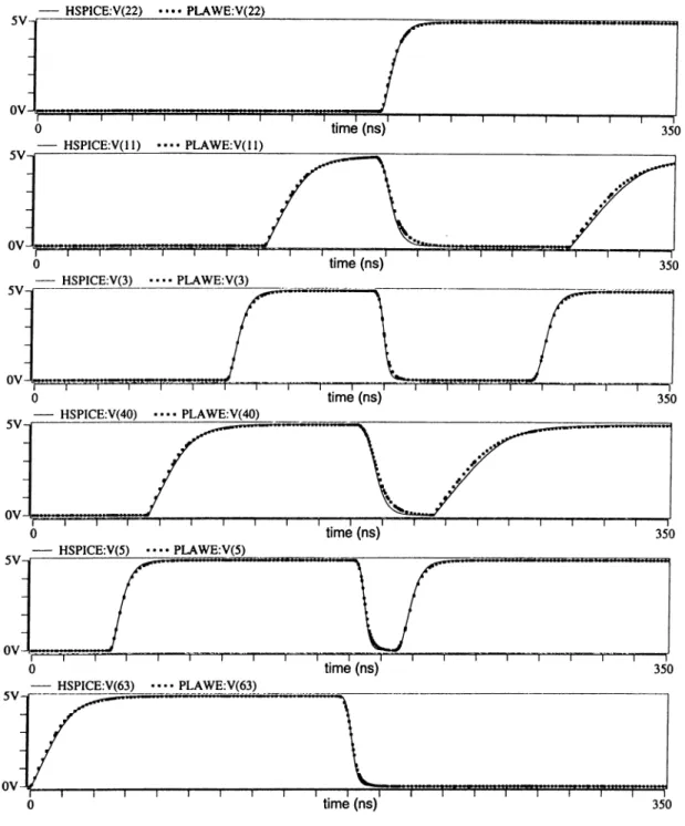
In order to demonstrate the ability of 4-segment model to duplicate the nonlinear MOS characteristics, the transient responses of a CMOS inverter (Fig. 2.8) obtained by using SPICE and our piecewise linear circuit simulator PLAWE are plotted in the Fig. 2.9. As it is seen from this figure, although the output waveforms are not identical, the 4-segment model provides a good measurement of the propagation delay of the inverter to the 50% point. The MOS model used in the SPICE simulation is given in Appendix.
?5V
m out
:CL=0.Ipf
Chapter 2. PIECEWISE LINEAR MODELS 15
0
5
10
Time (ns)
15
20
F ig u re 2.9: Transient response of a CMOS inverter by using SPICE model and 4-segment PW L MOS model {Vt = l.OV, gmin = 10"®, for ntype transistor: — 7.25 x 10"® and for ptype transistor: gm = 3.5 x 10"®).
2.2.2
9-segment M O S model
As stated previously, accuracy of the simulation can be increased arbitrarily by simply adding regions of linearity to the piecewise linear models of nonlinear devices. Therefore, we extracted the 9-segment PWL MOS model which matches the nonlinear I-V characteristics of MOS transistor better than the 4-segment model. The regions of operations for the 9-segment model are plotted in Fig. 2.10. Note that there are 4 regions for the linear state, 2 regions each for the forward and reverse saturation states, and 1 region for the cut-off state of an MOS transistor. The piecewise linear equations describing the behavior of an nMOS device in the 9-segment MOS model are given in the Table 2.1.
Similar to the 4-segment model, the MOS transistor is replaced by the equivalent circuit shown in the Fig. 2.7 and the current {Id,) calculated from the Table 2.1 is multiplied by the { W ¡ L) ratio to include the effect of the device geometry.
^ g sA
Chapter 2. PIECEWISE LINEAR MODELS
©
Forward
saturation
'2 16Cut-off
©
(Vdd+V,)/2i ® >
% (Vdd+Vt)/2Figure 2.10: The regions of operation for 9-segment MOS model.
R egion Equation Boundaries
C u t - o f f Region 1 /d, = 0 F,. < Vt Vgd < K F o r w a r d s a t u r a t i o n Region 2 ^ds “ 9m {Y gs V , < V „ < (Vm + V , ) / 2 K i < V,
Region 3 Ids = Omi-AVgs — Vdd — 2Vt) Vgs > (Vdd + V t ) / 2 Vgd < K
L i n e a r Region 4 Ids — 9m {Y gs K < Vg, < (Vdd + V t ) / 2 Vt < Vgd < (Vdd + V t ) ! 2
Region 5 Ids — QmiYgs ~ ^^gd + ^dd + K) Vt < Vgs < (Vdd + V t ) l 2 Vgd > (Vdd + V t ) l 2
Region 6 Ids = d m i^V gs — Vgd — Vdd — V t) Vgs > (Vdd + V t ) ! 2 Vt < Vgd < (Vdd + V t ) ! 2 Region 7 Ids ~ ^ 9 m {^ g s Vgs > (Vdd + V t ) ! 2 Vgd > (Vdd + V t ) ! 2 R e v e r s e s a t u r a t i o n Region 8 Ids ^ 9m {^ g d K . < V, V , < < ( Vm + V , ) / 2 Region 9 Ids = - 9 m { 3 V g d - Vdd - 2 V t ) Vgs < Vt Vgd > (Vdd + V t ) / 2
Chapter 2. PIECEWISE LINEAR MODELS 17
In order to demonstrate the performance of the 9-segment model, the transient responses of a CMOS inverter (Fig. 2.8) obtained by using the SPICE model and the piecewise linear model are plotted in Fig. 2.11. The SPICE MOS model used for this example is given in Appendix. It is seen from Fig. 2.11 that the output waveform produced by the piecewise linear simulator is very close to that produced by SPICE. In addition to this, the 9-segment model improves the accuracy of the simulation significantly compared to the 4-segment model.
"o
0
0
10
Time (ns)
15
20
F ig u re 2.1 1: Transient response of a CMOS inverter by using SPICE model and 9- segment PW L MOS model (Vdd = 5V, = l.OV, grain = 10“ ®, for ntype transistor:
2.3
Bipolar Transistor Model
The piecewise linear bipolar transistor model is extracted using the well-known Ebers- Moll model [31] which is shown in the Fig. 2.12. The terminal currents Is and Ic can be expressed in terms of the diode currents as
Ie = Ide — ocrIdc
Ic = oipIcE — Idc (2.6)
The terminal current Ip can be obtained by Kirchoff’s current law as Ib = Ie — Ic·
Chapter 2. PIECEWISE LINEAR MODELS 18
I Vbc
*'BE
F igu re 2.1 2: The Ebers-Moll model for an npn bipolar transistor.
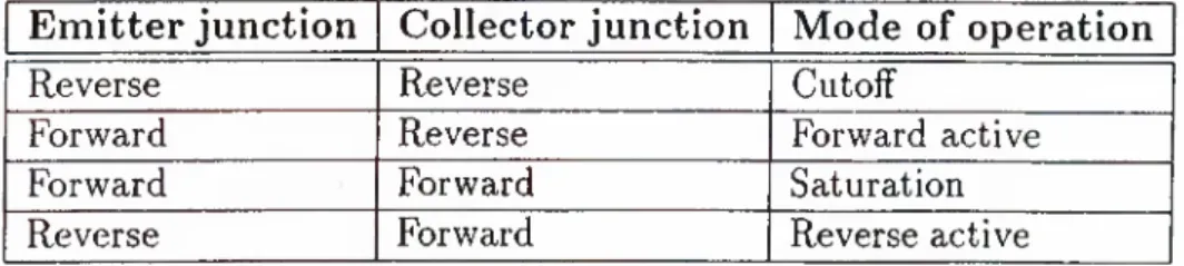
Bipolar transistor has four possible modes of operation listed in the Table 2.2 as a function of the bias that is applied to the emitter and collector junctions. Therefore, by using a simple on/off model for the diodes in the Fig. 2.12, we can divide the operating region of a bipolar transistor into four linear regions as shown in the Fig. 2.13. Then, the piecewise linear equations for the diode currents Ide and Idc can be written as
Ide = 9ejVßE + hoj
Idc = gcjVßc + hoj (2.7)
Chapter 2. PIECEWISE LINEAR MODELS 19
E m itte r ju n c tio n C o lle c to r ju n c tio n M o d e o f o p e ra tio n
Reverse Reverse Cutoff
Forward Reverse Forward active
Forward Forward Saturation
Reverse Forward Reverse active
T a b le 2.2: The modes of operation for the bipolar transistor.
Now let us combine Eqns. (2.6) and (2.7), and we have the piecewise linear equations for the terminal currents Ie and
Ic-Ie = 9ej Ув е — ocr 9cj У в е + { h o j — ocr Icoj)
Ic = 9ej Уве - 9cj Уве + ( «f hoj — hoj) for j —1,2, . . . (2.8)
Note that if each diode in the Ebers-Moll model is modeled with n piecewise linear segments, then our bipolar model will have regions of operation. So, we can improve the accuracy of bipolar model by simply adding linear segments into the diode models.
We model the nonlinear floating capacitances of the bipolar device using equivalent linear grounded capacitors. For this purpose, we include a linear capacitor from base-to-ground in the bipolar model as shown in the Fig. 2.14. In addition, a very small
V pBC
Í Reverse
Chapter 2. PIECEWISE LINEAR MODELS 20
conductance ginin is placed in parallel with both the base-emitter and base-collector junctions (Fig. 2.14).
Bo-gmin i >
Bo-gmin
F igu re 2.14: The equivalent circuit of a bipolar transistor.
The Fig. 2.15 depicts a bipolar inverter and compares the response of the circuit using piecewise linear and SPICE models. The match between waveforms is quite good especially considering the simplicity of the piecewise linear model.
F ig u re 2.15: Bipolar transistor inverter and its response obtained by using SPICE model and piecewise linear model.
Chapter 2. PIECEWISE LINEAR MODELS 21
An ECL inverter [31] and its transient response obtained by using piecewise linear and SPICE models are given in the Fig. 2.16. The inverting and noninverting outputs of the ECL inverter are loaded with Cl = O.lpf. As it is seen from Fig. 2.16, output of the piecewise linear simulator fits very well with the SPICE outputs. The SPICE BJT model used for the bjt inverter and ECL inverter examples is given in Appendix.
F igu re 2.16: An ECL inverter and its response obtained by using SPICE model and piecewise linear model.
Chapter 3
D C ANALYSIS
Finding the “operating point” or “DC solution” of a circuit is usually the first step in the analysis of nonlinear circuits. It is the basis for DC sweep and usually provides the initial conditions for transient analysis and a DC operating point for ac analysis. DC analysis is important not only from a circuit theoretic point of view, but even more so from a computational point of view. Indeed, an essential part of most nonlinear transient analysis computer programs for solving dynamic nonlinear networks is a DC analysis subprogram. In the transient analysis, the DC network, obtained by replacing the capacitors by equivalent voltage sources and the inductors by equivalent current sources, usually possesses a unique solution. In other situations, a DC resistive nonlinear network obtained by open-circuiting all capacitors and short-circuiting all inductors may actually possess several distinct solutions. DC analysis involves determining node voltages for given values of DC sources and it is equivalent to the solution of nonlinear algebraic systems o f equations. A well-known technique for solving systems of nonlinear equations is the Newton-Raphson iteration scheme. For well-behaved problems, this method converges rapidly. However, it may, under certain circumstances, diverge or oscillate about a solution.
In many cases, the equations describing the nonlinearities are not known in functional form and only tables of measured values are given. In other cases, the functions may
Chapters. DC ANALYSIS 23
be known but are very complicated and it is convenient to replace the nonlinearities by piecewise linear equations to take advantage of the linearity. PLAWE uses piecewise linear models to describe the nonlinear devices. For DC nonlinear circuit simulation, PW L analysis is attractive because it can provide important features such as convergence in DC analysis, computational efficiency, and a clearly defined accuracy/speed trade-off.
A nonlinear resistive circuit can be described by
g( x) = y (3.1)
where g(·) is a continuous nonlinear mapping from into itself, a; is a point in J?" and represents a set of chosen circuit variables and y is an arbitrary point in i l " which represents the inputs to the circuit. Various methods are available and many computer programs exist for the solution of (3.1). These methods can be classified into two major groups. One is based on an iterative algorithm which is applied directly to the nonlinear circuit equations. The well-known method in this group is the Newton-Raphson method [32]-[35]. The second group is based on the technique of piecewise-linear (PW L) approximation and PWL analysis which hcis been investigated by many researchers due to its computational efficiency [36]-[48].
In the PWL analysis of nonlinear circuits, the operating region of every nonlinear element is divided into a finite number of segments, and the nonlinear mapping fli(·) is approximated by a continuous PWL mapping / ( · ) , that is linear on each segment. As a result of this approximation, the space i l ” is divided into .V linear regions bounded by hyperplanes. In general, is a very large number. Then, the system of PWL equations
f { x ) = y
can be expressed by the following set of linear simultaneous equations
Ai X + wi = y , for <7/, / = 1.2,
(3.2)
(3.3)
where At is a constant n x n matrix (called Jacobian matrix for convenience) and Wi is a constant n-vector. They characterize the circuit in linear region at. Several methods
Chapters. DC ANALYSIS 24
have been developed for solving (3.3). Some of the existing methods can only be applied to a restricted class of PWL resistive circuits with a unique solution or with topological limitations [40]-[44]. These restrictions are usually imposed in order to obtain a more efficient algorithm. To find all solutions of (3.2), one may solve n linear simultaneous equations in (3.3) for each of N linear regions to find and decide whether Xi lies within the considered linear region, <t/. If Xi lies within <7/, it is a valid solution. This method is conceptually simple and finds all existing solutions, but it is computationally complex. Hence, the major issue in PWL analysis is the reduction of complexity. Recently, a number of authors have proposed various methods [36]-[39] to decrease the number of linear regions, N, by a sign test. This test gives a necessary and sufficient condition on the existence of a solution in a given linear region. One of these methods [36] requires more than 0{N'n?) multiplications. Moreover, the sign test is not a simple procedure. A more efficient method is proposed in [37]. Nishi [38] has proposed a method in which the number o f multiplications required to find all solutions of (3.3) is 0{N n ). Although the method developed in [39] seems to be the best, it is computationally impractical for large PW L circuits containing several thousands of elements. For instance, if the circuit contains 1000 MOS transistors each of which is modeled with 4 segments, then there are 4^°°° (approximately 10®°°) linear regions. If the sign test requires at least one multiplication for each linear region, it will take much more than billions of years on today’s supercomputers to find the solutions by using these methods.
In this chapter, we present a new algorithm [49], which we call ■popcorn., shown to be more efficient than the existing algorithms of the same generality. This algorithm is globally convergent for a general class of PWL resistive circuits with no restrictions. It is simple and can be easily programmed. In Section 3.1, the method of PWL analysis o f nonlinear resistive circuits is reviewed and the Katzenelson algorithm is described. In Section 3.2, the piecewise linear version of the Newton-Raphson algorithm is explained. The POPCORN algorithm, which is particularly geared toward the analysis of large PWL circuits, is presented in Section 3.3. Some numerical examples are given in Section 3.4 to illustrate the effectiveness of the POPCORN algorithm compared to Katzenelson and PW L Newton-Raphson algorithms.
Chapters. DC ANALYSIS 25
3.1
Katzenelson Algorithm
In PVVL analysis, the well-known technique due to Katzenelson [40] has been originally applied to the circuits with two-terminal elements which are strictly monotonic. The PW L approach was further extended to include the resistive circuits of much broader class [43]-[48j. In particular, Fujisawa and Kuh [44] have shown that the Katzenelson’s algorithm can be applied to (3.2) and it always converges to a solution as long as the equation has a unique solution. Fujisawa, Kuh, and Ohtsuki [45] have shown that if all the Jacobian matrix determinants detA /, I = 1,2, in (3.3) have the same sign, then there exists at least one solution to the equation f ( x ) — y and the algorithm also converges. This property is referred to as the sign condition. This restriction of the sign condition was later removed in the generalized Katzenelson’s method [46],[48].
Previously, PL AWE was using the Katzenelson algorithm to find the operating segments of nonlinear elements and compute the DC solution. This algorithm computes the solution for a given input in an iterative manner starting from a valid solution for an arbitrary input. A brief description of the Katzenelson Algorithm is as follows [40],[43]. To determine the solution, we first choose an initial guess Xq in, say, linear region ctq. We rewrite the Eqn. (3.3) here for convenience
AqX Wq = y , for <7o. (3.4)
Substituting Xq into (3.4), we obtain
AqXq -f m>o = yo (3-5)
where yg is called the initial source vector. Combining (3.4) and (3.5), we have
X = Xo + A o \ y - yo). (3.6)
If it happens that the calculated x in (3.6) lies within the linear region ao, then x is the correct solution. Usually, it is not, and we proceed with the following iteration. To determine the next starting point, we connect Xq and the calculated a; by a straight line.
Chapters. DC ANALYSIS 26
The next starting point, Xi is the intersection of this straight line and the boundary of linear region <to where we started. Thus
®i = ®o + Ao>loTy -
Vo) (3.7) where Aq is a scalar parameter in the range of 0 < Aq < 1. Katzenelson has proposed that Ao may be selected such that the operating point of only one nonlinear element goes to the boundary of its present segment. Assuming that Xi lies on the common boundaries o f linear regions ao and ai, the piecewise linear model of the circuit corresponding to the linear region a^ must be used in the next iteration. The point X2 is determined in asimilar manner by evaluating x from (3.5) and (3.6) but using Xi, A\ and Wi instead of «0, Ao and Wo, respectively. Note that in calculating X2 from the new starting point Xi,
the trajectory always move away from linear region ao. This is because of the fact that for circuits with a unique solution the determinant of the Jacobian matrix does not change sign from one linear region to another. Thus, every linear region in the circuit variable space is entered at most once, and this guarantees the convergence of the iteration process for circuits with a unique solution.
This process continues until a solution is reached. The number of required iterations depends heavily on the distance of the starting point from the correct solution. However, finding a good initial guess is a rather difficult task, particularly for large-sized circuits. Furthermore, the Katzenelson algorithm has no guarantee of convergence for circuits with multiple solutions such as flip-flops. In fact, Katzenelson has proved that his algorithm is convergent only for the networks which consist of 2-terminal elements [40].
3.2
P W L Newton-Raphson Algorithm
Newton-Raphson technique is a well-known method for the computer-aided analysis of general nonlinear (i.e., not necessarily PWL) resistive circuits. It is widely used for solving the systems of differentiable nonlinear simultaneous equations. There exists also a piecewise linear version of the Newton-Raphson method [33]. A brief description of the
Chapters. DC ANALYSIS 27
PWL Newton-Raphson method may be presented as follows. To begin with, an initial linear region, say ctq, is chosen, in which the circuit is characterized by the equation
Solving (3.8) for X , we obtain
Aqx + Wo = y.
= ^0 (y - « ’o).
(3.8)
(3.9) Observe that the value of Xi depends on the initial linear region «tq. Hence, the value of
Xi can now be used to identify the next linear region, ai. In general, assuming that lies in the linear region <r„, the next point ®n+i is calculated from
»«+1
= A j ( y - m„) (3.10)where A „ and are both defined in linear region (T„. This iteration process continues until the solution a;„+i lies within the linear region cr„. However, it is well-known that for the continuous case the Newton-Raphson iteration may not converge depending on the initial guess. The same situation may occur in PWL case while applying (3.10), if the initial linear region cto is not close enough to the linear region of the solution. The divergence can be in the form of a cyclic repetition of two or more virtual linear regions. We have observed that the PWL version of the Newton-Raphson method may not converge for some circuits, particularly with multiple solutions. We have tested this method 100 times on a 128-bit shift register circuit which contains 2580 MOS transistors using different initial linear regions. It has converged in only 22 trials, however, the convergence speed was rather high. Hence, the PWL Newton-Raphson method does not guarantee convergence, but if it does converge, it is extremely fast.
3.3
The
P O P C O R N
Algorithm
We have developed a new algorithm by modifying the PWL Newton-Raphson method to avoid its major drawback, i.e., divergence. Before we present the final version of the algorithm with convergence guarantee, let us give the first version as follows:
Chapters. DC ANALYSIS 28
1. Initially, choose an arbitrary linear region, let’s say, <Tk = {ajt.i, Oyt,2, · · ·, Ofc.m} where
Qkj represents the segment for the j th element in the k th iteration. Set k = 0.
2. Compute Xk+i from
Xk+i = A ;^ { y - Wf^)
Check if Xk+i lies in cr^. If so, then STOP; Xk+i is the solution. Otherwise, CONTINUE.
3. Let Xk+i lies in the linear region The new linear region (T^t+i = {ajt+1,1, ojt+1,2, · · ·, Ofc+i.m} is chosen as follows: For j = 1,2, · · ·, m
if ~ ^k+ij = <^k+i,j·
If 4 + i j + ak,j then
‘■k-kl.i with probability 1 — p
Any other segment with probability p
4. Set A: = ^ + 1. Go to step 2.
0 < p < 1
As it is seen, this algorithm accepts the linear region chosen by the PWL Newton-Raphson method most of the time. If the solution found for a nonlinear device satisfies the limits o f its assumed segment, it is kept as it is in the next iteration. But, if the solution does not satisfy the assumed segment, the segment in which the present solution lies is chosen with a high probability (1 — p). With a small probability (p), any other segment is chosen. Here, the other segments are chosen with equal likelihood. The segment selection procedure for a nonlinear device is independent of the other nonlinear devices. Note that, if p = 0 then the algorithm becomes identical to the PWL Newton-Raphson algorithm. Although the random feature of this algorithm seems to prevent the cyclic repetition o f the iteration process, we have found a counterexample circuit with no convergence. That circuit, shown in Fig. 3.1, contains two voltage-controlled voltage sources and two tunnel diodes modeled by 3 PW L segments. This circuit has a unique solution, but the algorithm described above cannot find the solution. It must be noted that both the PWL Newton-Raphson and the Katzenelson algorithms fail for this circuit, unless the initial linear region happens to be the correct one.
Chapters. DC ANALYSIS 29
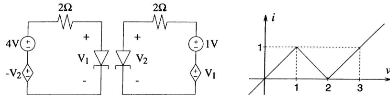
2i2 2Q
Figure 3.1: Tunnel diode circuit and the i — v characteristics of the tunnel diodes.
Then, we have overcome the convergence problem by making a small modification in the third step of the algorithm described above. Consequently, the final version of the third step of the POPCORN algorithm is given below.
3. Let lies in the linear region = {ofc+i,i, · · · > Ofc+i,m}· The new linear region CTjt+i = {afc+1,1, afc+i,2) · · ·, is chosen as follows: For j = 1,2, · · ·, m If j = Okj then
with probability 1 — q
Any other segment with probability q , 0 < 9 < 1
If ^ then
j with probability 1 — p
Any other segment with probability p , 0 < p < 1
W ith this modification, a segment may not be chosen, albeit with a very small probability
q, for the next iteration, even though the present solution satisfies limits of the segment. The POPCORN algorithm assures the convergence for any initial guess since the algorithm tries all of the linear regions eventually, until it converges. Having such a feature, it resembles the well-known simulated annealing algorithm without cooling [50]. The convergence proof is trivial, since the probability of visiting the linear region containing the solution is non-zero. In the worst case, the algorithm visits all of the linear regions and convergence is always assured. This simple proof does not tell us how fast the algorithm converges, it merely shows that it converges eventually. The important