Quasimetallic silicon micromachined photonic crystals
B. Temelkuran, Mehmet Bayindir, E. Ozbay, J. P. Kavanaugh, M. M. Sigalas et al.
Citation: Appl. Phys. Lett. 78, 264 (2001); doi: 10.1063/1.1339256 View online: http://dx.doi.org/10.1063/1.1339256
View Table of Contents: http://apl.aip.org/resource/1/APPLAB/v78/i3
Published by the American Institute of Physics.
Additional information on Appl. Phys. Lett.
Journal Homepage: http://apl.aip.org/
Journal Information: http://apl.aip.org/about/about_the_journal
Top downloads: http://apl.aip.org/features/most_downloaded
Information for Authors: http://apl.aip.org/authors
Quasimetallic silicon micromachined photonic crystals
B. Temelkuran,a)Mehmet Bayindir,b)and E. Ozbay
Department of Physics, Bilkent University, Bilkent 06533 Ankara, Turkey J. P. Kavanaugh, M. M. Sigalas, and G. Tuttle
Ames Laboratory and Microelectronics Research Center, Iowa State University, Ames, Iowa 50011 共Received 4 May 2000; accepted for publication 9 November 2000兲
We report on fabrication of a layer-by-layer photonic crystal using highly doped silicon wafers processed by semiconductor micromachining techniques. The crystals, built using 共100兲 silicon wafers, resulted in an upper stop band edge at 100 GHz. The transmission and defect characteristics of these structures were found to be analogous to metallic photonic crystals. We also investigated the effect of doping concentration on the defect characteristics. The experimental results agree well with predictions of the transfer matrix method simulations. © 2001 American Institute of Physics.
关DOI: 10.1063/1.1339256兴
Photonic crystals are periodic structures that can reflect electromagnetic共EM兲 waves in all directions within a certain frequency range. These structures can be used to control and manipulate the behavior of EM waves.1,2 Although earlier work concentrated on building these crystals with dielectric materials3,4there are certain advantages of introducing met-als to photonic crystmet-als.5–11
Various techniques have been reported for the fabrica-tion of dielectric layer-by-layer photonic crystals at different frequency regions,4,12,13 and recently at optical frequencies.14,15 However, limitations of the standard ma-chining techniques used to fabricate three-dimensional共3D兲 metallic photonic crystals restricted experimental demonstra-tions and technological applicademonstra-tions of these crystals to mi-crowave frequencies.9,16 3D metallic structures standing on dielectric supports operating at infrared wavelengths were also demonstrated.17,18However, these structures do not have the advantage of a band gap extending to zero frequency due to nontouching metallic layers. The fabrication of 3D metal-lic photonic crystals at higher共compared to microwave兲 fre-quency regions with a complete metallicity gap extending to zero frequency is still a challenge.
In this letter, we propose a method for the fabrication of layer-by-layer photonic crystals having metallic properties using silicon micromachining techniques. The touching lay-ers form a continuous network, in which the long wave-lengths cannot penetrate the conducting mesh, and the band gap extends to zero frequency. We have previously investi-gated the properties of such a metallic photonic crystal with an upper band edge at 20 GHz. The method allows the fab-rication of these structures at a frequency range extending from 100 GHz to 10 THz.
The layer-by-layer photonic crystal was fabricated using highly doped silicon 共100兲 wafers, which were 75 mm in diameter and 400 m thick. We predicted that, due to the low resistivity of the Si wafers共in the range of 0.0015–0.004
⍀ cm兲, this structure would show metallic photonic crystal
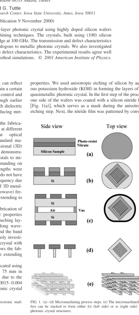
properties. We used anisotropic etching of silicon by aque-ous potassium hydroxide共KOH兲 in forming the layers of the quasimetallic photonic crystal. In the first step of the process, one side of the wafers was coated with a silicon nitride film
关Fig. 1共a兲兴, which serves as a mask during the anisotropic
etching step. Next, the nitride film was patterned by
conven-a兲Author to whom correspondence should be addressed; electronic mail:
b兲Electronic mail: [email protected]
FIG. 1. 共a兲–共d兲 Micromachining process steps. 共e兲 The micromachined wa-fers can be stacked to form either fct 共left side兲 or st 共right side兲 type photonic crystal structures.
APPLIED PHYSICS LETTERS VOLUME 78, NUMBER 3 15 JANUARY 2001
264
0003-6951/2001/78(3)/264/3/$18.00 © 2001 American Institute of Physics
tional photolithography and aqueous hydrofluoric 共HF兲 acid etching. After the silicon nitride layer is patterned 关Fig. 1共b兲兴, in order to protect back sides of the wafers, we bond each sample back to back with another patterned sample us-ing black wax共Apiezon-W兲 关Fig. 1共c兲兴. The wafers are then dipped into an aqueous KOH solution. A typical etch per-formed in a 25% KOH solution at a temperature of 55 °C takes about 24 h to etch entirely through the wafers. Finally, the wax is removed by trichloroethane 共TCA兲, so that the coupled layers bonded with wax are separated关Fig. 1共d兲, left side兴. The remaining nitride film is removed by HF, and the samples are ready to be stacked to form photonic crystals
关Fig. 1共d兲, right side兴. The pattern consists of 19 parallel
stripes共each 150m⫻400m⫻ 3 cm兲 with center-to-center separation of 1600m. These stripe dimensions and the wa-fer thickness determine the upper band edge, calculated to be around 100 GHz. As shown in Fig. 1共e兲, the wafers 共each a single layer of the quasimetallic photonic crystal兲 may be stacked to form a simple tetragonal 共st兲 or a face centered tetragonal共fct兲 crystals.
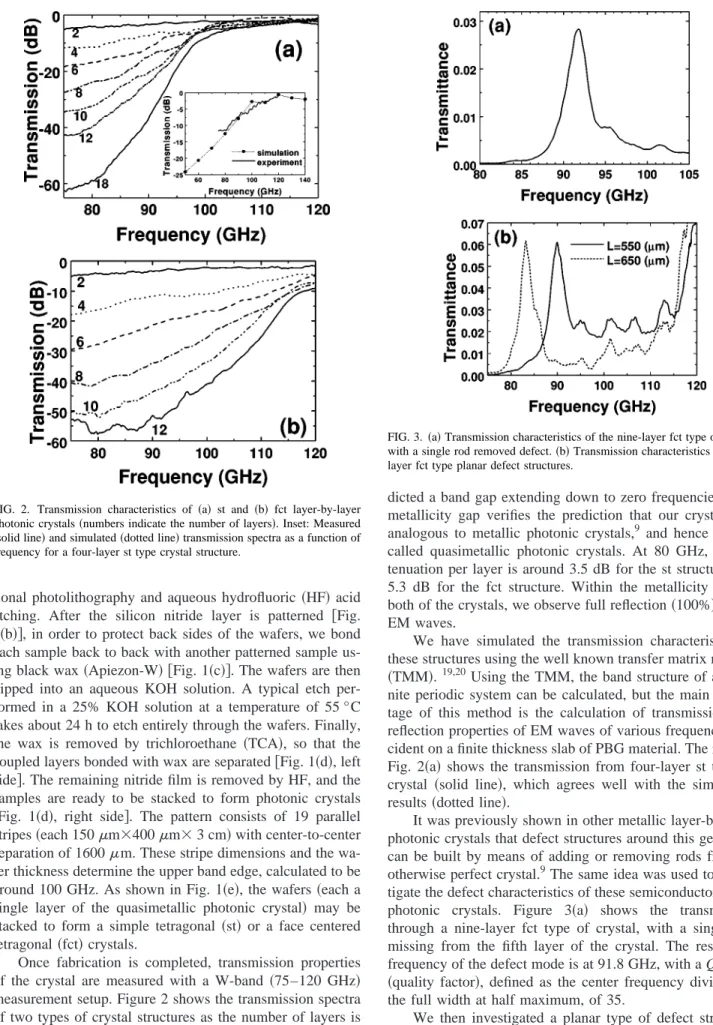
Once fabrication is completed, transmission properties of the crystal are measured with a W-band 共75–120 GHz兲 measurement setup. Figure 2 shows the transmission spectra of two types of crystal structures as the number of layers is increased. The upper edge of the band gap for st crystal is located at 100 GHz关Fig. 2共a兲兴, and for fct crystal at 115 GHz
关Fig. 2共b兲兴. No lower band edge is detected within the
mea-surable frequency range, consistent with the theory that
pre-dicted a band gap extending down to zero frequencies. This metallicity gap verifies the prediction that our crystals are analogous to metallic photonic crystals,9 and hence can be called quasimetallic photonic crystals. At 80 GHz, the at-tenuation per layer is around 3.5 dB for the st structure and 5.3 dB for the fct structure. Within the metallicity gap of both of the crystals, we observe full reflection共100%兲 of the EM waves.
We have simulated the transmission characteristics of these structures using the well known transfer matrix method
共TMM兲. 19,20Using the TMM, the band structure of an
infi-nite periodic system can be calculated, but the main advan-tage of this method is the calculation of transmission and reflection properties of EM waves of various frequencies in-cident on a finite thickness slab of PBG material. The inset in Fig. 2共a兲 shows the transmission from four-layer st type of crystal 共solid line兲, which agrees well with the simulation results 共dotted line兲.
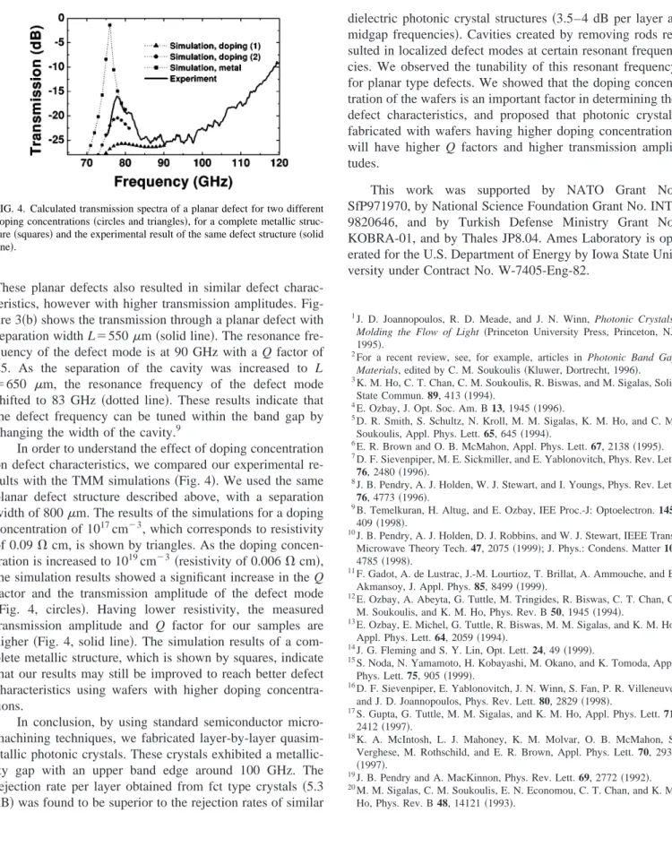
It was previously shown in other metallic layer-by-layer photonic crystals that defect structures around this geometry can be built by means of adding or removing rods from an otherwise perfect crystal.9The same idea was used to inves-tigate the defect characteristics of these semiconductor based photonic crystals. Figure 3共a兲 shows the transmission through a nine-layer fct type of crystal, with a single rod missing from the fifth layer of the crystal. The resonance frequency of the defect mode is at 91.8 GHz, with a Q factor
共quality factor兲, defined as the center frequency divided by
the full width at half maximum, of 35.
We then investigated a planar type of defect structure, built around an eight-layer fct based photonic crystal. The planar defect was obtained by separating the fourth and fifth layers of the crystal. This resulted in a planar air gap between the two photonic mirrors, each formed of a four layer crystal. FIG. 2. Transmission characteristics of 共a兲 st and 共b兲 fct layer-by-layer
photonic crystals共numbers indicate the number of layers兲. Inset: Measured
共solid line兲 and simulated 共dotted line兲 transmission spectra as a function of
frequency for a four-layer st type crystal structure.
FIG. 3. 共a兲 Transmission characteristics of the nine-layer fct type of crystal with a single rod removed defect.共b兲 Transmission characteristics of eight-layer fct type planar defect structures.
265 Appl. Phys. Lett., Vol. 78, No. 3, 15 January 2001 Temelkuranet al.
These planar defects also resulted in similar defect charac-teristics, however with higher transmission amplitudes. Fig-ure 3共b兲 shows the transmission through a planar defect with separation width L⫽550m共solid line兲. The resonance fre-quency of the defect mode is at 90 GHz with a Q factor of 25. As the separation of the cavity was increased to L
⫽650 m, the resonance frequency of the defect mode shifted to 83 GHz 共dotted line兲. These results indicate that the defect frequency can be tuned within the band gap by changing the width of the cavity.9
In order to understand the effect of doping concentration on defect characteristics, we compared our experimental re-sults with the TMM simulations共Fig. 4兲. We used the same planar defect structure described above, with a separation width of 800m. The results of the simulations for a doping concentration of 1017cm⫺3, which corresponds to resistivity of 0.09 ⍀ cm, is shown by triangles. As the doping concen-tration is increased to 1019cm⫺3共resistivity of 0.006 ⍀ cm兲, the simulation results showed a significant increase in the Q factor and the transmission amplitude of the defect mode
共Fig. 4, circles兲. Having lower resistivity, the measured
transmission amplitude and Q factor for our samples are higher 共Fig. 4, solid line兲. The simulation results of a com-plete metallic structure, which is shown by squares, indicate that our results may still be improved to reach better defect characteristics using wafers with higher doping concentra-tions.
In conclusion, by using standard semiconductor micro-machining techniques, we fabricated layer-by-layer quasim-etallic photonic crystals. These crystals exhibited a mquasim-etallic- metallic-ity gap with an upper band edge around 100 GHz. The rejection rate per layer obtained from fct type crystals 共5.3 dB兲 was found to be superior to the rejection rates of similar
dielectric photonic crystal structures 共3.5–4 dB per layer at midgap frequencies兲. Cavities created by removing rods re-sulted in localized defect modes at certain resonant frequen-cies. We observed the tunability of this resonant frequency for planar type defects. We showed that the doping concen-tration of the wafers is an important factor in determining the defect characteristics, and proposed that photonic crystals fabricated with wafers having higher doping concentrations will have higher Q factors and higher transmission ampli-tudes.
This work was supported by NATO Grant No. SfP971970, by National Science Foundation Grant No. INT-9820646, and by Turkish Defense Ministry Grant No. KOBRA-01, and by Thales JP8.04. Ames Laboratory is op-erated for the U.S. Department of Energy by Iowa State Uni-versity under Contract No. W-7405-Eng-82.
1
J. D. Joannopoulos, R. D. Meade, and J. N. Winn, Photonic Crystals:
Molding the Flow of Light共Princeton University Press, Princeton, NJ,
1995兲.
2For a recent review, see, for example, articles in Photonic Band Gap
Materials, edited by C. M. Soukoulis共Kluwer, Dortrecht, 1996兲.
3K. M. Ho, C. T. Chan, C. M. Soukoulis, R. Biswas, and M. Sigalas, Solid State Commun. 89, 413共1994兲.
4E. Ozbay, J. Opt. Soc. Am. B 13, 1945共1996兲. 5
D. R. Smith, S. Schultz, N. Kroll, M. M. Sigalas, K. M. Ho, and C. M. Soukoulis, Appl. Phys. Lett. 65, 645共1994兲.
6E. R. Brown and O. B. McMahon, Appl. Phys. Lett. 67, 2138共1995兲. 7D. F. Sievenpiper, M. E. Sickmiller, and E. Yablonovitch, Phys. Rev. Lett.
76, 2480共1996兲.
8
J. B. Pendry, A. J. Holden, W. J. Stewart, and I. Youngs, Phys. Rev. Lett.
76, 4773共1996兲.
9B. Temelkuran, H. Altug, and E. Ozbay, IEE Proc.-J: Optoelectron. 145, 409共1998兲.
10
J. B. Pendry, A. J. Holden, D. J. Robbins, and W. J. Stewart, IEEE Trans. Microwave Theory Tech. 47, 2075共1999兲; J. Phys.: Condens. Matter 10, 4785共1998兲.
11F. Gadot, A. de Lustrac, J.-M. Lourtioz, T. Brillat, A. Ammouche, and E. Akmansoy, J. Appl. Phys. 85, 8499共1999兲.
12
E. Ozbay, A. Abeyta, G. Tuttle, M. Tringides, R. Biswas, C. T. Chan, C. M. Soukoulis, and K. M. Ho, Phys. Rev. B 50, 1945共1994兲.
13E. Ozbay, E. Michel, G. Tuttle, R. Biswas, M. M. Sigalas, and K. M. Ho, Appl. Phys. Lett. 64, 2059共1994兲.
14J. G. Fleming and S. Y. Lin, Opt. Lett. 24, 49共1999兲. 15
S. Noda, N. Yamamoto, H. Kobayashi, M. Okano, and K. Tomoda, Appl. Phys. Lett. 75, 905共1999兲.
16D. F. Sievenpiper, E. Yablonovitch, J. N. Winn, S. Fan, P. R. Villeneuve, and J. D. Joannopoulos, Phys. Rev. Lett. 80, 2829共1998兲.
17
S. Gupta, G. Tuttle, M. M. Sigalas, and K. M. Ho, Appl. Phys. Lett. 71, 2412共1997兲.
18K. A. McIntosh, L. J. Mahoney, K. M. Molvar, O. B. McMahon, S. Verghese, M. Rothschild, and E. R. Brown, Appl. Phys. Lett. 70, 2937
共1997兲.
19
J. B. Pendry and A. MacKinnon, Phys. Rev. Lett. 69, 2772共1992兲. 20M. M. Sigalas, C. M. Soukoulis, E. N. Economou, C. T. Chan, and K. M.
Ho, Phys. Rev. B 48, 14121共1993兲.
FIG. 4. Calculated transmission spectra of a planar defect for two different doping concentrations共circles and triangles兲, for a complete metallic struc-ture共squares兲 and the experimental result of the same defect structure 共solid line兲.
266 Appl. Phys. Lett., Vol. 78, No. 3, 15 January 2001 Temelkuranet al.