On the effect of
N-GaN/P-GaN/N-GaN/P-GaN/N-GaN built-in junctions in the n-N-GaN/P-GaN/N-GaN/P-GaN/N-GaN layer for
InGaN/GaN light-emitting diodes
Zabu Kyaw,1,5 Zi-Hui Zhang,1,5 Wei Liu,1 Swee Tiam Tan,1 Zhen Gang Ju,1 Xue Liang Zhang,1 Yun Ji,1 Namig Hasanov,1 Binbin Zhu,1 Shunpeng Lu,1 Yiping Zhang,1 Xiao
Wei Sun,1,3,6 and Hilmi Volkan Demir1,2,4,*
1LUMINOUS! Centre of Excellence for Semiconductor Lighting and Displays, School of Electrical and Electronic
Engineering, Nanyang Technological University, 50 Nanyang Avenue, 639798, Singapore
2School of Physics and Mathematical Sciences, Nanyang Technological University, 21 Nanyang Link, 637371,
Singapore
3Department of Electronics and Electrical Engineering, South University of Science and Technology of China,
Shenzhen, Guangdong, 518055, China
4Department of Electrical and Electronics, Department of Physics, and UNAM–Institute of Material Science and
Nanotechnology, Bilkent University, TR-06800, Ankara, Turkey
5Authors of equal contribution
6[email protected] *[email protected]
Abstract: N-GaN/P-GaN/N-GaN/P-GaN/N-GaN (NPNPN-GaN) junctions
embedded between the n-GaN region and multiple quantum wells (MQWs) are systematically studied both experimentally and theoretically to increase the performance of InGaN/GaN light emitting diodes (LEDs) in this work. In the proposed architecture, each thin P-GaN layer sandwiched in the NPNPN-GaN structure is completely depleted due to the built-in electric field in the NPNPN-GaN junctions, and the ionized acceptors in these P-GaN layers serve as the energy barriers for electrons from the n-GaN region, resulting in a reduced electron over flow and enhanced the current spreading horizontally in the n- GaN region. These lead to increased optical output power and external quantum efficiency (EQE) from the proposed device.
©2014 Optical Society of America
OCIS codes: (230.3670) Light-emitting diodes; (230.5590) Quantum-well, -wire and -dot
devices; (160.6000) Semiconductor materials.
References and links
1. S. T. Tan, X. W. Sun, H. V. Demir, and S. P. DenBaars, “Advances in the LED materials and architectures for energy-saving solid-state lighting toward “light revolution”,” IEEE Photonics J. 4(2), 613–619 (2012). 2. R. A. Arif, Y.-K. Ee, and N. Tansu, “Polarization engineering via staggered InGaN quantum wells for radiative
efficiency enhancement of light emitting diodes,” Appl. Phys. Lett. 91(9), 091110 (2007).
3. R. A. Arif, H. Zhao, and N. Tansu, “Type-II InGaN-GaNAs quantum wells for lasers applications,” Appl. Phys. Lett. 92(1), 011104 (2008).
4. H. Zhao, R. A. Arif, and N. Tansu, “Self-consistent gain analysis of type-II ‘W’ InGaN–GaNAs quantum well lasers,” J. Appl. Phys. 104(4), 043104 (2008).
5. H. Zhao, G. Liu, R. A. Arif, and N. Tansu, “Current injection efficiency induced efficiency-droop in InGaN quantum well light-emitting diodes,” Solid State Electron. 54(10), 1119–1124 (2010).
6. M. H. Kim, M. F. Schubert, Q. Dai, J. K. Kim, E. F. Schubert, J. Piprek, and Y. Park, “Origin of efficiency droop in GaN-based light-emitting diodes,” Appl. Phys. Lett. 91(18), 183507 (2007).
7. Y.-K. Kuo, J.-Y. Chang, and M.-C. Tsai, “Enhancement in hole-injection efficiency of blue InGaN light-emitting diodes from reduced polarization by some specific designs for the electron blocking layer,” Opt. Lett. 35(19), 3285–3287 (2010).
8. S.-H. Yen, M.-C. Tsai, M.-L. Tsai, Y.-J. Shen, T.-C. Hsu, and Y.-K. Kuo, “Effect of n-type AlGaN layer on carrier transportation and efficiency droop of blue InGaN light-emitting diodes,” IEEE Photonics Technol. Lett.
9. J. Han, K. E. Waldrip, S. R. Lee, J. J. Figiel, S. J. Hearne, G. A. Petersen, and S. M. Myers, “Control and elimination of cracking of AlGaN using low-temperature AlGaN interlayers,” Appl. Phys. Lett. 78(1), 67–70 (2001).
10. J. M. Bethoux, P. Vennegues, F. Natali, E. Feltin, O. Tottereau, G. Nataf, P. De Mierry, and F. Semond, “Growth of high quality crack-free AlGaN films on GaN templates using plastic relaxation through buried cracks,” J. Appl. Phys. 94(10), 6499–6508 (2003).
11. H. Y. Ryu and J. I. Shim, “Effect of current spreading on the efficiency droop of InGaN light-emitting diodes,” Opt. Express 19(4), 2886–2894 (2011).
12. X. Guo and E. F. Schubert, “Current crowding in GaN/InGaN light emitting diodes on insulating substrates,” J. Appl. Phys. 90(8), 4191–4195 (2001).
13. L. Zhou, W. Lanford, A. T. Ping, I. Adesida, J. W. Yang, and A. Khan, “Low resistance Ti/Pt/Au ohmic contacts to p-type GaN,” Appl. Phys. Lett. 76(23), 3451–3453 (2000).
14. L.-C. Chen, J.-K. Ho, C.-S. Jong, C. C. Chiu, K.-K. Shih, F.-R. Chen, J.-J. Kai, and L. Chang, “Oxidized Ni/Pt and Ni/Au ohmic contacts to p-type GaN,” Appl. Phys. Lett. 76(25), 3703–3706 (2000).
15. J. K. Sheu, G. C. Chi, and M. J. Jou, “Enhanced output power in an InGaN–GaN multiquantum-well light-emitting diode with an InGaN current-spreading layer,” IEEE Photonics Technol. Lett. 13(11), 1164–1166 (2001).
16. H.-H. Liu, P.-R. Chen, G.-Y. Lee, and J.-I. Chyi, “Efficiency enhancement of InGaN LEDs with an n-type AlGaN/GaN/InGaN current spreading layer,” IEEE Electron. Device Lett. 32(10), 1409–1411 (2011). 17. Z.-H. Zhang, S. T. Tan, W. Liu, Z. Ju, K. Zheng, Z. Kyaw, Y. Ji, N. Hasanov, X. W. Sun, and H. V. Demir,
“Improved InGaN/GaN light-emitting diodes with a p-GaN/n-GaN/p-GaN/n-GaN/p-GaN current-spreading layer,” Opt. Express 21(4), 4958–4969 (2013).
18. Z.-H. Zhang, S. T. Tan, Z. Kyaw, Y. Ji, W. Liu, Z. Ju, N. Hasanov, X. W. Sun, and H. V. Demir, “InGaN/GaN light-emitting diode with a polarization tunnel junction,” Appl. Phys. Lett. 102(19), 193508 (2013).
19. Z. G. Ju, S. T. Tan, Z.-H. Zhang, Y. Ji, Z. Kyaw, Y. Dikme, X. W. Sun, and H. V. Demir, “On the origin of the redshift in the emission wavelength of InGaN/GaN blue light emitting diodes grown with a higher temperature interlayer,” Appl. Phys. Lett. 100(12), 123503 (2012).
20. Z.-H. Zhang, S. T. Tan, Z. G. Ju, W. Liu, Y. Ji, Z. Kyaw, Y. Dikme, X. W. Sun, and H. V. Demir, “On the effect of step-doped quantum barriers in InGaN/GaN light emitting diodes,” J. Disp. Technol. 9(4), 226–233 (2013). 21. Z. Gong, S. Jin, Y. Chen, J. McKendry, D. Massoubre, I. M. Watson, E. Gu, and M. D. Dawson,
“Size-dependent light output, spectral shift, and self-heating of 400 nm InGaN light-emitting diodes,” J. Appl. Phys.
107(1), 013103 (2010).
22. D. Han, J. Shim, D. S. Shin, E. Nam, and H. Park, “Effect of temperature distribution and current crowding on the performance of lateral GaN-based light-emitting diodes,” Phys. Status Solidi C 7(7–8), 2133–2135 (2010). 23. S. M. Sze, Physics of Semiconductor Devices, 2nd ed. (John Wiley, 1981).
24. H. Tokunaga, A. Ubukata, Y. Yano, A. Yamaguchi, N. Akutsu, T. Yamasaki, and K. Matsumoto, “Effects of growth pressure on AlGaN and Mg-doped GaN grown using multiwafer metal organic vapor phase epitaxy system,” J. Cryst. Growth 272(1–4), 348–352 (2004).
25. B. J. Baliga, Fundamentals of Power Semiconductor Devices (Springer, 2008).
1. Introduction
InGaN/GaN light-emitting diodes (LEDs) have been widely used in liquid crystal display (LCD) backlighting and full color displays and increasingly in indoor and outdoor lighting. Tremendous effort has been devoted to the improvement of LED performance through material and device engineering [1]. Some of the main issues affecting the LED performance and the corresponding solutions reported in the literature include: (1) Polarization induced quantum confined Stark effect (QCSE) in quantum wells (QWs) separates electrons and holes spatially and reduces the optical matrix element. Staggered InGaN QWs [2] and type-II QWs [3, 4] have been proposed to improve the optical matrix element. (2) Electron overflow from the QWs to the p-GaN region gives rise to the quantum efficiency droop at high current density [5, 6]. A p-type AlGaN electron blocking layer (EBL) is used to block electrons from escaping to the p-GaN region [7]. Moreover, an n-type AlGaN layer inserted below the active region for the reduction of the electron overflow has also been proposed [8–10]. (3) Current crowding effect for InGaN/GaN LEDs grown on insulating sapphire substrates with lateral current injection scheme causes non-uniform light emission across the device area and reduces the quantum efficiency [11, 12]. It has been reported that improving the p-type specific contact resistance helps to achieve a better current spreading [13, 14]. Meanwhile, it has been also shown that the current crowding decreases when the device is more resistive vertically [12], and an n-type InGaN current spreading layer has therefore been proposed to realize a better current spreading [15, 16]. Due to the relatively low growth temperature the
crystal quality of the n-type InGaN current spreading layer would be inferior to that of high-temperature grown GaN, which may give rise to non-radiative recombination defects. Recently, a new design of p-GaN/n-GaN/p-GaN/n-GaN/p-GaN (PNPNP-GaN) current spreading layers in the p-GaN region proved to be effective in enhancing the optical power and external quantum efficiency (EQE) [17] by increasing the current spreading through generating energy barriers for holes. The limitations of the thickness (typically less than 250 nm) and the growth temperature of the p-GaN region (much lower than the growth temperature of n-GaN) in InGaN LEDs imposes constrains on the freedom of optimizing the growth of the PNPNP-GaN and, thus, to its effectiveness on the current spreading enhancement.
In this work we propose a new design compromising of lattice matched NPNPN-GaN junctions in the n-GaN region that serve both as the current spreading layer and the electron blocking layer. Since the growth temperature of the NPNPN-GaN junctions in the n-GaN region is not limited to be lower unlike in the case of PNPNP-GaN junctions in the p-GaN region or the n-type InGaN, an excellent crystal quality of the NPNPN-GaN junctions in the n-GaN region can be maintained. Moreover, because there is no practical limit on the thickness of the NPNPN-GaN junctions in the n-GaN region, there is a larger room for optimizing the growth. The NPNPN-GaN junctions in the n-GaN region with these advantages hold great promise for improving the InGaN/GaN LED performance. Here, we have proved the effectiveness of the NPNPN-GaN junctions in the n-GaN region for the enhancement of the LED performance both experimentally and theoretically. In the theoretical simulations, the APSYS simulation program has been used to solve self-consistently the Poisson’s equations, continuity equations, and Schrӧdinger equation with proper boundary conditions. The parameters used in the simulations can be found elsewhere [18].
2. Experiments
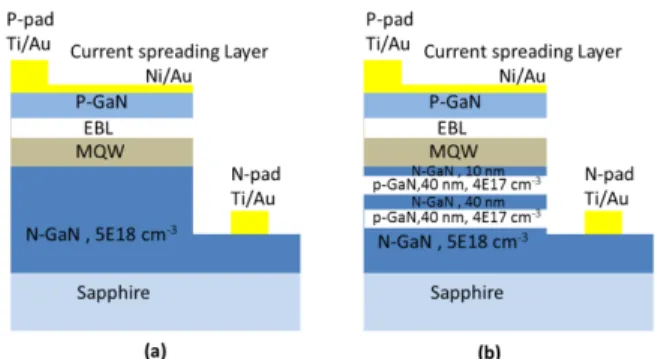
In our study, two InGaN/GaN LEDs were grown by metal-organic chemical vapor deposition (MOCVD) system as shown in Fig. 1(a) for the reference device and Fig. 1(b) for the proposed device dubbed the NPNPN-GaN device. The epitaxial growth of the two LEDs was initiated on c-sapphire substrates. Both LEDs consist of a 4 µm thick unintentionally doped GaN (u-GaN) layer grown on a 30 nm GaN buffer layer, and then followed by a 2 µm thick
Si-doped GaN layer (n-GaN region) with a doping concentration of 5 × 1018 cm−3. For the
reference device, five-period In0.18Ga0.82N/GaN MQWs with a 3 nm thick well and a 12 nm
thick barrier were grown after the n-GaN. For the NPNPN-GaN device, the NPNPNP-GaN junctions were grown before the MQWs. The thickness of the N-GaN layer (with Si doping
concentration of Nd = 5 × 1018 cm−3) and the P-GaN layer (with ionized Mg concentration of
Na = 4 × 1017 cm−3) for each NPN-GaN junction was 40 nm each. Then, the same
In0.18Ga0.82N/GaN MQWs as in the reference device were grown after the NPNPN-GaN
junctions. Both the reference device and the NPNPN-GaN device had a 25 nm
Mg-doped-Al0.15Ga0.85N layer serving as the EBL, followed by a 200 nm thick Mg-doped GaN (p-GaN)
region with an effective hole concentration of 3 × 1017 cm −3.
The LED chips were fabricated using standard fabrication process for the two devices. LED mesa of 350 µm × 350 µm was patterned through reactive ion etching. Ni/Au (5 nm/5 nm) was deposited as the semi-transparent current spreading layer on the defined
mesa and then the thermal annealing was performed in the mixture of N2 and O2 for 5 min at a
temperature of 525 ̊C. Finally, Ti/Au (30 nm/150 nm) was deposited on the exposed n-GaN layer and the semi-transparent current spreading layer as the N and P electrodes [17–20]. The electroluminescence (EL) spectra and the optical output power for both the devices were collected through an integrating sphere attached to an Ocean Optics spectrometer (QE65000).
Fig. 1. Schematic diagrams of (a) the reference device and (b) the proposed NPNPN-GaN device.
3. Results and discussion
As shown in Figs. 2(a) and 2(b), the electroluminescence (EL) spectra are presented at different injection currents of 20, 50, 100 and 150 mA for the reference device and the NPNPN-GaN device, respectively. A stronger EL intensity is evident from the NPNPN-GaN device compared to the reference device. Meanwhile, a red shift of the emission wavelength is observed with respect to the increasing injection current for both of the devices. This is commonly observed and attributed to the increased junction temperature due to the heating effect [21, 22]. 405 420 435 450 465 480 495 0 100 200 300 400 500 600 700 800 900 1000 E L in te ns it y (a u) Wavelength (nm) 20mA 50mA 100mA 150mA 150mA 20mA
(a) Reference Device
405 420 435 450 465 480 495 0 100 200 300 400 500 600 700 800 900 1000 150mA EL inten sity (au ) Wavelength (nm) 20mA 50mA 100mA 150mA 20mA (b) NPNPN Device
Fig. 2. EL spectra measured from (a) the reference device and (b) the NPNPN-GaN device.
The measured optical power and EQE are shown in Fig. 3. It can be seen that an improved optical power and EQE have been achieved from the NPNPN-GaN device compared to that of the reference device. For example, the power enhancement from the NPNPN-GaN device relative to the reference device is about 30% at 150 mA according to Fig. 3.
0 10 20 30 40 50 60 70 80 90 100 110 120 130 140 150 0 4 8 12 16 20 24 28 32 36 O p ti ca l pow er (mW) EQ E (%) Current (mA) NPNPN Reference 0 4 8 12 16 20 24 28 32 36
Fig. 3. Optical output power and EQE measured as a function of the current injection for the reference device and the proposed NPNPN-GaN device.
Improvement of the optical output power and EQE for the NPNPN-GaN device could be attributed to two reasons. First, the electron overflow is reduced due to the blocking barriers generated in the NPNPN-GaN junctions. Second, the current crowding is reduced due to the fact that the NPNPN-GaN junctions increase the layer resistivity vertically and thus promote the lateral current spreading.
To reveal the physical mechanism of the NPNPN-GaN junctions and their effect on the device performance, APSYS was used to simulate the band structures, electron and hole concentration distributions and radiative recombination rates in the MQWs for both of the devices. Figures 4(a) and 4(b) show the simulated energy band profiles for the reference device and the NPNPN-GaN device, respectively. The significant difference in the energy band profile for the two devices lies in the section of the conduction band of the n-GaN region in contrast to the flat band of the reference device; there are two energy barriers generated after incorporating the NPNPN-GaN junctions.
0.45 0.50 0.55 0.60 0.65 0.70 0.75 0.80 -0.5 0.0 0.5 1.0 1.5 2.0 2.5 3.0 3.5 4.0 N-GaN Efh Efe Ev P-GaN Ene rgy ( e V)
Relative position (um) MQWs
EBL No barriers for electron
Ec C+ (a) 0.45 0.50 0.55 0.60 0.65 0.70 0.75 0.80 -0.5 0.0 0.5 1.0 1.5 2.0 2.5 3.0 3.5 4.0 Efh Ev En er g y ( eV)
Relative position (um) C+
N-GaN P-GaN N-GaN P-GaN N-GaN MQWs
EBL P-GaN (b) Barriers for electron
Ec Efe
Fig. 4. Energy band diagram at 20 A/cm2 for (a) the reference device and (b) the NPNPN-GaN
device. Ec, Ev, Efe and Efh denote the conduction band, valance band, and quasi-Fermi level for
electrons and holes, respectively.
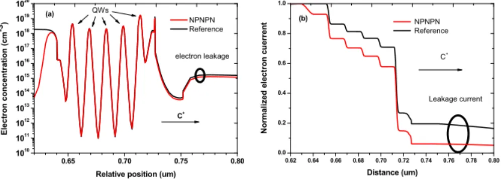
These energy barriers are helpful for the electron overflow reduction [8]. This can be confirmed with the comparison of the simulated electron concentration distribution and the normalized electron current for the two devices as shown in Figs. 5(a) and 5(b). The electron concentration of the NPNPN-GaN device is much lower than that of the reference device in the p-GaN region and so is the normalized electron current.
0.65 0.70 0.75 0.80 1010 1011 1012 1013 1014 1015 1016 1017 1018 1019 1020 El e ctr on c once n tr ati o n (cm -3)
Relative position (um) NPNPN Reference C+ QWs electron leakage (a) 0.62 0.64 0.66 0.68 0.70 0.72 0.74 0.76 0.78 0.80 0.0 0.2 0.4 0.6 0.8 1.0 N o rm al ized el ec tr on cu er re nt Distance (um) NPNPN Reference Leakage current C+ (b)
Fig. 5. Simulated (a) electron concentration and (b) normalized electron current at 20 A/cm2
across the InGaN/GaN MQWs region for the reference device and the NPNPN-GaN device, respectively.
The NPNPN-GaN junctions can also reduce the current crowding and thus promote the lateral current spreading. As the energy barriers for the electrons in the conduction band of the
n-GaN region have been generated, the NPNPN-GaN junctions increase the layer resistivity vertically, which is beneficial for better current spreading [15–17]. Figures 6(a) and 6(b) depict the simplified equivalent circuits of the reference device and the NPNPN-GaN device. In the reference device grown on the insulating substrates with the lateral current-injection scheme, the current flows both vertically and laterally from the p-GaN region to the n-GaN region. However, the current preferably flows vertically due to the much smaller sheet resistance of the n-GaN region compared to the p-GaN region. This leads to the non-uniform current distribution (i.e., I1 > I2 > I3 > I4 > ... > In), which is root reason for the current crowding effect [12]. This detrimental current crowding effect can be suppressed by incorporating the GaN junctions in the LED structure. In the case of the
NPNPN-GaN device, we divide the total current into a vertical portion (J1) and a horizontal portion
(J2). Based on the equivalent circuits in Figs. 6(a) and 6(b), the simplified equations, Eq. (1)
and Eq. (2), are obtained.
1 2 1 CSL CSL p GaN npn p CSL CSL w t J N J lw ρ t ρ ρ ρ − = + + (1) 1 2 1 p GaN npn p CSL CSL J N J ρ t ρ ρ− ρ ≅ + (2)
where wCSL is the width of the current spreading layer and tCSL is the thickness of the current
spreading layer, w is the width of the device mesa, l is the length of the device mesa, tp is the
thickness of the p-GaN region, ρp-GaN and ρCSL are the resistivities for the p-GaN region and
the current spreading layer, respectively, and ρnpn is the specific interfacial resistivity induced
by the barrier height in each NPN-GaN junction [17]. N is the total number of NPN-GaN
junctions. From Eq. (2), obviously the lateral current (i.e., J2) can be improved by a higher
ratio of N × ρnpn / ρCSL, which can be achieved through either increasing N × ρnpn or reducing
ρCSL. Therefore, the current crowding effect can be suppressed by incorporating the
NPNPN-GaN junctions in the LED structure. It is noted that the current spreading effect will also be
enhanced by properly increasing the p-GaN region thickness tp as shown in Eq. (2).
Fig. 6. (a) Equivalent circuit of an InGaN/GaN LED grown on an insulating substrate (e.g., sapphire) using Ni/Au current spreading layer with lateral current-injection scheme
(I1 > I2 > I3 > I4 > ... > In) [17], and (b) simplified equivalent circuit of the InGaN/GaN LED
with possible current paths (J1 and J2) when the NPNPN-GaN junctions is embedded, using
Ni/Au as the current spreading layer on the top [17].
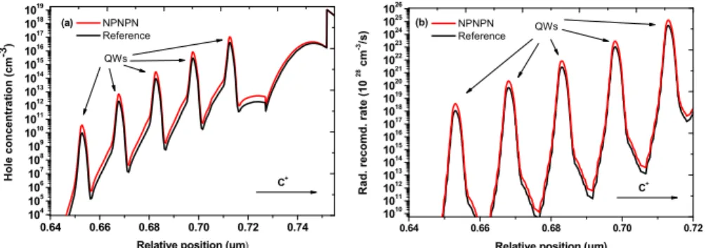
The improved current spreading effect by incorporating the NPNPN-GaN junctions brings about another benefit of higher efficiency of hole injection into the MQWs, which is confirmed by the simulated hole concentration distribution as shown in Fig. 7(a). The combined effects of the electron overflow reduction, the current crowding suppression, and
the hole injection enhancement with the application of the NPNPN-GaN junctions therefore enhance the radiative recombination rate, as shown in Fig. 7(b), which explains the enhancements of the optical output power and the EQE in the NPNPN-GaN device.
0.64 0.66 0.68 0.70 0.72 0.74 104 105 106 107 108 109 1010 1011 1012 1013 1014 1015 1016 1017 1018 1019 H o le co n cen tr a tio n ( cm -3)
Relative position (um) NPNPN Reference QWs C+ (a) 0.64 0.66 0.68 0.70 0.72 1010 1011 1012 1013 1014 1015 1016 1017 1018 1019 1020 1021 1022 1023 1024 1025 1026 NPNPN Reference Rad . re co m d . ra te (10 28 cm -3/s )
Relative position (um) QWs
C+
(b)
Fig. 7. Simulated (a) hole concentration and (b) radiative recombination rates at 20 A/cm2
across the InGaN/GaN MQW region for the reference device and the NPNPN-GaN device, respectively.
Figure 8 shows the current-voltage (I-V) characteristics of the two devices. Clearly we can see that the NPNPN-GaN device exhibits an increased forward voltage when compared to the reference device. The forward voltages of the reference device and the NPNPN-GaN device at 20 mA are 4.8 and 5.4 V, respectively. The increased forward voltage is likely due to the voltage drop across the NPNPN-GaN junctions as shown below. Due to the small thickness of each layer in the N-P-N junction, an abrupt junction model can be applied and the built-in potential in the P-GaN/N-GaN junction can be calculated to be 3.28 V using Eq. (3)
2 ln a d bi i N N kT V e N = (3)
where e is the elementary electron charge and Ni = 1.9 × 10⁻¹⁰ cm−3 for GaN. Therefore, the
total depletion region width is 93.39 nm according to the Eq. (4)
(
)
0 2 r 1/ a 1/ d bi t N N V W e ε ε + = (4)where εr = 8.9 for GaN and εo is the absolute dielectric constant [23]. This depletion region
consists of the depletion region width in P-GaN of 86.47 nm and the depletion region width in N-GaN layer of 6.91 nm, respectively, with the assumption that P-GaN and N-GaN layers have infinite lengths. However, the P-GaN layer has the actual thickness of only 40 nm; so, the depletion region extends through the whole P-GaN layer. It is also worthy to note that ionization ratio of the Mg dopants at room temperature is 1% in GaN [24]. According to the charge neutrality principle in the depletion region of a homojunction, the actual depletion width in N-GaN of NPN-GaN junction is only about 2.95 nm. Hence, the current can flow through the reversely biased junction when it was in reach through breakdown situation. The reach through breakdown voltage for the reversely biased junction is calculated according to Eq. (5) 2 0 2 a p RT r eN W BV ε ε = (5)
where Wp is the width of P-GaN [25]. A value of 0.65 V is obtained, which is found close to
the increment of the forward voltage in the NPNPN-GaN device. The NPNPN-GaN junctions can be further optimized by tuning the thickness, doping concentrations and the periods of NPN-GaN junctions, so that the improved current spreading can overwhelm the increased forward voltage, and thus an improved electrical performance can be realized.
0 1 2 3 4 5 6 7 8 9 10 11 12 13 14 15 0 10 20 30 40 50 60 70 80 90 100 Curren t (m A) Voltage (V) NPNPN Reference
Fig. 8. Measured I-V characteristics of the reference device and the NPNPN-GaN device.
4. Conclusion
In conclusion, the InGaN/GaN LED with a new design architecture of NPNPN-GaN junctions inserted between the n-GaN and the InGaN/GaN MQWs has been proposed and studied in this work. The experimental and theoretical findings indicate that the NPNPN-GaN junctions mitigate the electron overflow and reduce the current crowding effect. As the result, the optical power and EQE can be significantly improved. This work offers an alternative way to improve the carrier balancing and, thus, the LED performance.
Acknowledgments
We gratefully acknowledge that this work is supported by the Singapore National Research Foundation under Grant No. NRF-RF-2009-09 and NRF-CRP-6-2010-2 and the Singapore Agency for Science, Technology and Research (A*STAR) SERC under Grant No. 112-120-2009.