·
·
−
Appl Phys A (2009) 94: 73–82 DOI 10.1007/s00339-008-4939-7
The influence of nitridation time on the structural properties
of GaN grown on Si (111) substrate
Engin Arslan · Mustafa K. Ozturk · Özgür Duygulu · Ali Arslan Kaya · Suleyman Ozcelik · Ekmel Ozbay
Received: 31 July 2008 / Accepted: 13 October 2008 / Published online: 30 October 2008 © Springer-Verlag 2008
Abstract In the present paper, the effect of in-situ substrate nitridation time on crystalline quality of GaN films grown on Si (111) substrates by metal organic chemical vapor de- position (MOCVD) were investigated. A thin buffer layer of silicon nitride (SiNx ) with various thicknesses was achieved
through the nitridation of substrate at different nitiridation times ranging from 0 to 660 s. The structural characteristics, such as dislocation densities, correlation lengths of colum- nar crystallites, the tilt and twist of the mosaic structure, and the angles of rotational disorder, were all studied in detail by using a planar and cross-sectional view of high resolution transmission electron microscopy (HRTEM) and X-ray dif- fraction (HRXRD) performed at different scattering geome- tries. It was found that the dislocation densities, lateral co- herence lengths, vertical coherence lengths, and the tilt and
E. Arslan (
rsi
) E. OzbayNanotechnology Research Center, Department of Physics, Department of Electrical and Electronics Engineering, Bilkent University, Bilkent, 06800 Ankara, Turkey
e-mail: [email protected] Fax: +90-312-2901015
M.K. Ozturk S. Ozcelik
Department of Physics, Faculty of Science and Arts, Gazi University, Teknikokullar, 06500 Ankara, Turkey M.K. Ozturk
Department of Mineral Analysis and Technology, MTA, 06520 Ankara, Turkey
Ö. Duygulu
TUBITAK Marmara Research Center, Materials Institute, P.O. Box 21 Gebze Kocaeli, 41470, Kocaeli, Turkey A.A. Kaya
Engineering Faculty, Metallurgy and Materials Eng. Dept., Mugla University, 48170 Mugla, Turkey
twist of mosaic blocks in GaN films monotonically varies with the nitridation time. The experimental findings showed that the nitridation times had more influence on edge dislo- cation densities than the screw type.
PACS 61.05.Cp · 61.72.Uj · 64.70.Kg · 68.37.Lp · 68.37.Og · 72.80.Ey · 78.55.Cr
1 Introduction
The large direct band-gap and good thermal stability proper- ties of the GaN and related materials has enabled their poten- tial use in applications for laser diodes (LDs), visible-blind ultraviolet (UV) detectors, and short-wave light-emitting diodes (LEDs) [1–4]. However, there is still a lack of a suit- able substrate for GaN-based devices to fully exploit their superior properties. Thus far, there have been a large num- ber of studies concerned with the growth of GaN films on highly lattice-mismatched substrates, such as sapphire [5], SiC [6], or Si [7]. Among these materials, silicon has many advantages compared to SiC and sapphire due to its high crystal quality, low cost, good electrical and thermal con- ductivity, and large-area size as a substrate for the growth of GaN, AlGaN epitaxial layers [8, 9].
However, the growth of GaN films on a Si wafer is usu- ally associated with such problems as cracking in the epi- taxial layer because of large mismatches in the lattice pa- rameters ( 16.9%) and thermal expansion coefficients (ap- prox. 113%) [5, 7, 10–13]. Due to a large lattice mismatch, a high density of threading dislocations on the order of (109–1010 cm−2) exists in the GaN film on silicon sub- strates, which significantly affects the performance of the
∼ GaN based devices [8]. In order to obtain crack-free high- quality GaN film on Si substrate, various types of buffer lay- ers and growth conditions as well as post-growth heat treat- ment processes have been proposed by different research groups [10–17]. However, the appearance of the cracks is quite random on the film, which produces significant diffi- culty in device applications. Therefore, the control of crack distribution for a large area film is the main issue of the present study [7–11].
It has been recently demonstrated that defect-free GaN on Si could be realized when a Six Ny buffer was used in
hot wall chemical vapor deposition [14] with MOCVD [15] growth techniques. These buffer layers were achieved by ni- tridating the Si substrate with N2 flow at 900°C by Huang et al. [14] and at 1120°C by Wu-Yih Uena et al. [15]. With a similar approach, a double-buffer structure of AlN/Six Ny
was used to obtain high quality GaN film on Si substrate by using molecular beam epitaxy (MBE) [16]. The single- crystalline SiNx was obtained by introducing the active ni-
trogen plasma to the Si (111) surface at 900°C for approx- imately 30 s. Hageman et al. [17] reported significant im- provements on the optical and structural properties of the 1 μm GaN layer with the creation of a SiNx intermediate
layer.
Large lattice mismatch with respect to the substrate com- monly causes high dislocation densities in heteroepitaxial thin films [18–21]. These types of structures are often de- scribed by the model of mosaic crystals [20, 22]. The lateral and vertical dimensions of the crystallites are given by the lateral and vertical coherence length. The angular mismatch of the crystallites causes a tilt and twist, describing the angu- lar distribution of the crystallographic orientation of the mo- saic blocks perpendicular to, and within, the growth plane. Knowledge of all these structural parameters in detail is cru- cial in order to understand the microstructural properties of the grown epilayers, to optimize the growth conditions, and the buffer design for better GaN film quality on Si substrate. We investigated in detail the effect of in-situ substrate nitridation time (assumed to cause an SiNx amorphous in-
terlayer) on the characteristics of structural features (corre- lation lengths that are normal and parallel to the substrate surface, tilt and twist, and heterogeneous strain) by HXRD, and the interface structure of AlN/SiNx /Si (111) and the dis-
location densities (edge and screw types) by both TEM and XRD. The nitridation time varied from 0 to 660 s.
2 Experimental procedure
GaN epitaxial layers on Si (111) substrate were grown in a low-pressure MOCVD reactor (Aixtron 200/4 HT-S). The reactant source materials for Ga, Al, and N were trimethyl- gallium (TMGa), trimethylaluminum (TMAl), and NH3, re- spectively. The H2 was used as a carrier gas during AlN and
GaN growth. Before loading, the Si substrates were sequen- tially degreased by H2SO4:H2O2:H2O (2:1:1) solutions for 1 min, and etched while in a 2% HF solution for 1 min, rinsed in de-ionized water, and dried with a nitrogen gun. At the beginning of the growth of AlN, the substrate was baked in an H2 ambient at 1100°C for 10 min to remove the native oxide. To grow a SiNx interlayer on a Si (111) substrate sur-
face, following the thermal etching, the substrate was nitri- dated by exposing it to the NH3 flow of 0.900 slm at 1020°C. Nitridation was performed at five different times. The nitri- dation times were: 0 (without nitridation), 10, 60, 120, 420, and 660 s for samples A, B, C, D, E, and F, respectively. Af- ter the nitridation, for all the samples, we grew an approx- imately 150 nm high-temperature (1100°C) AlN (HT-AlN) buffer layer. In all of the samples, the 250 nm GaN layers were grown at 1050°C. For sample A, in order to prevent the growth of an amorphous SiNx interlayer, the technique
of the Al pre-covering process of Si substrate was applied before the growth of the AlN buffer.
The crystalline quality of the GaN layers was exam- ined by high resolution X-ray diffraction (HRXRD). The X-ray diffraction was performed using a Bruker D-8 high- resolution diffractometer system, delivering a CuKα1
(1.540 Å) radiation. Data were collected on the (0002), (0004), (0006), (10 1¯5), (20 2¯2), (12 3¯1), (10 1¯1), (10 1¯3),
and (11 2¯4) reflections.
HRTEM (High Resolution Transmission Electron Mi- croscopy) was used to correlate the X-ray measurements to the microstructure, crystal structure, and dislocations of
c-plane GaN grown with SiNx interlayer. TEM examina-
tions were conducted on the plan-view and cross-sectional samples.
For the cross-sectional TEM investigations, all the sam- ples were prepared via a conventional sandwich technique, i.e., mechanically thinning them to a thickness of approx. 5 μm by dimple grinding. Gatan 691 Precision Ion Polish- ing System (PIPS) was used to prepare the thin foils.
The specimens were examined by using a JEOL 2100 High Resolution Transmission Electron Microscope (LaB6 filament) operated at 200 kV.
3 Results and discussion
Figure 1 shows the typical 2θ scan X-ray diffraction (XRD) patterns of the GaN films grown on a nitridated (with 120 s nitridation time) Si (111) substrate. As shown in Fig. 1, the diffraction patterns only exhibited the dominant Wurtzite GaN crystalline (0002) peaks plus (0002) peaks from the AlN layer and (111) peaks from Si substrate. This indicates the hexagonal structure of the GaN epilayer with its [0001] direction parallel to the [111] of Si substrate. For sample D, the (0002) reflections of Wurtzite GaN are clearly observed at 17.162° and the (111) peak from Si substrate at 17.161°, respectively.
The influence of nitridation time on the structural properties of GaN grown on Si (111) substrate 75
−
−
−
Fig. 1 An HR-XRD ω 2θ scan pattern obtained using four-Ge (022)
crystal monochromotor from a GaN epilayer grown on Si (111) sub- strate with 120 s nitridation times (sample D)
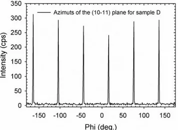
Fig. 2 Phi-scan curve of asymmetric GaN (101¯1) reflection plane for
sample D. Every peak shows the azimuths of the (101¯1) plane. The diffractive peak repeats every 60°
An in-plane Φ-scan was also taken by rotating the sam- ple around its surface-normal direction in order to investi- gate the in-plane alignment of GaN film. Figure 2 shows the Φ-scan pattern of the (10 1¯1) plane of sample D. It can be seen in Fig. 2 that the diffraction peaks from the (10 1¯1) plane of GaN were observed at 60° intervals, which clearly confirms the good single crystal hexagonal structure of the GaN epilayer.
The influence of the nitridation time on the structural properties of a GaN epilayer
Heteroepitaxial thin films with a large lattice-mismatch with respect to the substrate in turn form a mosaic structure of slightly misoriented sub-grains [18, 19, 22], which is char- acterized by the nucleation of slightly misoriented islands
of the crystallographic orientations [18, 23].
The parameters of the vertical and lateral coherence length and tilt angle can be obtained from the Williamson– Hall measurement, and the twist angle from an approach, which was developed by Srikant et al. [23] or from di- rect measurement [24], which explains the superposed ef- fect of the tilt and twist on the broadening of the full-widths at half-maximum (FWHMs) of the off-axis plane rocking curves [25].
Each contribution to the broadening of the particular XRD curves can be separated in the Williamson–Hall mea- surement [18, 25]. Specifically, in triple-axis diffractome- ter measurements, the broadening of the rocking curve (angular-scan or ω-scan) of the symmetric (0002), (0004), and (0006) reflections for the GaN epitaxial layer is influ- enced only by the tilt angle αtilt and short coherence length parallel to the substrate surface L.
Separation analogous of the tilt angle αtilt and short co- herence length can be made with the Williamson–Hall plot, when βΩ (sin θ )/λ is plotted against (sin θ )/λ for each re-
flection and fitted by a straight line. Then, the tilt angle αtilt is obtained from the slope of the linear dependence, and lat- eral coherence length L(L = 0.9/(2y0)) from the inverse of the y-intersection y0 of the fitted line with the ordinate, where βΩ is the FWHM in angular unit, θ is the Bragg re-
flection angle, and λ is the X-ray wavelength.
In the radial-scan direction (ω 2θ -scan) of the sym- metric reflections (0002), (0004), and (0006), a small ver- tical correlation length and a heterogeneous strain along the
c-axis causes a broadening of the Bragg reflections. This
two parameters L⊥ and ε⊥ can similarly be derived from the Williamson–Hall plot. The L⊥ and ε⊥ parameters can be derived from the β2θ−Ω (cos θ )/λ against (sin θ )/λ plots for each reflection.
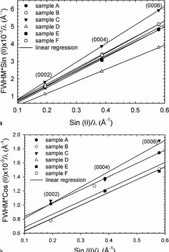
Figure 3 shows the corresponding Williamson–Hall plots for reflections (0002), (0004), and (0006) for the triple-axis (a) ω-scan and (b) ω 2θ of all the samples with different nitridation times. The straight lines are linear fits of the ex- perimental data. The expected linear behavior of the graphs and the coalescence of these islands towards a smooth sur- face. The mosaic structure of the epilayers is determined by the size and angular distribution of the mosaic blocks. The vertical and lateral correlation lengths, heterogeneous strain, and degree of mosaicity as expressed by the tilt and twist angles are important parameters in characterizing the qual- ity of the epitaxial films with a large lattice mismatch to the substrate [17, 19, 22]. The mosaic blocks are assumed to be slightly misoriented with respect to each other. The out- of-plane rotation of the blocks perpendicular to the surface normal is the mosaic tilt, and the in-plane rotation around the surface normal is the mosaic twist. The average absolute values of tilt and twist are directly related to the full width at half maximum (FWHM) of the corresponding distributions
×
− =
× ×
Fig. 3 Williamson–Hall plot for the GaN layers without nitrida-
tion and with different nitridation times. (a) Triple-axis ω scan and (b) triple-axis ω 2θ scan were measured for the (000l) (l 2, 4, 6) reflections indicated in the figure. The lines result from a linear fit of the data
is experimentally well confirmed, which gives rather accu- rate tilt angle values.
The lateral coherence lengths and tilt angles are shown in Fig. 4. As can be seen, the tilt angles for all the samples were rather small. It can be seen in the figure that, as the ni- tridation times increased, the tilt angles decreased first and then increased to 10.6 10−3 degrees for sample C (60 s). From these nitridation times, we can see small increments in the tilt angle. The minimum tilt angle was obtained for sample D. The lateral coherence lengths were determined to range from 182 to 467 nm. As seen in Fig. 4, as the nitri- dation times increased the L increased first and then de- creased. The maximum values were observed for the nitri- dation times of 10 s (sample B).
The vertical coherence lengths L values are shown in Fig. 5. Its values range from 60 to 100 nm. It can be seen in Fig. 5 that there is an increment in all the samples except for sample D.
Fig. 5 Vertical coherence length and heterogeneous strain obtained
from the Williamson–Hall plot as a function of the nitridation time
The strain normal to the substrate ε⊥ values, which was obtained for all the samples, is shown in Fig. 5. The ε⊥ val- ues range from 4.2 10−4 to 5.5 10−4. Small changes were observed for a heterogeneous strain with the nitrida- tion time length.
The mean twist angle between the subgrains can be ex- trapolated from a fit to the measured double-axis scans data for different (hkl) reflections in the skew symmetric diffrac- tion. Several extrapolation methods have been reported in the literature for the mean twist angle calculation [18, 23,
26]. However, all of these methods include a complicated calculation and fitting procedure for the extraction of the twist angle from the experimental data. On the other hand, Zheng et al. [24] proposed a simple empirical approach to obtain the mean twist angle directly without falling into complications.
The FWHM of the rocking curve of an imperfect film is composed of several contributions, such as the mean tilt, twist, the average size of sub-grains, and inhomogeneous strain distributions. Although the broadening, which is due to a limited domain size and an inhomogeneous strain, can
Fig. 4 Tilt and lateral coherence length obtained from the
The influence of nitridation time on the structural properties of GaN grown on Si (111) substrate 77
− 3
3
=
1
Fig. 6 FWHM values of the rocking curves of Φ and ω scans for (hkl)
reflections (marked in the figure) vary with the inclination angle χ for all of the samples. FWHMs of Φ scan increase with the increment of
χ angle, while those of ω scan decrease. The lines are a guide for the
eyes
be significant in highly imperfect films, their effects have been eliminated by the use of a slit of 0.6 mm placed in front of the detector in double-axis ω-scans. Indeed, their contri- bution to the overall broadening was found to be of minor influence in this measurement case.
In addition, the (0002) reflection and (hkl) reflections with h or k non-zero orientation of our samples with triple- axis ω 2θ -scans both exhibit a small FWHM. The last important point is that the intrinsic width of the reflection for the crystal and the apparatus broadening for all the ex- perimental reflections are negligible because these effects amount to only a few arcsec. For this reason, we can only measure the broadening that is caused by the twist by using (hkl) reflections in the skew geometry.
The extended FWHMs of ω and Φ-scans that were ob- tained by using the fit of the Pseudo-Voigt function to the rocking curves are shown in Fig. 6 as a function of increas- ing χ for all the samples. It can be seen in Fig. 6 that the FWHMs of ω and Φ-scans are nearly the same when the in- clination angle is 78.6°. In this inclination angle, the (123¯1) reflection appears. These results showed that the rocking- curve widths of ω or Φ scans for this higher χ angle are close to the twist angles. In every respect, the FWHMs of
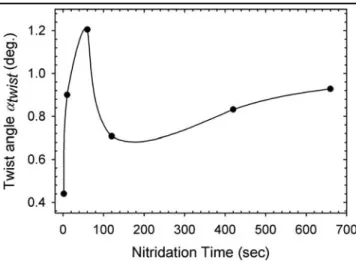
Fig. 7 The dependence of the twist angle on the nitridation time
sample C (with 60 s nitridation) and then decreases to 0.7° for sample D (with 120 s nitridation) nitridated the longest. Based on this observation, it can be argued that the mean twist angle of the GaN epilayers that are grown on Si sub- strate is strongly affected by the time elapsed for the nitrida- tion of the substrate before intiating GaN growth.
There are three main types of dislocations present in GaN thin film that are grown on Si (111) with two steps [7–16, 18, 24, 27]: the pure edge dislocation with Burgers vector b = 1 (112¯0) ((a)), the pure screw dislocation with Burgers vector b = (0001) ((c)), and the mixed disloca- tion with b = 1 (112¯3) ((c + a)). The coherence lengths, and the twist and tilt are correlated with the different types of dislocations. As reported by Metzger et al. [18], for (0002)-oriented GaN epitaxial films, the mean twist an- gle is monotonically related to the density of edge-type of the threading dislocation (TD) with Burgers vector b = 1/3(112¯0), while the mean tilt angle is monotonically re- lated to, and can be converted into, the density of the screw- type of TD with Burgers vector b = (0001). Thus, in the present study, all the existing dislocation lines were treated as the types defined by Metzger et al. [18].
The screw dislocation (b = (0001)) density (Dscrew) can be calculated from the equation [28, 29],
α2
Φ-scans are larger than those of the χ -scans with the change Dscrew = tilt
2 , (1)
of the inclination angle χ . Therefore, the mean twist an- gles must be the average value of the FWHMs of the ω and
Φ-scans of χ 78.6°.
The measured mean twist angle of the GaN layers is shown in Fig. 7 as a function of the nitridation time. The mean twist angle is strongly dependent on the nitridation time. The minimum mean twist angle value was obtained as 0.4° for sample A (without nitridation). It increases with the nitridation time and reaches to a maximum value of 1.2° for
4.35|bscrew|
where αtilt is the tilt angle, and b is the Burgers vector length (bscrew= 0.5185 nm).
The edge type dislocations with Burgers vector (b = 3 (112¯0)) reconcile an azimuthal rotation of crystallites around the surface normal. From the measured twist angle
αtwist, an edge-type dislocation density can be calculated. If dislocations are piled up in small angle grain boundaries,
=
[ ] [ ]
( ) ( )
Fig. 8 The edge, screw, and total dislocation density as a function of
the nitridation time
the edge dislocation density (Dedge), therefore, can be cal- culated according to [28, 29],
αφ
Dedge =
2.1|bedge|L
, (2)
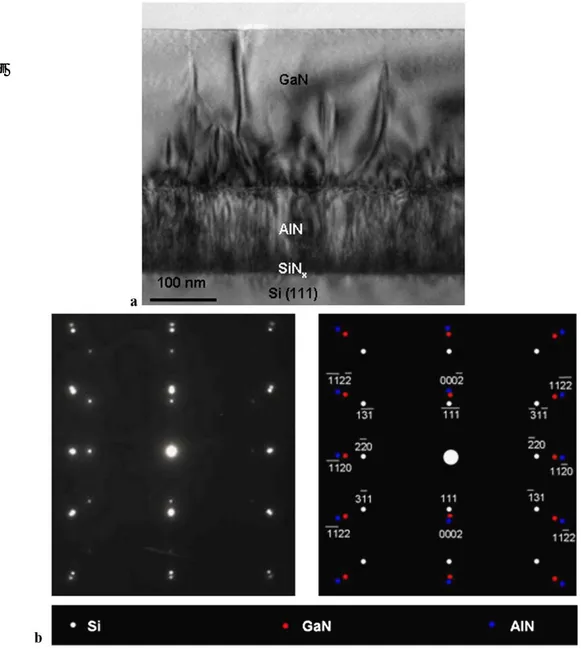
where b is the Burgers vector length (bedge 0.3189 nm). Figure 8 shows the edge, screw, and total dislocation den- sity as a function of nitridation time length. As can be seen from this figure, the edge and screw dislocation densities are approximately equal to each other for sample A (with- out nitridation). The edge dislocation density changed with the nitridation times. On the other hand, the screw disloca- tion densities approximately keep constant for all the nitri- dation times. These results show that the nitridation process is much more effective on the edge type dislocation density. The microstructure of the grown layers was revealed by TEM. The cross-sectional and plan-view TEM specimens were prepared from the grown layers. In Fig. 9(a), we show the cross-sectional TEM images of the GaN films grown on Si (111) with a 660 s nitridated buffer layer (sample F). The GaN-AlN and Si were viewed in the 11¯00 and 112¯ pro- jections, respectively. A relatively rough interface between the HT-AlN nucleation layer and GaN, and a high density of threading dislocations (TD) can be clearly observed. From Fig. 9(a), it can be seen that, the dislocation density de- creases rapidly within 50 nm from the AlN/GaN interface into the GaN layer. Since dislocations cannot end within a crystal, that is, the ends of a dislocation can only be at free surfaces, or at interfaces, the apparent change in the dis- location density within the GaN layer requires an explana- tion. The dislocations originating from the GaN/AlN inter- face may change direction and bend back to the interface that they originate from. Tilt or twist boundaries that are said to exist within the GaN layer may also assist in such changes in dislocation directions. Some studies even sug- gest the presence of small angle grain boundaries with the
lationships were determined for GaN-AlN on Si (111) by taking the selected area electron diffraction (SAED) pat- terns in TEM (Fig. 9(b) and Fig. 10(b), (c)). It is notewor- thy that despite the presence of an amorphous SiNx inter-
layer, the selected area electron diffraction (SAED) con- firms the well-known orientation relationships between GaN (AlN) and Si [34], which are (112¯0)GaN // (112¯0)AlN // (11¯0)Si,(11¯00)GaN // (11¯00)AlN // (112¯)Si, and (0001)GaN // 0001 AlN // 111 Si. By this, it has also been proven that GaN and AlN have hexagonal crystal structures and are sin- gle crystals.
Several reports have addressed the issue of a crystallo- graphic relationship between AlN and Si despite the amor- phous SiNx between them. One of the suggestions was that
the amorphous SiNx layer has some short range order that
necessitates the orientation of the AlN layer in this fash- ion [34]. According to some others, there exists in the SiNx
a top layer of a few atomic distances that is crystalline [36]. According to Dobos et al. [37], Nakada et al. [36], and Kaiser et al. [34], the epitaxial relationship is transferred from Si into AlN and GaN through the amorphous SiNx
layer by the presence of crystalline regions, Si3N4 inclu- sions, or holes in the SiNx layer. Other explanations include
the short-range tetrahedral coordination that was maintained in the SiNx layer [34, 41, 42], and the nucleation and growth of GaN islands from intrinsic or extrinsic defects by a “pin- hole model” [40].
In our view, perhaps the most plausible explanation is that the amorphous SiNx layer is not continuous and that there
must be some points of actual contact between the crys- talline Si substrate and deposited AlN layer [40]. It is then conceivable to assume that such locations of contact would inevitably behave like seeds in bulk single crystal growth techniques in turn leading to an overall crystallographic re- lationship between AlN and Si despite the presence of an intermittent amorphous SiNx . If such a mode of deposition
is operational, then the large lattice mismatch between AlN and Si in the locations of true contact could also act as a source for dislocation emissions, and thereby explain the GaN layer [18]. The wavy nature of the AlN/GaN interface may also be related to the tilt and twist boundaries in the GaN layer.
Other aspects requiring explanation are the crystallo- graphic relationship between the AlN layer and Si substrate, as well as the apparent stress that consequently also leads to the observed high dislocation density within the AlN layer. If the interface was truly between the AlN and Si substrate, the crystallographic relationship and relatively high disloca- tion density, originating from the interface due to the large lattice mismatch between the two crystals, would provide a straightforward explanation. However, the AlN/Si interface has been shown, in the present study and others, to contain an amorphous SiNx layer [34, 36, 37]. The orientation re-
The influence of nitridation time on the structural properties of GaN grown on Si (111) substrate 79
high dislocation density within AlN. Our observations on the cross sections taken from different locations of the same sample showed that SiNx is indeed intermittent. It may fur-
ther be suggested that the tilt and twist boundaries that are said to exist in GaN may also be related to the growth modes of the AlN layer.
In addition to the arguments mentioned above, the crystal orientation of the hexagonal AlN with the basal planes paral- lel to its interface with the substrate may also arise from the simple thermodynamic requirement of lowering the surface energy. As a thin film and, therefore, having its largest sur- faces parallel to the substrate it should be expected that AlN with a hexagonal crystal structure would, unless otherwise dictated by a crystalline substrate, prefer to form outer sur- faces out of densely packed, i.e., low energy, basal planes. Therefore, even if no effect was imposed by the amorphous SiNx for a particular orientation relationship, a free-growing
AlN layer would be expected to position itself in the ob- served fashion, i.e., basal planes parallel to the substrate.
A plain AlN film on Si contains a large number of dis- locations due to the strain relaxation of the film [30]. Foll- staedt et al. [31] and Datta et al. [32] have demonstrated that, plan-view TEM imaging is generally accepted as a more trustworthy method for TD density measurement, compared to other techniques, such as atomic force microscopy (AFM) and cathodoluminescence (CL). These techniques cannot be used effectively to detect a-type edge dislocations that thread to the film surface, since such dislocations do not create steps on the surface that are detectable by AFM, and are probably not effective nonradiative recombination centers that are detectable by CL [31–34].
The threading dislocations (TD) density of sample F (with 660 s nitridation) was determined by plan-view TEM. The plan-view image of sample F is shown in Fig. 10(a). All
Fig. 9 (a) Cross-sectional
Bright Field TEM image, and (b) corresponding diffraction zone axis and Si [112¯] zone axis pattern for GaN-AlN [11¯00]
∼
×
[ ]
[ ]
∼
Fig. 10 (a) Plan-view TEM micrographs of the GaN layer on the AlN
nucleation overlayer grown with the insertion of an SiNx layer (sam- ple F) and (b) corresponding diffraction pattern, and (c) indexed sketch of the basic reflections for the GaN [0001] zone axis
of the images were bright-field (BF) images which were col- lected by using multi-beam diffraction conditions. The plan- view specimens were investigated in the 0001 zone-axis orientation, which were nearly in the optical axis. The deter- mined values are characteristic for the near surface region, only ( top 100 nm). Moreover, the crystal defects, which were revealed by cross-sectional studies, did not propagate to the surface, and are not visible in the plan-view im- ages [30, 34, 35].
As shown in Fig. 10(a), a network structure of defect ar- rays was also observed. The image shows that the disloca- tions in the epitaxial layers are not uniformly distributed. In order to determine the TD densities, the number of TDs was counted for approximately 10 different plan-view TEM images similar to those shown in Fig. 10. All of the images, for TD density determination, were collected with their GaN 0001 zone axis. The density of these threading dislocations was approximately 9 109 cm−2, which is comparable to the values that were calculated with the HR-XRD measure- ments.
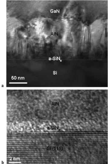
Fig. 11 (a) Low-magnification and (b) HRTEM image of the Si/AlN
interface with the a-SiNx intermediate layer
Between the Si substrate and AlN layer, a thin layer ( 2 nm) was observed (Fig. 11). From the cross-sectional High Resolution TEM (HRTEM) image (Fig. 11(b)) for sample F it is observed that this thin layer is amorphous SiNx (a-SiNx ). This a-SiNx is also observed in several
Si/AlN systems [33, 34, 36–42].
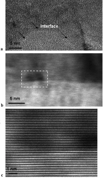
Cross-sectional HRTEM images are shown for the GaN/AlN interface in Fig. 12. A rough interface is observed mostly for the GaN/AlN layers (Fig. 11(a) and Fig. 12(a)). However, smoother interface segments were also observed in some regions (Fig. 12(b), (c)).
From the SAED results, with the epitaxial relation, it can be observed that the crystal orientation of Si (111) seems to be transferred mostly through the amorphous SiNx into the
AlN and GaN layers. One reason could be the short-range tetrahedral coordination of each atom, which is obviously continued in the SiNx layer. Another explanation could be
small crystalline SiN or Si3N4 within the interlayer, which transfer the orientation relation [34, 36]. Secondly, a locally, thicker SiNx layer in the structures can cause the interrup-
The influence of nitridation time on the structural properties of GaN grown on Si (111) substrate 81
× and the interface structure of AlN/SiNx /Si (111) and dislo-
cation densities (edge and screw types) were investigated by both TEM and XRD measurements of the hexagonal epi- taxial GaN films grown on Si (111). The nitridation time lengths ranged from 0 to 660 s. The mosaic structure of the GaN layers was affected by the nitridation time length. We obtained the largest values for vertical and lateral coherence length at 10 s nitridation. On the other hand, when the Si (111) was not nitridated, the smallest twist angle was ob- tained (sample A). The smallest tilt angle of a 6.9 10−3 degree was obtained for the 120 s nitridated sample. From the dislocation measurements, we can see that the edge type dislocation densities are much more affected from the nitri- dation process. However, screw dislocation densities are less affected by nitridation. From the SAED results, with the epi- taxial relation, it can be observed that the crystal orientation of Si (111) seems to be transferred mostly through the amor- phous SiNx into the AlN and GaN layers. However, it is im-
portant to avoid an excessively large SiNx layer thickness,
which would totally interrupt the transfer of the epilayer re- lation from the Si (111) substrate to the epitaxial and would cause the polycrystalline deposition of GaN.
Acknowledgement This work is supported by the European Union
under the projects EU-METAMORPHOSE, EU-PHOREMOST, EU- PHOME, and EU-ECONAM, and TUBITAK under Project Numbers 105E066, 105A005, 106E198, 106A017, and 107A012. One of the au- thors (E.O.) also acknowledges partial support from the Turkish Acad- emy of Sciences.
References
Fig. 12 (a) HRTEM image of the rough AlN/GaN interface shown
by the arrows, (b) HRTEM image of the smoother AlN/GaN interface region, and (c) magnified view of the selected region of (b)
tion of the crystal symmetry transfer. For this reason, we obtained (0002) orientated AlN grains (Fig. 9) with slightly tilted grains. In our present study, it was important to avoid an excessively large SiNx layer thickness that would totally
interrupt the transfer of the epilayer relation from the Si (111) substrate to the epitaxial layer and that would cause a polycrystalline deposition of GaN, as given by other growth process [13–16, 31, 33–35].
4 Conclusions
In the present study, the influence of in-situ substrate nitrida- tion time (assumed to cause an SiNx amorphous interlayer)
on the characteristics of the structural features by HXRD,
1. S.N. Mohammad, A. Salvador, H. Morkoç, Proc. IEEE 83, 1420 (1996)
2. L. Shen, S. Heikman, B. Moran, R. Coffie, N.-Q. Zhang, D. But- tari, I.P. Smorchkova, S. Keller, S.P. DenBaars, U.K. Mishra, IEEE Electron Device Lett. 22, 457 (2001)
3. S. Butun, M. Gokkavas, H. Yu, E. Ozbay, Appl. Phys. Lett. 89, 073503 (2006)
4. T. Tut, M. Gokkavas, B. Butun, S. Butun, E. Ulker, E. Ozbay, Appl. Phys. Lett. 89, 183524 (2006)
5. H. Yu, D. Caliskan, E. Ozbay, J. Appl. Phys. 100, 033501 (2006) 6. R. Gaska, J.W. Yang, A. Osinsky, Q. Chen, M. Asif Khan, A.O.
Orlov, G.L. Snider, M.S. Shur, Appl. Phys. Lett. 72, 707 (1998) 7. A. Dadgar, C. Hums, A. Diez, J. Bläsing, A. Krost, J. Cryst.
Growth 297, 279 (2006)
8. S. Pal, C. Jacob, Bull. Mater. Sci. 27, 501 (2004) 9. A. Krost, A. Dadgar, Mater. Sci. Eng. B 93, 77 (2002) 10. M.-H. Kim, Y.-G. Do, H.C. Kang, D.Y. Noh, S.-J. Park, Appl.
Phys. Lett. 79, 2713 (2001)
11. Z.L. Fang, S.P. Li, J.C. Li, H.Z. Sun, S.J. Wang, J.Y. Kang, Thin Solid Films 516, 6344 (2008)
12. K. Cheng, M. Leys, S. Degroote, B. Van Daele, S. Boeykens, J. Derluyn, M. Germain, G. Van Tendeloo, J. Engelen, G. Borghs, J. Electron. Mater. 35, 592 (2006)
13. S. Raghavan, J.M. Redwing, J. Appl. Phys. 98, 023514 (2005) 14. J. Huang, Z. Ye, L. Wang, J. Yuan, B. Zhao, H. Lu, Solid-State
15. W.-Y. Uena, Z.-Y. Li, S.-M. Lan, S.-M. Liao, J. Cryst. Growth 280, 335 (2005)
16. C.-L. Wu, J.-C. Wang, M.-H. Chan, T.T. Chen, S. Gwo, Appl. Phys. Lett. 83, 4530 (2003)
17. P.R. Hageman, S. Haffouz, V. Kirilyuk, A. Grzegorczyk, P.K. Larsen, Phys. Stat. Sol. (a) 188, 523 (2001)
18. T. Metzger, R. Höppler, E. Born, O. Ambacher, M. Stutzmann, R. Stömmer, M. Schuster, H. Göbel, S. Christiansen, M. Albrecht, H.P. Strunk, Philos. Mag. A 77, 1013 (1998)
19. B. Heying, X.H. Wu, S. Keller, Y. Li, D. Kapolnek, B.P. Keller, S.P. DenBaars, J.S. Speck, Appl. Phys. Lett. 68, 643 (1995) 20. M.E. Vickers, M.J. Kappers, R. Datta, C. McAleese, T.M. Smee-
ton, F.D.G. Rayment, C.J. Humphreys, J. Phys. D Appl. Phys. 38, 99 (2005)
21. N.G. Weimann, L.F. Eastman, J. Appl. Phys. 83, 3656 (1998) 22. V. Holy, J. Kubena, E. Abramof, K. Lischka, A. Pesek, E. Kop-
pensteiner, J. Appl. Phys. 74, 1736 (1993)
23. V. Srikant, J.S. Speck, D.R. Clarke, J. Appl. Phys. 82, 4286 (1997) 24. X.H. Zheng, H. Chen, Z.B. Yan, Y.J. Han, H.B. Yu, D.S. Li, Q.
Huang, J.M. Zhou, J. Cryst. Growth 255, 63–67 (2003) 25. G.K. Williamson, W.H. Hall, Acta Metall. 1, 22 (1953) 26. Y.J. Sun, O. Brandt, K.H. Ploog, J. Mater. Res. 18, 1247 (2003) 27. H. Sasaki, S. Kato, T. Matsuda, Y. Sato, M. Iwami, S. Yoshida,
J. Cryst. Growth 298, 305 (2007)
28. P. Gay, P.B. Hirsch, A. Kelly, Acta Metall. 1, 315 (1953) 29. C.G. Dunn, E.F. Koch, Acta Metall. 5, 548 (1957)
30. H. Lahreche, P. Vennegues, B. Beaumont, P. Gibart, J. Cryst. Growth 205, 245 (1999)
31. D.M. Follstaedt, P.P. Provencio, N.A. Missert, C.C. Mitchell, D.D. Koleske, A.A. Allerman, C.I.H. Ashby, Appl. Phys. Lett. 81, 2758 (2002)
32. R. Datta, M.J. Kappers, J.S. Barnard, C.J. Humphreys, Appl. Phys. Lett. 85, 3411 (2004)
33. X. Weng, S. Raghavan, J.D. Acord, A. Jain, E.C. Dickey, J.M. Redwing, J. Cryst. Growth 300, 217 (2007)
34. S. Kaiser, M. Jakob, J. Zweck, W. Gebhardt, O. Ambacher, R. Dimitrov, A.T. Schremer, J.A. Smart, J.R. Shealy, J. Vac. Sci. Technol. B 18(2), 733 (2000)
35. F. Wu, S. Zamir, B. Meyler, J. Salzman, Y. Golan, J. Electron. Mater. 31, 88 (2002)
36. Y. Nakada, I. Aksenov, H. Okumura, Appl Phys Lett. 73, 6951 (1998)
37. L. Dobos, B. Pécz, E. Feltin, B. Beaumont, P. Gibart, Vacuum 71, 285 (2003)
38. M.-H. Kim, Y.-C. Bang, N.-M. Park, C.-J. Choi, T.-Y. Seong, S.-J. Park, Appl. Phys. Lett. 78, 2858 (2001)
39. A. Chakraborty, K.C. Kim, F. Wu, J.S. Speck, S.P. DenBaars, U.K. Mishra, Appl. Phys. Lett. 89, 041903 (2006)
40. M. Tamura, M. López-López, T. Yodo, Superficies Vacío 13, 80 (2001)
41. Z. Fang, Surf. Coat. Technol. 202, 4198 (2008)
42. Z.L. Fang, J.Y. Kang, W.J. Huang, H.T. Sun, M. Lu, J.F. Kong, W.Z. Shen, J. Phys. Chem.C 112, 4925 (2008)