Contents lists available atScienceDirect
Ceramics International
journal homepage:www.elsevier.com/locate/ceramint
Room temperature deposition of XRD-amorphous TiO
2
thin
films:
Investigation of device performance as a function of temperature
Maria Luisa Grilli
a, Mehmet Yilmaz
b,c,⁎, Sakir Aydogan
c,d,⁎, Burcu Bozkurt Cirak
eaENEA-Italian National Agency for New Technologies, Energy and Sustainable Economic Development, Energy Technology Department, Casaccia Research Centre, Via
Anguillarese 301, 00123 Roma, Italy
bDepartment of Science Teaching, Faculty of K. K. Education, Atatürk University, 25240 Erzurum, Turkey
cAdvanced Materials Research Laboratory, Department of Nanoscience and Nanoengineering, Graduate School of Natural and Applied Sciences, Ataturk University, 25240
Erzurum, Turkey
dDepartment of Elect. & Elect. Engn., Faculty of Engineering, Ardahan University, 75000 Ardahan, Turkey eDepartment of Alternative Energy Sources, Vocational High School, Erzincan University, 24000 Erzincan, Turkey
A R T I C L E I N F O Keywords: TiO2 Films Electrical properties A B S T R A C T
In this study, TiO2thinfilms were fabricated by radio frequency sputtering at room temperature in pure Ar
atmosphere starting from a 6 in. TiO2target. The thickness of thefilms was controlled by deposition time and the
effect of Ar sputtering pressure on the characteristics of TiO2thinfilms was evaluated. Surface morphology and
optical properties of TiO2films were investigated using X-ray diffraction (XRD), Atomic Force Microscopy
(AFM), Scanning Electron Microscopy (SEM) and UV–Vis spectrophotometry. Also, the refractive index and extinction coefficient of films were inferred by fitting spectrophotometric data. Schottky diode were fabricated by evaporation of Ni on TiO2films. Current-voltage (I-V) measurements of Ni/TiO2films showed that the
rec-tifying properties of the device improves with the increasing of TiO2film density and thickness. Therefore, the
best I-V characteristic of the device was investigated depending on the temperature. Also, Ni/n-TiO2/p-Si/Al
devices were fabricated to understand their transport mechanism.
1. Introduction
TiO2(titanium dioxide) is receiving increasing attention due to its
remarkable properties such as high transparency in the visible region, wide and direct bandgap, abundance in nature, absence of toxicity and good chemical stability in adverse environment, etc.[1,2]. TiO2occurs
in three phases: rutile, anatase and brookite. Among these, only anatase and rutile phases crystallize in the tetragonal system and both have great technological interest. Rutile is the most stable structure of TiO2
[3]and it is more easily formed as a single crystal form. TiO2is a native
n-type semiconductor having a wide bandgap of 3.2 eV for anatase[4] and 3.0 eV for rutile. In TiO2 semiconductor, the conduction band is
mainly made up of Ti 3d states for both anatase and rutile phases, and Ti valence states are highly localized, so the formation of native n-type defects generates electrons to the Ti lattice. These properties make TiO2
a good candidate for various applications from catalysis to sensors[5]. Additionally, due to its high refractive index, TiO2may be used in solar
cell applications as well as in optoelectronic and memory devices. Due
to the above mentioned properties, numerous efforts have been made to fully understand TiO2's characteristics and to tailor its performances for
the requested applications. For example, Patel et al.[6]have studied Cu/TiO2/FTO device and have reported that its responsivity value is
0.897 A/W and detectivity value is 4.5 × 10¹²Jones. Also, Konenkamp
and Rieck[7]focused on the electrical properties of nano-porous TiO2
films and they found the ideality factor as 1.7 eV for Pt/TiO2Schottky
diode. In the literature, several techniques such as spray pyrolysis[8], sol-gel spin coating [9], pulsed laser deposition [10]and sputtering [11]are used to fabricate TiO2thinfilms. Synthesizing good quality
films at low temperature is important for device applications. Because of this, and because of its high versatility and industrial scalability sputtering steps forward among the above mentioned thinfilm growth techniques. In addition, it has other important advantages such as the possibility to obtain high quality and uniform coatings, good adhesion betweenfilm and substrate, etc.[12].
In this study, the electrical properties of Schottky devices fabricated with amorphous TiO2 thin films grown by Radio Frequency (RF)
https://doi.org/10.1016/j.ceramint.2018.03.222
Received 29 January 2018; Received in revised form 22 March 2018; Accepted 25 March 2018
⁎Corresponding authors at: Advanced Materials Research Laboratory, Department of Nanoscience and Nanoengineering, Graduate School of Natural and Applied Sciences, Ataturk
University, 25240 Erzurum, Turkey.
E-mail addresses:[email protected](M.L. Grilli),[email protected],[email protected](M. Yilmaz), [email protected],[email protected](S. Aydogan),[email protected](B.B. Cirak).
Available online 27 March 2018
0272-8842/ © 2018 Elsevier Ltd and Techna Group S.r.l. All rights reserved.
sputtering technique at different sputtering pressures were investigated. TiO2films were grown at room temperature in pure Ar atmosphere.
Oxygen gas was not intentionally added during the growth to achieve non stoichiometric and conductivefilms. The structural, morphological, optical and electrical properties of TiO2films grown at high and low
sputtering pressures were evaluated by XRD (X-ray diffraction), AFM (Atomic Force Microscope), SEM (Scanning Electron Microscope), UV–Vis spectrophotometric and Schottky measurements.
2. Experimental
TiO2thinfilms were grown on fused silica and p-type Si substrates.
Si wafer had 1–10 Ωcm resistivity, 270 µm thickness and (100) or-ientation. The growth procedures were carried out by RF sputtering in Ar atmosphere starting from a 6-in. diameter TiO2target of 99.99%
purity. The distance between target and substrate was adjusted to 70 mm. Base pressure in the sputtering chamber was about 2 × 10⁻⁴ Pa. Also, the power of RF source and substrate temperature were 250 W and 300 K, respectively. The thickness of thefilms was determined by surface profilometer KLA-Tencor P-10 and inferred by fitting trans-mittance and reflectance data measured by a Lambda 950 spectro-photometer. To analyze Schottky characteristics of the films, Ni con-tacts each of 7.85 × 10⁻³ cm2 area and 70 nm thickness, were
deposited on TiO2films using DC magnetron sputtering at 10−5Torr.
Also, a thin Al layer of 80 nm thickness was evaporated on the back side of the Si substrate as the ohmic contact. So, Ni/n-TiO2/p-Si/Al devices
were obtained. The energy-band diagram of the Ni/n-TiO2/p-Si device,
that enables to get information about the nature of junction barrier or interface, which are the key parameters to estimate the electrical con-duction mechanism of device under equilibrium conditions, is shown in Fig. 1.
Deposition conditions (RF power, substrate temperature, target to substrate distance, deposition time) for sputtered TiO2films were fixed,
except for the Ar sputtering pressure which was chosen as 0.36 and 0.90 Pa, as the low and high sputtering pressure, respectively. Growth at different Ar pressures resulted in films with different morphology and different thickness (103 and 84 nm, respectively).
The electrical properties of Ni/n-TiO2/p-Si/Al devices were
in-vestigated as a function of TiO2film by using current-voltage (I-V) and
the capacitance-voltage (C-V) measurements. The I-V curve of the best device was then measured as a function of the temperature.
3. Results and discussion
Fig. 2. reports the XRD patterns of amorphous TiO2films deposited
at different sputtering pressures. These graphs clearly show that both films have an amorphous phase, probably due to the low energy of the growth process, which was conducted at low temperature and relatively low RF power. In addition, higher is the sputtering pressure during the deposition, lower is the energy of the process. AFM and SEM analyses showed that TiO2films have nanostructured crystalline network with
nanometric grain size. Presence of short range crystalline order in XRD-amorphousfilms was found also by other authors[13–17].Fig. 3shows the surface morphology of TiO2films. Both films present a granular
morphology andfilm uniformity increases with a reduction of porosity, as observed in the film with higher thickness grown at the lower sputtering pressure. Thisfilm shows also an increased grain size and a lower surface roughness. Grain agglomerations on thefilm surface can be a possible reason for this, and line scan AFM measurements, showing an increasing particles height, support this idea. RMS roughness de-creases from 0.83 nm to 0.48 nm in 84 and 103 nmfilms, grown at high and low sputtering pressure respectively. The grain structure and the lack of atomically smooth terraces suggest that allfilms have XRD-amorphous/polycrystalline nature. Similar results were reported by Mosquera et al.[18]for pulsed cathodic arc TiO2films.
The optical properties offilms have considerable interest for op-toelectronic applications. From the optical transmittance curve we can get information about electronic structure of the materials. Transmittance (T) and reflectance (R) curves of RF sputtered TiO2films
in the wavelength range of 250–1400 nm are presented inFig. 4. All films are transparent in the visible region and exhibit sharp fall in transmittance in the UV region corresponding to the absorption edge. In TiO2, electronic transition from valence band to conduction band
oc-curs between O 2p (valence band edge) and Ti 3d (t2 g) (conduction
band edge). Therefore, the optical band gap edge is attributed to direct interband transition [19]. The energy band gap of thinfilms can be calculated by transmittance and reflectance data. The absorption coefficient (α) for a film of thickness (d) can be obtained by the fol-lowing expression[20]: ⎜ ⎟ = ⎛ ⎝ − ⎞ ⎠ α dln R T 1 (1 )2 (1) From the Tauc's method, we can separate three regions in the Fig. 1. The energy-band diagram of the Ni/n-TiO2/p-Si heterojunction structure
under equilibrium conditions.
absorption edge spectrum for amorphous semiconductors: i) the weak absorption edge which depends on defects and impurities, ii) the ex-ponential edge region which originates from the structural randomness of the system and iii) the high absorption region which is associated with the optical energy gap [21]. In the high absorption region, the parabolic relation between absorption coefficient and the energy of incident photon energy (hυ) can be applied for a direct band gap semiconductor[22]:
= −
αhν A(hν E )g1/2 (2)
where A is the characteristic parameter related to the electron-hole mobility, hv is the photon energy and Eg is the optical band gap. The optical band gap values of TiO2 films can be determined by
extra-polating the linear portion of the curve to the energy axis, as shown in
Fig. 5. The Eg values are determined as 3.92 and 3.84 eV for 84 nm and 103 nm thick TiO2films, respectively. These values are in good
agree-ment with those reported for TiO2films obtained by different
techni-ques[23,24].
The band gap narrowing observed in the sample grown at lower sputtering pressure can be related to the higher number of carriers due to point defects in the crystal structure. To identify the relationship between the structural disorder and the optical band gap, the tail of the absorption coefficient near the onset band gap is considered as an ex-ponential function of photon energy, called Urbach energy (Eu)[25]:
=
αhυ α e0 hυEu (3)
whereαhυis related to the absorption profile obtained experimentally and α0 is a constant. The Urbach values of thefilms were calculated from reciprocal slope of lnα vs.hυ plot given as inset inFig. 5. According Fig. 3. SEM and AFM images of TiO2films a) 84 nm b) 103 nm.
Fig. 4. Transmittance and reflectance curves of TiO2films.
Fig. 5. The plot of (αhν)2vs. (hν) and ln(α) vs. hν (inset figure) of TiO 2films.
to Mott and Davis[26], the calculated Eu values should be in the range of 0.046 and 0.66 eV for amorphous semiconductors. Our results de-monstrate an increasing tendency of the Urbach energy with the in-creasing offilm thickness, which support the possibility of short range order, locally occurring due to the formation of a weak crystalline phase [27]. Also, increase in the band tails width leads to the reduction of the optical band gap. The dispersion of refractive index n and the extinction coefficient k, obtained by fitting spectrophotometric data is reported in Fig. 6.
It can be clearly seen fromFig. 6that the refractive index (n) de-creases with increasing wavelength in the visible region, which is characteristic of the normal dispersion. Additionally, the refractive index (n) values are higher for the sample grown at the lower sputtering pressure, probably due to its higher density. Extinction coefficient (k) has a reverse behavior, indicating lower absorption for the thicker and more crystallinefilm. The variation of ε1(real part) andε2(imaginary
part) with photon energy can be calculated by following Eqs.[28–30]
= −
ε1 n2 k2 (6)
=
ε2 2nk (7)
Fig. 7depicts the photon energy dependence of the dielectric con-stants of TiO2thinfilms with different film thickness. These results are
in harmony with literature data[31,32]. The loss tangent (tanδ given in Fig. 7) identifies how electromagnetic absorption occurs in the mate-rial. The angleδ may be defined as the phase difference between the applied electricfiled and the induced current. According toFig. 7, tanδ
values increase withfilm thickness. Sharp increase is also observed in the range of 3.2 eV and 4 eV. Similar results were observed also for ZnO thinfilms[33].
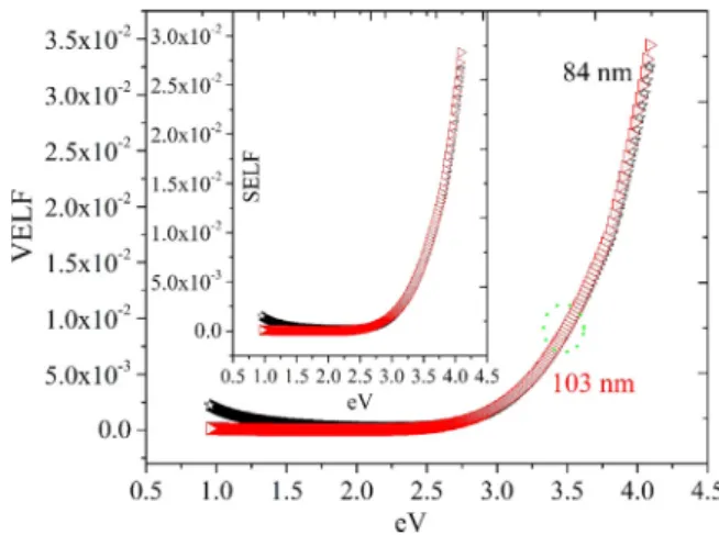
The volume energy loss function (VELF) and surface energy loss function (SELF) indicate energy loss of electrons travelling the bulk and surface of the material, respectively. They can be estimated by using the following formula[33,34]: = + V ε ε ε ELF img reel2 img2 . (8) = + + S ε ε ε ( 1) ELF img reel 2 img2 . (9)
Fig. 8shows the variation of volume energy loss function (VELF) and surface energy loss function (SELF) with wavelength. FromFig. 8it can be observed that either volume and surface energy loss functions have higher value at lower wavelength (higher photon energy). Also, the VELF and SELF exhibit similar behavior with the variation of en-ergy, even though energy loss of the free charge carriers moving across the bulk material is higher than that of electrons moving across the surface. This means that the energy loss occurring in the interior of the grownfilms is associated to interband electronic transitions[33–35]. Fig. 8 shows also that no distinct bands associated with interband transitions are observed in the visible photon energies. Similar results were observed by Kermedi et al.[34]. According to refs.[35,36], the value of SELF and VELF can be written as follows, taking energy (hυ) into consideration: = hυ Volume ne ε m ( ) * 2 0 (10) = hυ Surface ne ε m ( ) 1 2 * 2 0 (11)
where n is the electron density and the m* is the effective electron mass. These relations also indicate that the ratio of VELF/SELF is 2=1.41. FromFig. 8, VELF/SELF ratio calculated at approximately 3.52 eV (see Fig. 8green circular data) is9.6 10 /6.9 10× −3 × −3=1.39,which is close to 1.41. This confirms that higher energy losses occur when free charge carriers move throughout the material compared to the surface.
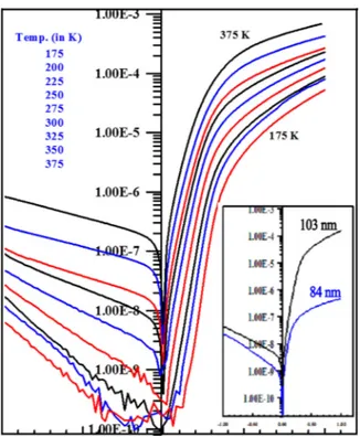
Fig. 9 shows the temperature dependent current-voltage (I–V) curves of the Ni/TiO2Schottky barrier diode fabricated with the 103 nm
TiO2thickfilm (film grown at lower sputtering pressure). Furthermore,
room temperature I-V curves of both devices having 84 nm and 103 nm thick TiO2films are reported as inset for comparison. The device
fab-ricated with TiO2 film grown at the lower sputtering pressure gives
better rectifying behavior, because of its better surface morphology and Fig. 6. The extinction coefficient and refractive index variation with
wave-length of TiO2films.
Fig. 7. The spectral dispersion of dielectric constants.
Fig. 8. Plot of wavelength dependence of VELF and SELF for TiO2thinfilms.
(For interpretation of the references to color in thisfigure, the reader is referred to the web version of this article.)
its higher density. As can be seen from the characteristics, both reverse and forward bias currents increase with increasing temperature. Espe-cially, the bias dependence of the reverse currents toward low tem-perature is clear and this indicates that the Ni/TiO2Schottky barrier
diode shows non-ideal behavior.
Temperature and voltage-dependent reverse-bias current-voltage characteristics are reported inFig. 10. The reverse bias currents give information about barrier height of Schottky diodes. The reverse bias currents do not depend on the bias for ideal Schottky diodes. As seen in Fig. 10, the Schottky barrier height on TiO2strongly depends on the
reverse bias and the dependence of the reverse current from bias be-comes more evident at the lower temperatures. This behavior is one of the non-ideal Schottky barrier height properties.
To obtain the current-voltage (I-V) characteristics of Schottky diodes on moderately doped semiconductors, it is accepted that the thermionic emission (TE) is the main current transport mechanism and I is given as[37]: = ⎡ ⎣ ⎢ ⎛⎝ ⎞ ⎠− ⎤⎦⎥ I I qV nkT ( ) exp0 1 , (12) where the pre-factorIois the reverse current for zero bias:
= ⎛ ⎝− ⎞ ⎠ I AA T qΦ kT ( * )exp , o 2 b (13) where A is the effective diode area, A* is the Richardson constant of TiO2(671 A/cm2K2), T is the absolute temperature,Φbis the effective
barrier height for V bias, q is the electron charge, k is the Boltzmann constant and n is the ideality factor, which is determined from the slope of the forward I-V characteristics through Eq.(14):
=
n q
kT[d /dln( )]V I (14)
Furthermore, n reflects how the diode obeys to thermionic emission mechanism, being n = 1 for an ideal diode. The ideality factor n can be determined from the slope of the I–V characteristics on a semiloga-rithmic plot. The main reasons of the non-ideal situation may be the presence of the defects generation in the depletion layer of the semi-conductor, the recombination of carriers in the surface states, the tun-neling mechanism between states in the band-gap of semiconductor, the high injection of carriers at high bias and the parasitic IRsdrop due to
series resistance Rs. The barrier height of a Schottky diode is
de-termined as: =
eΦb kTln(AA T I* 2/ )0 (15)
The analysis of the current-voltage (I-V) characteristics of the Schottky barrier diodes at room temperature may, however, not give detailed information about conduction process of these devices and the nature ofΦb. Therefore, it may be useful to obtain wide temperature
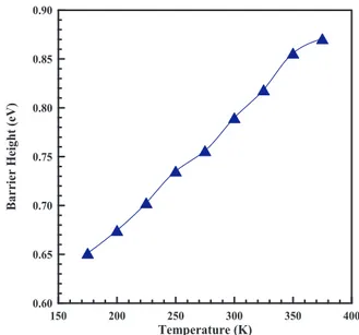
range measurements of I-V characteristic since the conduction me-chanism of the devices is governed by a thermal process. The tem-perature T dependent of ideality factor n and the barrier heightΦb
curve for the Ni/TiO2Schottky barrier diode are shown inFig. 11. From
Fig. 9. The I-V plots of the Ni/TiO2Schottky barrier diode as a function of
temperature. Inset: comparison of RT I-V plots for devices fabricated with 103 nm and 84 nm thick TiO2films.
Fig. 10. Temperature and voltage-dependent reverse-bias current-voltage characteristics of the Ni/TiO2(103 nm) Schottky barrier diode.
Fig. 11. The temperature T dependent- ideality factor and barrier height curves of Ni/TiO2Schottky barrier diode.
the experimental results both ideality factor and the barrier height were found strongly temperature dependent, such that the ideality factor values changed from 1.53 (375 K) to 1.93 (175 K), while the barrier height values varied from 0.87 eV (375 K) to 0.48 eV (175 K). The higher ideality factor can be attributed to the presence of a thick in-terfacial insulator layer between the Ni and TiO2semiconductor[37].
Moreover, the presence of the TiO2thin layer between Ni and Si, and
imperfections on TiO2surface may be the reason of the higher ideality
factors and of the high reverse current values[38].
Above∼225 K, the value of ideality factors n increased slightly with increasing temperature T such that the correlation has been deviated. Since the ideality factor reflects the quality of interface of the junction devices, re-distribution of the interface states and generation/re-combination current in the depletion region of TiO2may cause
non-correlation between n and T. Furthermore, the presence of the traps or the defects at the Ni/TiO2interface may also allow tunneling-assisted
emission processes instead of pure thermionic emission conduction mechanism and this may lead to a little increase of n with increasing T [39]. Norde's method [40] can be used to determine the series re-sistance and the barrier height of a Schottky diode. For this purpose, the following F(V) function has been derived in the modified Norde's method: = − ⎛ ⎝ ⎞ ⎠ F V V kT q I V AA T ( ) 2 ln ( ) * 2 (16)
F(V)–V curves are given inFig. 12, where the value of F(V) corre-sponding to the minimum (F(V0)) satisfies the relationship,
= + − Φ F V V kT q ( ) 2 b 0 0 (17) where V0is the corresponding voltage.Fig. 12depicts also the F(V)–V
curve of the Ni/TiO2 Schottky barrier device as a function of
tem-perature. Furthermore, the value of the series resistance RShas been
obtained from Norde's method by using:
= −
Rs kT γ n
qI
( )
(18) (γis an integer higher than n).
From modified Norde's method, the experimental barrier values changed from 0.59 eV (175 K) to 0.87 eV (375 K), as shown inFig. 13. The series resistance RSof a Schottky barrier diode may be
con-sidered for higher forward biases/currents to take into account power losses. The temperature dependence of the series resistance RSof our
Ni/TiO2Schottky barrier diode is shown in Fig. 14. In general, the
values of the series resistance decrease with increasing temperature because of an increase in the number of thermally generated carriers in the Ni/TiO2. The calculated series resistance values range from 635Ω at
375–14 kΩ at 175 K.
By taking into account the series resistance Rs, Eq.(12)becomes:
= ⎡ ⎣ − ⎤ ⎦ I I q V IR nkT exp ( s) , 0 (19) Once the necessary arrangements are performed, Eq.(19)may be written as shown in Eq.(20), and Rsvalues may be obtained. We can
determine the Rs values for all temperatures also using Cheung's
method, as shown in Eq.(21) [41].
Fig. 12. F(V)–V plots of the Ni/TiO2Schottky barrier device as a function of
temperature.
Fig. 13. T-Φbplot of the Ni/TiO2Schottky barrier diode obtained from the
modified Norde's model.
Fig. 14. The temperature dependence of the series resistance RSof Ni/TiO2
= + dV d I nkT q IR (ln ) s (20) ⎜ ⎟ = − ⎛ ⎝ ⎞ ⎠ ⎛ ⎝ ⎞ ⎠ H I V nkT q I AA T ( ) ln * 2 (21)
H I( )may be written also as follows:
= +
H I( ) nΦb IRs, (22)
The plots of dV
d(ln )I vs.I and H I( ) vs.I yield the linear curves, and
slopes of both curves correspond toRsvalues. A plot ofd(ln )dVI vs. I can be
drawn by using Eq.(20)and it should be linear. Thus, Rs and n values can be determined from the slope and y-axis intercept indicatingnkT
q of
in this plot, respectively. Also, the barrier heights are obtained from Eq. (22)using y-axis intercept too.
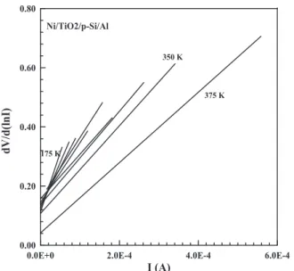
Figs. 15 and 16depict the plots of experimental dV/dln(I) and H(I) versus I for Ni/n-TiO2/p-Si/Al devices as a function of temperature.
Table 1shows main junction parameters of Ni/n-TiO2/p-Si/Al devices
calculated from Cheung's function. It is clearly seen that all parameters depend on temperature: n and Rs values decrease, whileΦb values
increase with increasing of temperature. These variations are expected for non-ideal junction devices since several current conduction me-chanisms may occur in such devices, apart from the pure thermionic emission mechanism[37,42]. The reason of this behavior may be the inhomogeneity properties of the barrier height or the interface and the presence of titanium dioxide layer. The number of electrons which cross a higher barrier increases with temperature [43]. Furthermore, the response of the device parameters to the temperature follows Norde's function.
Capacitance-voltage (C-V) measurement for Schottky diodes is a very powerful tool to gain information about these devices. In these measurements, an AC signal is superimposed to the DC bias.Fig. 17 depicts the forward and the reverse bias C–V plots of the Ni/TiO2
Schottky barrier diode measured at various frequencies at room tem-perature. As seen, when the high-frequency (especially at 1000 kHz) of C is weakly voltage-independent, as long as the free carrier relaxation time is short with respect to the AC frequency, the response of the pacitance originates from the depletion edge. The higher values of ca-pacitance at 100 kHz and 200 kHz are due to the excess caca-pacitance resulting from the interface states in equilibrium with the TiO2that can
response to the AC signal. Namely, the interface states at lower fre-quencies (100 kHz and 200 kHz) follow the AC signal, whereas at higher frequencies they cannot follow the alternating current signal.
Furthermore, the C-V measurements were carried out as a function of temperature at f = 500 kHz frequency, and results are reported in Fig. 18. At forward bias, the capacitance increased with increasing temperature due to the presence of the oxygen defects which may cause Fig. 15. Plots of dV/dlnI versus I for the Ni/TiO2/p-Si/Al diode as a function of
temperature.
Fig. 16. Plots of H(I) versus I for the Ni/TiO2/p-Si/Al diode as a function of
temperature.
Table 1
Main junction parameters of Ni/n-TiO2/p-Si/Al devices calculated from
Cheung's functions.
Temperature (K) dV/d(lnI) H(I)-I
n Rs(Ω) Φb(eV) Rs(Ω) 175 7.42 4019 0.43 4022 200 7.22 3094 0.48 3112 225 6.91 2555 0.53 2558 250 6.68 2023 0.58 2040 275 6.61 1507 0.61 1498 300 6.02 1073 0.67 1078 325 4.88 1577 0.72 1567 350 3.54 1484 0.78 1489 375 1.28 1089 0.82 1011
Fig. 17. The forward and the reverse bias C–V plots of the Ni/TiO2Schottky
a drop in the capacitance at low temperatures. Namely, the temperature dependence of the capacitance is due to a freeze out of electrons on the deep centers in the band gap of TiO2[44,45].
4. Conclusion
Non stoichiometric TiO2thinfilms were deposited on Si and fused
silica substrates by RF sputtering technique at room temperature and different Ar sputtering pressures. The structural, morphological, optical and electrical features of thefilms were correlated to film morphology. Optical band gap and Urbach energy values were determined and correlated to free charge concentration in different TiO2 films.
Experimental I-V measurements showed that the I-V characteristic of the device improved for the TiO2film grown at lower sputtering
pres-sure, which has a more homogenous and a denser surface morphology. Thus, the temperature dependence of (I-V) measurement was conducted for suchfilm. Results indicated that both ideality factor and the barrier height are strongly dependent on temperature, such that the ideality factor values changed from 1.53 (375 K) to 1.93 (175 K), while the barrier height values varied from 0.87 eV (375 K) to 0.48 eV (175 K). Moreover, the series resistance affected adversely the Schottky diode, decreasing with increasing temperature due to an increase in the number of thermally generated carriers. Additionally, the temperature dependence of C-V measurements showed that capacitance increased with increasing temperature due to the presence of oxygen defects which might cause a drop in the capacitance at low temperatures. References
[1] M.L. Grilli, A. Sytchkova, M.R. Mancini, F. Zurlo, G. Hu, E. Di Bartolomeo, A. Piegari, Optical and electrical properties of TiO2 based transparent conductivefilms and multilayer systems fabricated by radio frequency sputtering and E-beam eva-poration, IET Conference Publications, (CP704), 2016.
[2] H. Ogawa, T. Higuchi, A. Nakamura, S. Tokita, D. Miyazaki, T. Hattori, T. Tsukamoto, Growth of TiO2thinfilm by reactive RF magnetron sputtering using oxygen radical, J. Alloy. Compd. 449 (1) (2008) 375–378.
[3] J. Haines, J.M. Leger, X-ray diffraction study of TiO2up to 49 GPa, Phys. B: Condens. Matter 192 (3) (1993) 233–237.
[4] S. Chatterjee, Titania–germanium nanocomposite as a photovoltaic material, Sol. Energy 82 (2) (2008) 95–99.
[5] B. Toubal, R. Bensaha, F. Yakuphanoglu, The influence of copper-cobalt co-doping on optical and electrical properties of nanostructures TiO2thinfilms prepared by sol-gel, J. Sol-Gel Sci. Technol. 82 (2) (2017) 478–489.
[6] D.B. Patel, K.R. Chauhan, W.H. Park, H.S. Kim, J. Kim, J.H. Yun, Tunable TiO2films for high-performing transparent Schottky photodetector, Mater. Sci. Semicond. Process. 61 (2017) 45–49.
[7] R. Könenkamp, I. Rieck, Electrical properties of Schottky diodes on nano-porous TiO2films, Mater. Sci. Eng.: B 69 (2000) 519–521.
[8] I. Oja, A. Mere, M. Krunks, C.H. Solterbeck, M. Es-Souni, Properties of TiO2films prepared by the spray pyrolysis method, Solid State Phenom. 99 (2004) 259–264. [9] Z. Wang, U. Helmersson, P.O. Käll, Optical properties of anatase TiO2thinfilms
prepared by aqueous sol–gel process at low temperature, Thin Solid Films 405 (1) (2002) 50–54.
[10] S. Yamamoto, T. Sumita, A. Miyashita, H. Naramoto, Preparation of epitaxial TiO2 films by pulsed laser deposition technique, Thin Solid Films 401 (1) (2001) 88–93. [11] A. Dakka, J. Lafait, M. Abd-Lefdil, C. Sella, Optical study of titanium dioxide thin
films prepared by RF sputtering, MJ Condens. Matter 2 (1) (1999) 153–156. [12] T. Narushima, K. Ueda, T. Goto, H. Masumoto, T. Katsube, H. Kawamura, Y. Iguchi,
Preparation of calcium phosphatefilms by radiofrequency magnetron sputtering, Mater. Trans. 46 (10) (2005) 2246–2252.
[13] Z. Zhao, B.K. Tay, G. Yu, Room-temperature deposition of amorphous titanium dioxide thinfilm with high refractive index by a filtered cathodic vacuum arc technique, Appl. Opt. 43 (6) (2004) 1281–1285.
[14] V. Tiron, I.L. Velicu, M. Dobromir, A. Demeter, F. Samoila, C. Ursu, L. Sirghi, Reactive multi-pulse HiPIMS deposition of oxygen-deficient TiOxthinfilms, Thin Solid Films 603 (2016) 255–261.
[15] P.B. Nair, V.B. Justinvictor, G.P. Daniel, K. Joy, P.V. Thomas, Influence of film thickness and annealing atmosphere on the structural, optical and luminescence properties of nanocrystalline TiO2thinfilms prepared by RF magnetron sputtering, J. Mater. Sci.: Mater. Electron. 24 (7) (2013) 2453–2460.
[16] H. Fukuda, Rapid Thermal Processing for Future Semiconductor Devices, Elsevier, U.S.A, 2003, p. 87.
[17] S. Çörekçí, K. Kizilkaya, T. Asar, M.K. Öztürk, M. Çak-Mak, S. Ozgelik, Effects of thermal annealing andfilm thickness on the structural and morphological proper-ties of titanium dioxidefilms, Acta Phys. Pol.-Ser. A Gen. Phys. 121 (1) (2012) 247–248.
[18] A.A. Mosquera, J.M. Albella, V. Navarro, D. Bhattacharyya, J.L. Endrino, Effect of silver on the phase transition and wettability of titanium oxidefilms, Sci. Rep. 6 (2016) 32171.
[19] Y.R. Park, K.J. Kim, Structural and optical properties of rutile and anatase TiO2thin films: effects of Co doping, Thin Solid Films 484 (1) (2005) 34–38.
[20] K. Kara, E.S. Tüzemen, R. Esen, Annealing effects of ZnO thin films on p-Si (100) substrate deposited by PFCVAD, Turk. J. Phys. 38 (2) (2014) 238–244. [21] A.E.B. Alwany, O.M. Samir, M.A. Algradee, M.M. Hafith, M.A. Abdel-Rahim,
Investigation of the effect of film thickness and heat treatment on the optical properties of TeSeSn thinfilms, World J. Condens. Matter Phys. 5 (3) (2015) 220. [22] M. Yilmaz, Characteristic properties of spin coated ZnO thinfilms: the effect of Ni
doping, Phys. Scr. 89 (9) (2014) 095802.
[23] K. Bouabid, A. Ihlal, Y. Amira, A. Sdaq, A. Assabbane, Y. Ait-Ichou, G. Nouet, Optical study of TiO2thinfilms prepared by sol-gel, Ferroelectrics 372 (1) (2008) 69–75.
[24] S. Yin, Y. Inoue, S. Uchida, Y. Fujishiro, T. Sato, Crystallization of titania in liquid media and photochemical properties of crystallized titania, J. Mater. Res. 13 (4) (1998) 844–847.
[25] S. Ilican, M. Caglar, Y. Caglar, Sn doping effects on the electro-optical properties of sol gel derived transparent ZnOfilms, Appl. Surf. Sci. 256 (23) (2010) 7204–7210. [26] N. Mott, E. Davis, Electronic Process in Non-Crystalline Materials, 2nd ed.,
Clarendon Press, Oxford, 1979.
[27] I. Sta, M. Jlassi, M. Hajji, M.F. Boujmil, R. Jerbi, M. Kandyla, H. Ezzaouia, Structural and optical properties of TiO2thinfilms prepared by spin coating, J. Sol-Gel Sci. Technol. 72 (2) (2014) 421–427.
[28] H.A. Mohamed, Some physical properties of ZnO thinfilms prepared by thermal oxidation of metallic Zn, Optoelectron. Adv. Mater.-Rapid Commun. 6 (3–4) (2012) 389–393.
[29] S. Chander, A. Purohit, C. Lal, M.S. Dhaka, Enhancement of optical and structural properties of vacuum evaporated CdTe thinfilms, Mater. Chem. Phys. 185 (2017) 202–209.
[30] S. Sönmezoǧlu, B. Erdoǧan, İ. Askeroǧlu, Investigation of optical, structural and morphological properties of nanostructured boron doped TiO2thinfilms, Bull. Mater. Sci. 36 (7) (2013) 1239–1245.
[31] A.S. Gadallah, M.M. El-Nahass, Structural, optical constants and photoluminescence of ZnO thinfilms grown by Sol-Gel spin coating, Adv. Condens. Matter Phys. 2013 (2013),http://dx.doi.org/10.1155/2013/234546.
[32] M.A. El-Raheem, A.M. Al-Baradi, Optical properties of as-deposited TiO2thinfilms prepared by DC sputtering technique, Int. J. Phys. Sci. 8 (31) (2013) 1570–1580. [33] A.I. Ali, A.H. Ammar, A.A. Moez, Influence of substrate temperature on structural,
optical properties and dielectric results of nano-ZnO thinfilms prepared by Radio Frequency technique, Superlattices Microstruct. 65 (2014) 285–298.
[34] S. Kermadi, N. Agoudjil, S. Sali, L. Zougar, M. Boumaour, L. Broch, F. Placido, Microstructure and optical dispersion characterization of nanocomposite sol–gel TiO2–SiO2thinfilms with different compositions, Spectrochim. Acta Part A: Mol. Biomol. Spectrosc. 145 (2015) 145–154.
[35] M.M. El-Nahass, H.S. Soliman, A. El-Denglawey, Absorption edge shift, optical conductivity, and energy loss function of nano thermal-evaporated N-type anatase TiO2films, Appl. Phys. A 122 (8) (2016) 775.
[36] F. Schmithüsen, M. De Boissieu, M. Boudard, J. Chevrier, F. Comin, Electron energy loss spectroscopy investigation of volume and surface plasmons at the Al–Pd–Mn fivefold surface, Mater. Sci. Eng.: A 294 (2000) 867–870.
[37] E.H. Roderick, R.H. Williams, Metal–Semiconductor Contacts, Clarendon Press, Oxford, 1998.
[38] S. Zeyrek,Ş. Altındal, H. Yüzer, M.M. Bülbül, Current transport mechanism in Al/ Si3N4/p-Si (MIS) Schottky barrier diodes at low temperatures, Appl. Surf. Sci. 252
Fig. 18. The experimental C-V measurements of the Ni/TiO2Schottky barrier
(8) (2006) 2999–3010.
[39] K. Ejderha, A. Zengin, I. Orak, B. Tasyurek, T. Kilinc, A. Turut, Dependence of characteristic diode parameters on sample temperature in Ni/epitaxy n-Si contacts, Mater. Sci. Semicond. Process. 14 (1) (2011) 5–12.
[40] A. Kocyigit, I. Orak, Z. Çaldıran, A. Turut, Current–voltage characteristics of Au/ ZnO/n-Si device in a wide range temperature, J. Mater. Sci.: Mater. Electron. 28 (22) (2017) 17177–17184.
[41] S.K. Cheung, N.W. Cheung, Extraction of Schottky diode parameters from forward current‐voltage characteristics, Appl. Phys. Lett. 49 (2) (1986) 85–87.
[42] A.A.M. Farag, I.S. Yahia, Rectification and barrier height inhomogeneous in
Rhodamine B based organic Schottky diode, Synth. Met. 161 (1–2) (2011) 32–39. [43] R.T. Tung, Electron transport of inhomogeneous Schottky barriers, Appl. Phys. Lett.
58 (24) (1991) 2821–2823.
[44] S. Aydoğan, M. Sağlam, A. Türüt, Effect of temperature on the capacitance–-frequency and conductance–voltage characteristics of polyaniline/p-Si/Al MIS de-vice at high frequencies, Microelectron. Reliab. 52 (7) (2012) 1362–1366. [45] B.P. Lakshmi, M.S.P. Reddy, A.A. Kumar, V.R. Reddy, Electrical transport properties
of Au/SiO2/n-GaN MIS structure in a wide temperature range, Curr. Appl. Phys. 12 (3) (2012) 765–772.