Atomic strings of group IV, III–V, and II–VI elements
S. Tongay, E. Durgun, and S. Ciraci
Citation: Appl. Phys. Lett. 85, 6179 (2004); doi: 10.1063/1.1839647 View online: http://dx.doi.org/10.1063/1.1839647
View Table of Contents: http://aip.scitation.org/toc/apl/85/25
Atomic strings of group IV, III–V, and II–VI elements
S. Tongay, E. Durgun, and S. Ciracia)
Department of Physics, Bilkent University, Ankara 06800, Turkey
(Received 12 April 2004; accepted 25 October 2004)
A systematic first-principles study of atomic strings made by group IV, III–V, and II–VI elements has revealed interesting mechanical, electronic, and transport properties. The double bond structure underlies their unusual properties. We found that linear chain of C, Si, Ge, SiGe, GaAs, InSb, and CdTe are stable and good conductor, although their parent diamond (zincblende) crystals are covalent(polar) semiconductors but, compounds SiC, BN, AlP, and ZnSe are semiconductors. First row elements do not form zigzag structures. © 2004 American Institute of Physics.
[DOI: 10.1063/1.1839647]
Active research on metal nanowires has been driven by their strange atomic structures and unusual physical properties.1 Their theoretically predicted string, as well as single or multishell tubular structures2,3stepwise variation of electronic conductance with the cross section and giant Young’s modulus have been revealed experimentally.4–6 Technologically, the problem of interconnects between nan-odevices is still a real challenge and awaiting for the control-lable synthesis of nanowires which can make good contacts. In contrast to metal nanowires, carbon nanotubes, and carbon strings7–11which have been thoroughly investigated, there is not much known about atomic chains made by group IV(Si, Ge, Sn), group III–V (BN, AlP, GaAs, Insb, etc.) and group II–VI(ZnSe, CdTe, etc.) elements.7–10In the current trend of miniaturization of electronic devices there has been a grow-ing interest in stability and conductivity of the atomic wires of these elements which make well-known 3D covalent or polar semiconductor crystals leading to important optoelec-tronic applications.11,12 In this letter, we performed first-principles pseudopotential plane wave calculation usingVASP
software13within generalized gradient approximation14to re-veal geometric, electronic, and transport properties of atomic strings made by group IV, III–V, and II–VI elements. While efforts have been intensified to synthesize, stable carbon-chains15,16and silicon chains,17present results are ex-pected to bring about a new perspective to the applied re-seach on molecular electronics.18
All structures are treated by supercell geometry includ-ing several atoms, and all atomic positions and lattice param-eters are optimized by minimizing total energy and atomic forces. Depending upon the ultrasoft pseudopotential of the elements,13 the kinetic energy cutoffs 300 eV⬍ប2关k + G兴2/共2m兲⬍340 eV have been used. Brillouin zone of the
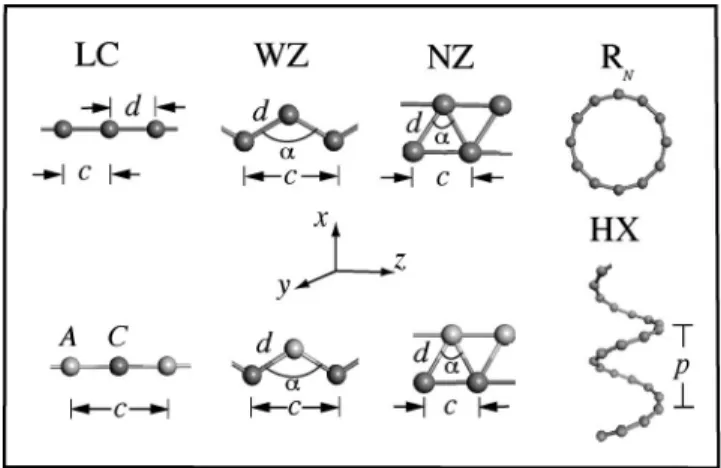
smallest supercell is sampled by 61 special k-points, while the number of k-points of the larger supercell is scaled ac-cording to the size of the cell. A thorough analysis of stabil-ity has been performed by reoptimizing atomic structure af-ter displacing atoms from their original optimized positions. Furthermore, ab initio molecular dynamics calculations car-ried out at 800 K for large number of time steps to check whether the string structures remain stable at high tempera-ture. We considered various string structures, such as linear chain(LC), narrow angle (NZ), and wide angle (WZ) planar
zigzag, helix(HX), and ring (RN, N being number of atoms
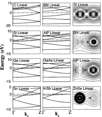
in the ring) structures. These structures and their character-istic parameters are shown in Fig. 1. Table I summarizes our results for bonding, electronic, and geometric structure of various strings obtained from our calculations. The electronic band structure and total charge density contour plots of se-lected LC structures are shown in Fig. 2
The LC is a stable structure for all elemental and com-pound strings studied in this work. The binding energy per atom for group IV elements (per basis for group III–V and II–VI compounds) is close to bulk binding (cohesive) energy. High binding energies despite only two nearest neighbors of each atom is due to the double bond(one, -bond by s + pz valance orbitals and two, -bond by px,y valance orbitals).
The double-bonding pattern is reflected in mechanical prop-erties of these linear structures. For example, the elastic stiff-ness defined by=兩d2E / d2⑀兩
⑀=0(i.e., second derivative of the
strain energy per basis with respect to axial strain) is calcu-lated to be 32 and 100 eV for Si-LC and AlP-LC, respec-tively. Interestingly, single-wall carbon nanotubes have in the range of 50– 60 eV. The double bond is covalent in the strings made by group IV elements, but it gains some polar character due to the charge transfer from group III(II) ele-ment to group V(VI) element in the compound strings. The polarity of the bonds is expected to bring about additional constraints in the atomic and electronic structure. The char-acter of the bonds is displayed in Fig. 2 using charge density
a)Electronic mail: [email protected]
FIG. 1. Description of linear chain(LC), planar narrow angle zigzag (NZ) and wide angle zigzag(WZ), helix (HX), ring 共RN兲 structures. c: lattice
parameter; d: bond length;␣: apex angle; p: pitch length; C: cation; A: anion.
APPLIED PHYSICS LETTERS VOLUME 85, NUMBER 25 20 DECEMBER 2004
contour plots. The covalent character of the bonds of C, Si, and Ge linear chains is depicted by the symmetry of contour lines and also by the bond charge at the center of the bond. However, in compound LCs, such as BN and GaAs, the charge distribution becomes asymmetric, and bond-charge shifts towards anion. This situation is reminiscent of those found in bulk crystals, but the distribution of charge exhibits differences.
The double bond formation is essential not only for high binding energy, but also for electronic structure and ballistic conductance. In C–LC, the doubly degenerate band crosses the Fermi level at kz=/ 2c and becomes half filled.
This situation gives rise to Peierls distortion in C–LC.10 Whereas Si, Ge, and Sn–LC behave differently; in addition to doubly degenerate-band,*-band dips below the Fermi level near the zone edge. This way the double bond is
slightly delocalized and accordingly the cohesive energy is relatively lowered. Consequently, Peierls’ dimerization can-not occur in Si–, Ge–, Sn–LC structures. Three bands cross-ing the Fermi level also refute similar dimerization in metal-lic compounds given in Table I.
Planar NZ and WZ zigzag structures are derived from string and their apex angle ␣ have been calculated to be ⬃60° and ⬃120°, respectively. Because of equilateral tri-angle structure of NZ, each atom forms four bonds. Previ-ously it was found that metal atoms, such as Al, Au, etc. form these LC, WZ, and NZ structures.19 They appear as local minima on the Born–Oppenheimer surface with LC having lowest but NZ highest binding energy. In the present, study we found the same trend for the string structures of Si, Ge, Sn, and SiGe, whereby the binding energy of NZ is ⬃20% higher than that of LC; WZ has an intermediate value. In contrast to III–V row elements, C, BN, and SiC make neither stable WZ nor NZ structure, inspite of the fact that both structures lead to positive binding energy. This situation can be explained by the relatively shorter bond distance of C, BN, and SiC, which leads to stronger ionic repulsion in closed structures. For the compound strings of the third and higher row elements, WZ occurs with binding energy rela-tively higher than that of LC; but NZs become unstable and are transformed to other exotic structures. Strong repulsive force between two anions or two cations in the nearest neigh-bor distance of NZ structure is the prime cause of instability. On the other hand, HX and RNstructures are stable for C and
BN, but are not formed by the rest of the elements and com-pounds in Table I. In BN, HX and RNare polygons where flat
edges are made by BN basis, where B atoms are placed at the corners of polygon. The C-ring structure exhibits bond alter-nation and bond angle alteralter-nation depending on the number of carbon atoms N forming the ring.8
We note that LC of C, Si, Ge, Sn, GeSi, GaAs, InSb, and CdTe are metallic, but BN, SiC, AlP, and ZnSe are semicon-ductor. As a prototype band structure, first and second lowest valence bands of BN–LC are nondegenerate and are derived from 2s and 2pzvalence orbitals of nitrogen. The third band
is doubly degenerate and has 2px,yorbital character. The first conduction band is derived mainly from boron orbitals. The indirect band gap, Eg= 4 eV for BN, 1.6 eV for AlP, but di-minishes for GaAs and InSb.
TABLE I. Summary of calculated binding energy, electronic structure, bond length of atomic strings. First entry: binding energy Eb in eV/atom or eV/basis. Second entry: metal M with conductance Go= 2e2/ h or
insulator I with energy gap Egin eV. Third entry: bond length d in Å. Last column is the calculated bulk
cohesive energies in eV.
LC WZ NZ Bulk C 8.5; M : 2G0; 1.3 — — 9.1 Si 3.4; M : 3G0; 2.2 3.9; M : 2G0; 2.2 4.1; M : 4G0; 2.7 5.4 Ge 3.0; M : 3G0; 2.3 3.6; M : 2G0; 2.3 3.9; M : 4G0; 2.5 4.5 Sn 2.5; M : 3G0; 2.7 2.9; M : 2G0; 2.7 3.0; M : 4G0; 2.9 3.8 SiC 11.3; I : 2.1 eV; 1.6 — — 15.2 GeSi 6.3; M : 3G0; 2.2 7.5; M : 2G0; 2.2 8.2; M : 4G0; 2.5 10.0 BN 16.2; I : 4 eV; 1.3 — — 17.5
AlP 7.0; I : 1.6 eV; 2.1 7.6; I : 0.9 eV; 2.2 — 10.4 GaAs 5.5; M : 3G0; 2.3 6.3; I : 0.2 eV; 2.2 — 8.3
InSb 4.5; M : 3G0; 2.8 5.0; M : 3G0; 2.8 — 6.9
ZnSe 4.1; I : 0.7 eV; 2.2 4.7; I : 0.8 eV; 2.2 — 6.1 CdTe 2.9; M : 1G0; 2.6 3.5; I : 1.5 eV; 2.7 — 4.9
FIG. 2. Calculated energy band structure of LC structures made by C, BN, Si, AlP, Ge, GaAs, Sn, and Insb. For the sake of comparison bands of Si, Ge, and Sn are presented in double cell. Zero of energy is set at Fermi level, EF.
Contour plots of the total charge density of Si, BN, AlP, and ZnSe, on a plane passing through the bond.
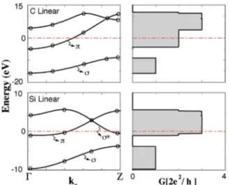
The analysis of quantum ballistic conductance of a finite string between two electrodes, is crucial for the metallic con-nection of devices in nanoelectronics. However, this requires the detailed knowledge of the contacts. Here, we consider only the quantum ballistic conductance of infinite C–LC and Si–LC by using Green’s function method within orthogonal empirical tight-binding method and Landauer formula G = 2e2/ hT (T is the transmission function to be obtained from
the trace of retarded and advanced Green’s functions and coupling functions20). Since the character of the bonds in LC is different from bulk bonds, the energy parameters obtained from bulk diamond and silicon crystals are not transferable. Then we first fit the energy parameters to the first-principles bands calculated in this study. In Fig. 3, we illustrate the tight-binding bands and the ballistic conductance of perfect infinite linear chain of C and Si calculated using tight-binding Green’s functions method. We see that for very small bias voltage Si–LC is better conductor than C–LC, and both Si and C are better conductor than Au–LC having conduc-tance only G = G0. We note that the number of band states at
a given energyN determines the ballistic conductance G of a
perfect, infinite nanowire, since each of these band crossing states yields a current transporting state with unit transmis-sion function共T=1兲. As a result the conductance at a given energy is G =NG0.
In conclusion, we showed that stable string structures made by individual group IV or group III–V and II–VI ele-ments can be formed. The double bond pattern underlies un-usual physical properties, such as high elastic stiffness, co-hesive energy and quantum conductance higher than Au and Cu atomic chains. In general, the conductance of metallic (band gap of semiconducting) strings increases (decreases) with increasing row number of elements in the periodic table. The polarity of the bonds increases with increasing valency difference of elements forming the compound. First row elements display different behavior; while they form stable linear chain, helix, and ring structures, they lead to instabilities in zigzag structures.
1
For a recent review of the subject, S. Ciraci, A. Buldum, and I. P. Batra, J. Phys.: Condens. Matter 13, R537(2001).
2
H. Mehrez and S. Ciraci, Phys. Rev. B 56, 12632(1997).
3
O. Gülseren, F. Ercolessi, and E. Tosatti, Phys. Rev. Lett. 80, 3775(1998). 4
H. Ohnishi, Y. Kondo, and K. Takayanagi, Nature(London) 395, 780
(1998). 5
N. Agraït, J. G. Rodrigo, and S. Vieira, Phys. Rev. B 47, 12345(1993); N. Agraït, G. Rubio, and S. Vieira, Phys. Rev. Lett. 74, 3995(1995). 6
A. Stalder and U. Dürig, Appl. Phys. Lett. 68, 637(1996).
7
P. O. Jones and G. Seifort, Phys. Rev. Lett. 79, 443(1997). 8
T. Torelli and L. Mitas, Phys. Rev. Lett. 85, 1702(2000).
9
B. Larade, J. Taylor, H. Mehrez, and H. Guo, Phys. Rev. B 64, 075420
(2001). 10
S. Tongay, R. T. Senger, S. Dag, and S. Ciraci, Phys. Rev. Lett. 93, 136404(2004).
11
M. Kawamura, N. Paul, V. Cherepanov, and B. Voigtlönder, Phys. Rev. Lett. 91, 096102(2003).
12
Y. Zhao and B. I. Yakobsow, Phys. Rev. Lett. 91, 035501(2003). 13
G. Kresse and J. Hafner, Phys. Rev. B 47, 558(1993); G. Kresse and J. Furtmüller, ibid. 54, 11169(1996).
14
J. P. Perdew and Y. Wang, Phys. Rev. B 46, 6671(1992).
15
G. Roth and H. Fischer, Organometallics 15, 5766(1996). 16
X. Zhao, Y. Ando, Y. Liu, M. Jinno, and T. Suzuki, Phys. Rev. Lett. 90, 187401(2003).
17
P. Soukiassian, Mater. Sci. Eng., B 96, 115(2002).
18
Y. Zhang and H. Dai, Appl. Phys. Lett. 77, 3015(2000). 19
P. Sen, S. Ciraci, A. Buldum, and I. P. Batra, Phys. Rev. B 64, 195420
(2001). 20
M. B. Nardelli, Phys. Rev. B 60, 7828(2001). FIG. 3. Left panels: band structure of C and Si linear chain structures, which
are fitted to SCF first-principles bands using tight-binding method (full
lines). Circles correspond to the first-principles band energies at different
k-points. Right-hand side; calculated ballistic conductance of an infinite, perfect C and Si–LC.