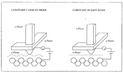
Atomic scale investigation of clean and epi-grown Si(001) surfaces using scanning tunneling microscopy
Tam metin
Şekil

Benzer Belgeler
Although it is possible to come across individual examples of minar- ets without mosques in different parts of Ankara, a striking setting of single minarets allowing for
The underlying motive for consideration of quantum EM radiation in terms of spherical waves of photons is the fact that the atomic and molecular tran- sitions create the
By contrast, as a woman, Barbara Greene is much less implicated in the imperialist tradition of travel writing, and at times Too Late to Turn Back disrupts some of the assumptions
The following theorem gives the covariance between the weights of a code with random generator matrix.... When we transform this theorem to the case of the random code C ⊥ the result
coursebooks. I am also exploring the attitudes of students towards the use of MALL applications as supplementary materials. Then, during the experiment, the participants in
When we compare these three impulse responses in column four, we observe that (a) a shock to interest rate is less persistent, (b) the effect on exchange is higher, (c) the decrease
Although T-cell A2BR plays an insigni ficant role for A2BR-mediated immu- nosuppression and tumor promotion, A2BR de ficiency in tumor- bearing mice caused increased in filtration
11 (b), the change of the laser power P, used to the processing of the Ti layer at a certain constant scanning speed υ in the NLL method, has a strong impact on the value of the
