Electrically controlled resistive switching assisted active ultra-broadband optical
tunability in the infrared
Enes Battal1,2, Ayşe Özcan2, and Ali Kemal Okyay1,2
1 Bilkent University, Department of Electrical and Electronics Engineering, Bilkent, TR-06800, Ankara, Turkey 2 UNAM - Institute of Materials Science and Nanotechnology, Bilkent University, TR-06800, Ankara, Turkey
*Tel:+90 (312) 290 1557, e-mail: [email protected]
Abstract- We present an electrically tunable optical device
with ultra-broadband tunability operating in 2-10 µm spectrum. We also, for the first time, optically observe resistive switching behavior in reflection measurements under electrical bias.
I.
I
NTRODUCTIONActive control of the optical properties of materials have always been of significance due to its various applications such as tunable optical filters [1], beam steering [2], adaptive sensors [3] and holographic devices [4]. Recently, nonlinear [5], electro-optic [6], magneto-optic [7], phase change [8] materials, doped semiconductors[9], liquid crystals [10], micromechanical structures [11] have been realized in order to gain control over the refractive index of an optical media. Yet, achieving optical tunability in a broad spectrum remains a challenge.
In this study, we experimentally demonstrate an electrically tunable optical device exhibiting ultra-broadband tunability characteristic in the mid-infrared spectrum. The proposed device consists of a p-n junction formed by ZnO/p-Si and an inherent memristor realized by addition of a metallic top contact (Al/ZnO/p-Si). We obtained a change of about 7% in the reflection spectra under electrical bias and also, for the first time, observed a hysteresis in the reflection spectra due to resistive switching.
II.
F
ABRICATION & MEASUREMENTSOn top of a highly p-type Silicon substrate, we deposited a blanket of ZnO thin film with 300 cycles of 200oC atomic layer deposition (ALD) using Cambridge Nanotech Savannah Thermal ALD. Then, the ZnO layer is isolated into an area of
600 µm x 300 µm using optical lithography and wet etching with H2SO4:H2O (2:100) solution. The deposited ZnO layer is previously shown to be highly doped with electron concentrations on the order of 1019 cm-3[12]. An Aluminum contact pad with fingers has been formed with consecutive optical lithography, thermal evaporation and lift-off processes. The final form of the fabricated structure is shown in Fig. 1. Electrical measurements are performed using top Al and bottom Si layers as contacts with Keithley 2400 Source Measure Unit. Optical measurements from the area with metallic fingers are performed using a Bruker Vertex 70 Fourier Transform Infrared (FTIR) spectrometer with a Hyperion 2000 microscope.
III.
R
ESULTS AND DISCUSSIONA voltage sweep loop between -6V and 6V is applied to the device with 1V steps. At each voltage step, reflection spectra of the device are measured in the spectral range of 2-10 µm, concurrently. This measurement loop is carried out twice for consistency. In Figure 2, reflection spectra at the wavelength of 2um as a function of bias voltage is depicted for both of the measurement loops. A maximum change of about 7% in the reflection observed. Considering the highly doped nature of both Si and ZnO layers, the optical characteristics of these layers in the spectrum of interest is dependent on the amount of free carriers according to Drude oscillator model in this spectrum. The depletion width increases under reverse bias and reduction in the number of free carriers in both ZnO and Si and induces a change in the reflection spectrum. Under forward bias, similar mechanism occurs but with an increasing concentration of free carriers in both layers with shallower
Figure 1 – Fabricated device structrure along with the voltage bias configuration
Figure 2 – A repeatable optical hysteresis in the reflection spectrum is observed when the bias voltage is swept in a loops.
570
WH3.5 (Contributed)
2:45 PM – 2:00 PM
depletion region. Therefore, any change in the number of free carriers would contribute to the change in refractive index of the dielectric layers, and alter the reflection spectrum.
We also observed a repeating hysteresis in the reflection spectra of the device. In order to evaluate such a hysteretic behavior, we measured the current-voltage (I-V) relationship with a voltage sweep. A repeatable memristive hysteresis is observed in the I-V relationship in Fig. 3. For both optical and electrical hysteresis, a contrast ratio of about 4 is observed. Due to very high doping of ZnO layer, the contrast ratio is observed to be very low. Such an optical hysteresis of a memristive device is observed for the first time in the literature.
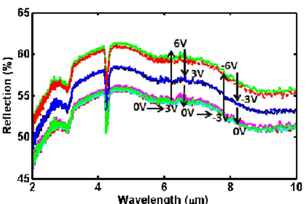
We also investigated the broadband characteristics of the electrical tunability of the reflection spectra along with its resistive switching behavior. For the wavelength range of 2-10µm and bias voltages between -6V and 6V with 3V steps starting from 0V, the reflection spectra is depicted in Figure 4. When the bias voltage is increased from 0V up to 6V or decreased down to -6V, the entire reflection spectrum increases by about 5.5%. Such tunability in a broadband spectral range is obtained with bias voltages that fall into CMOS compatible region. The optical hysteresis behavior observed in Figure 2 can also be seen in this figure such that the reflection spectrum is dependent on its past of the electrical bias. The reflection spectrum at 3V (or -3V) does not differ from that of 0V unless 3V (or -3V) is applied after returning from 6V (or -6V). We further investigated the mechanisms behind the optical observation of resistive switching and constant change in the overall reflection spectra.
IV. CONCLUSION
We demonstrated a broadband electrically tunable optical reflection device operating in the spectral range of 2 – 10 µm. We observed change in the reflection spectra as high as 6%. The bias voltages that are necessary for tuning are on the order of several volts. We also optically observed the memristive hysteresis of metal-oxide based structure. This study paves the way for the utilization of resistive switching behavior along with broadband tunability in optoelectronic device applications.
ACKNOWLEDGEMENTS
This work was supported in part by European Union Framework Program 7 Marie Curie IRG Grant 239444, COST NanoTP, TUBITAK Grants 109E044, 112M004 and 112E052. The authors acknowledge support from TUBITAK-BIDEB.
REFERENCES
[1] K. Diest, J. A. Dionne, M. Spain, and H. A. Atwater, Nano Letters, vol. 9, pp. 2579-2583, 2009/07/08 2009.
[2] E. Battal and A. K. Okyay, Opt. Lett., vol. 38, pp. 983-985, 2013. [3] S. M. Menke, R. Pandey, and R. J. Holmes, Applied Physics Letters, vol. 101, pp. 223301-4, 2012.
[4] N. S. Holliman, N. A. Dodgson, G. E. Favalora, and L. Pockett, Broadcasting, IEEE Transactions on, vol. 57, pp. 362-371, 2011. [5] A. E. Attard, Appl. Opt., vol. 38, pp. 3239-3248, 1999. [6] J. F. Lotspeich, Spectrum, IEEE, vol. 5, pp. 45-52, 1968. [7] A. Garzarella and W. Dong Ho, Ultra-Wideband (ICUWB), 2011 IEEE International Conference on, 2011, pp. 240-242.
[8] M. J. Dicken, K. Aydin, I. M. Pryce, L. A. Sweatlock, E. M. Boyd, S. Walavalkar, et al., Opt. Express, vol. 17, pp. 18330-18339, 2009. [9] C. Qiu, X. Ye, R. Soref, L. Yang, and Q. Xu, Opt. Lett., vol. 37, pp. 3942-3944, 2012.
[10] A. Minovich, D. N. Neshev, D. A. Powell, I. V. Shadrivov, and Y. S. Kivshar, Applied Physics Letters, vol. 96, pp. 193103-3, 2010. [11] L. Taelim, A. Higo, H. Fujita, Y. Nakano, and H. Toshiyoshi, Optical MEMS and Nanophotonics (OPT MEMS), 2010 International Conference on, 2010, pp. 107-108.
[12] E. Przeździecka, W. Ł, W. Paszkowicz, E. Łusakowska, T. Krajewski, G. Łuka, et al., Semiconductor Science and Technology, vol. 24, p. 105014, 2009.
Figure 3 – A resistive switching behavior is clearly observed in the current-voltage measurements.
Figure 4 – Spectral response of the device under electrical bias. Time history of the bias voltage is shown with arrows starting from left to right. The upward and downward arrows indicate the change In the reflection spectra.