by Ahmet Tuna
Submitted to the Institute of Graduate Studies in Science and Engineering in partial fulfillment of
the requirements for the degree of Master of Science
in
Electrical and Electronics Engineering
Bilgi University 2017
A PRESSURE SENSOR FABRICATED WITH 3D PRINTER FOR A BIOMEDICAL MICROSYSTEM
APPROVED BY:
Asst. Prof. Yiğit Dağhan GÖKDEL ………...
(Supervisor)
Asst. Prof. Baykal SARIOĞLU ………
(Co-Supervisor)
Asst. Prof. Okan Zafer BATUR ………...
Asst. Prof. Mehmet AYYILDIZ ………...
Asst. Prof. Revna ACAR VURAL ………...
ACKNOWLEDGEMENTS
It is an honor to thank those people who have helped me. Moreover, completion of the work would be impossible without them.
Firstly, I would like to thank my supervisors, Prof. Yiğit Dağhan Gökdel and Prof. Baykal Sarıoğlu for teaching me the subject, their suggestions, encouragements and showing great patience against me.
Beside my supervisors, I would like to the rest of my thesis committee, Prof. Okan Zafer Batur, Prof. Revna Acar Vural and Prof. Mehmet Ayyıldız for reading my thesis and sharing their invaluable ideas.
I would also like to give my special thanks to my friend Oğuz Kaan Erden for taking the tasks seriously in our research team and for his sincere helps.
It was a great happiness to work with my dear friends Ahmet Uğur Dilek and Hilal Kızılcabel in same laboratory. It was a wonderful experience to be in the same place with them. I am also grateful to my precious family, my dear mother Melek Tuna and my dear father Musa Tuna. Although we have been living in different cities, they have always had helped, favored, cared and loved me.
Additionally, I wish to thank my sincere friends Erbil Arık, Ayça Dilruba and Hacı Ali Kuşçu for their close friendships throughout my whole university life.
Subsequently, I would aspire to thank my dear friend Mert Aktürk for his encouragements, his friendship and help during tough times.
Moreover, I would like to express my gratitude to my kind-hearted friend Selçuk Keser for his careful helps.
Finally, I would like to thank TÜBİTAK for supporting this work under the project number of EEEAG 114E549.
ABSTRACT
A PRESSURE SENSOR FABRICATED WITH 3D PRINTER FOR A
BIOMEDICAL MICROSYSTEM
In this work, a novel 3D printed capacitive pressure sensor with a corrugated surface is presented. The design composed of top and bottom plates. The sensor is 3D printed using a commercially available polymer material and then coated with chromium and gold with sputtering process. The dimensions of produced structure that designed are 11 𝑥 11 𝑥 4.6mm3. Due to the corrugated surface, the area of the plates is increased 19.46% compared to a standard flat surface parallel plate capacitive sensor in the same bulk area. The design process of the sensor, simulation and the experimental results are given and explained in detail. The performance of the sensor is tested with various pressure levels between 0 Pa and 8.88 kPa. The experimental results show that the capacitance range of the sensor is 2.7 pF-4.3 pF. The maximum sensitivity of the sensor is obtained as 0.14 pF / kPa. The results confirm that the presented capacitive sensor can be utilized for carrying out pressure measurements.
Keywords: 3D printing, additive manufacturing, capacitive pressure sensor, corrugated
ÖZET
BİYOMEDİKAL BİR MİKROSİSTEM İÇİN 3 BOYUTLU YAZICI İLE
ÜRETİLMİŞ BASINÇ SENSÖRÜ
Bu çalışma, 3 Boyutlu Yazıcı ile polimer malzeme kullanılarak üretilen, dalgalı yapıda bir yüzeye sahip, kapasitif basınç sensörü ile ilgilidir. İlk olarak sensörün tasarımı yapılmış, tasarımın üretimi 3 Boyutlu yazıcı ile gerçekleştirilmiş, üretim çıktısı tozutma tekniğiyle, 10 nanometre kalınlığında krom ve 115 nanometre kalınlığında altın metalleri ile kaplanmış, kaplanan yapının bağlantıları bakır kablolar ve gümüş epoksi ile sağlanmış ve gerekli ölçümler yapılmıştır. Test sonuçları ise daha önceden gerçekleştirilmiş olan benzetim sonuçları ile karşılaştırılmıştır. Tasarım aşamalarında üretilen tüm yapı 11 𝑥 11 𝑥 4.65 (uzunluk 𝑥 genişlik 𝑥 yükseklik) (mm3) boyutlarına sahiptir.
Anahtar Sözcükler: 3 Boyutlu yazıcı, kapasitif basınç sensörü, dalgalı yüzey, eklemeli
TABLE OF CONTENTS
ACKNOWLEDGEMENTS ... iii
ÖZET ... v
TABLE OF CONTENTS ... vi
LIST OF FIGURES ... vii
LIST OF TABLES ... ix
LIST OF SYMBOLS & ABBREVIATIONS ... x
1. INTRODUCTION ... 1
1.1. PROBLEM STATEMENT ... 3
2. OVERVIEW OF CAPACITIVE SENSORS ... 4
2.1. TYPES OF THE CAPACITIVE PRESSURE SENSORS ... 4
2.2. APPLICATIONS OF CAPACITIVE SENSORS ... 6
2.3. SPECIFICATIONS OF CAPACITIVE SENSORS ... 7
2.4. CAPACITIVE SENSORS WHICH ARE MADE OF POLYMER MATERIALS ... 10
3. THEORETICAL DESIGN OF THE 3D PRINTED CAPACITIVE PRESSURE SENSOR ... 20
4. SIMULATION OF THE 3D PRINTED CAPACITIVE PRESSURE SENSOR ... 26
5. FABRICATION OF THE 3D PRINTED CAPACITIVE PRESSURE SENSOR ... 31
5.1. 3D PRINTING ... 31 5.2. SPUTTERING ... 35 5.3. IMPLEMENTED DEVICES ... 36 6. EXPERIMENTAL RESULTS... 39 7. CONCLUSION ... 46 REFERENCES ... 47
LIST OF FIGURES
Figure 1.1. Basic illustration of a capacitive sensor components. ... 1
Figure 2.1. Basic illustration a parallel plate capacitive sensor [6]. ... 4
Figure 2.2. Basic illustration of parallel comb capacitive sensor [6]. ... 5
Figure 2.3. One of the primary illustrations of single plate capacitive sensor for the distance tracking [6]. ... 5
Figure 2.4. Parylene-C polymer-based capacitive sensor [12]. ... 12
Figure 2.5. PDMS polymer based shear and normal force sensor [13]. ... 15
Figure 2.6. Change in capacitances which caused by (a) tegafur, (b) uridine, (c) flurouracil, (d) uracil, (e) m-aminophenol, (f) ascorbic acid and (g) mercapto ethylamine [14]. ... 16
Figure 2.7. The designed electronic structure is fixed to the polyphenyl sulfone (PPSF) that ... 17
Figure 3.1. Shows, design parameters in mechanical measurements for all design which will be explained. ... 22
Figure 4.1. Assigning the material properties. Vero Clear material properties and boundary load selection for left and right, respectively. ... 26
Figure 4.2. Assigning the mesh parameters. ... 27
Figure 4.3. The meshed result of the proposed design. ... 28
Figure 4.4. The total displacement of the top plate of recommended design under 2.8 kPa differential pressure. The central deflection of the plate is 3.77 micrometer at the vertical axis. ... 29
Figure 4.5. The horizontal effects of the applied pressure. ... 30
Figure 5.1. CAD image of the proposed top and bottom plate surfaces. ... 31
Figure 5.2. The basic illustration of a FDM manufacturing [50]. ... 33
Figure 5.3. Print-out of the mentioned AM technique ... 34
Figure 5.4. Implemented 3D printed capacitive sensor a) fabricated bottom plate, b) fabricated top plate, c) assembly of the fabricated bottom and top plates, d) profile view of the assembled sensor. ... 37
Figure 6.1. Experimental results of the applied pressures and capacitance results of the fabricated sensor under pressures between 0 Pa and 8.88 kPa. ... 39 Figure 6.2. Curve fitting between experimental result and characteristic equation of the
proposed sensor. ... 40 Figure 6.3. Experimental results of the obtained capacitances and sensitivity of the fabricated sensor under pressures between 0 Pa and 8.88 kPa. ... 41 Figure 6.4. Experimental setup and read-out circuitry of the design ... 44
LIST OF TABLES
Table 3.1. Dimensions of the proposed design ... 25 Table 5.1. Material properties of the Vero-Clear RGD 810 [34]. ... 32 Table 6.1. Obtained results of sensor specifications ... 42 Table 6.2. Comparison between different works based on sensor specifications. BM is Bulk Micromachining, SM is Surface Micromachining, PB is Polymer Based and SB is Silicon Based. ... 43 Table 6.3. Comparison between different works based on sensor specifications. BM is Bulk Micromachining, SM is Surface Micromachining, PB is Polymer Based and SB is Silicon Based. ... 43 Table 6.4. Resistance values of the parasitics between RLC meter and sensor. Resistance values R1-R6 are pointed in Figure 6.4. ... 45
LIST OF SYMBOLS & ABBREVIATIONS
C Capacitance
C0 Initial capacitance
ΔC Capacitance change
ε0 The electric constant
εr Relative dielectric constant
A Area d Distance w Width L Length S Sensitivity V Voltage Q Charge
𝐷
⃗⃗
Electric displacement field between upper and lower plates𝐸⃗
Electric fieldB Amplitude of wave
λ Wavelength
x1, 2 Side length of the raised structure for epoxy w1,2,3,4 Side lengths of plate rectangle
r1 Diameter of legs
r2 Diameter of holes
h1 Leg length
h2 Hole depth
t1 Thickness of the membrane t2 Thickness of the bottom plate
𝜎0 Membrane stress
p Pressure
a Width of the moving part of membrane
ω0 Vertical displacement
E Modulus of elasticity ρ Electrical resistivity Acs Cross-sectional area
AM Additive Manufacturing
3D Three Dimensional
CAD Computer Aided Design
PDMS Polydimethylsiloxane
MEMS Micro-Electro-Mechanic-Systems
LIGA Lithographie Galvanoformung Abformung
FDM Fused Deposition Modeling
SLA Stereolithography
SLS Selective Laser Sintering
LOM Laminated Object Manufacturing DLP Digital Light Processing
SLM Selective Laser Melting
EBM Electronic Beam Melting
PCB Printed Circuit Board
PPSF Polyphenyl Sulfone
PET Polyethylene Terephthalate
SI International System
FEM Fused Deposition Modeling
FFF Fused Filament Fabrication
PVD Physical Vapor Deposition
1. INTRODUCTION
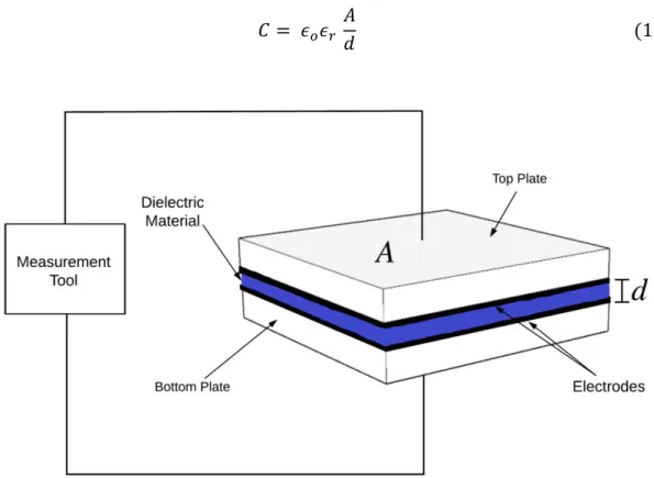
In general, capacitive sensors are formed by two plates, two electrodes, dielectric material, connecting materials and the device that used for measurement. The change in the distance between the electrodes with an external effect results in capacitance change. The capacitance is measured, and as a result, a relation can be set between the first mechanical input and the last-obtained change in capacitance. The described working principle is precisely shaped according to the following equation [1-2].
𝐶 = 𝜖𝑜𝜖𝑟 𝐴
𝑑 (1.1)
Figure 1.1. Basic illustration of a capacitive sensor components.
Where C is the capacitance value, εr is the relative dielectric constant of the dielectric material between the plates, εo is the permittivity of free space, A is the surface area of the plates and d is the distance between the plates. Capacitive sensors can be designed in different ways depending on the application. Some of these can be classified as parallel plate, parallel comb and also single plate [6]. Capacitive sensors have more advantages over the alternatives. It has more advantages especially in sensitivity to adopt it high-input applications.
Also, it can be developed to be manufactured at low impedance and to suppress parasitic effects. Furthermore, it allows changing the prototype to improve the operation process for all system [3-5]. These advantages and more are included by capacitor sensors in recent advances.
Capacitive sensors can be manufactured by using different materials. Type of materials vary according to where the sensor will be utilized and which fabrication processes are to be chosen to produce. Moreover, it increases the variety of the material to improve different kind of fabrication techniques. Those are fabrication capabilities, can be observed in manufacturing process of capacitive sensors. For example; deposition methods, measurement techniques, protection and bonding opportunities such as sputtering, 4-point-probe technique, permalloy applications and gold bonding processes, respectively.
The primary purposes of the sensor plates are holding the electrodes and providing movement capabilities to the sensor such as moving to downward and upward or throughout horizontal axis. Furthermore, plates are used usually for controlling the area that can be observed in Equation (1.1) to gain more capacitance. The plates of a capacitive sensor can be formed by using materials such as polysilicon, silicon oxide, silicon nitrite [2]. However, for additive manufacturing (AM) technique thermoplastic polymers could be used additionally.
For a capacitive sensor, another basic element is called electrode. Electrode means a conductive material that is usually located very near to plates and it has capacitance value by containing charge through the surface area. Preferred conductive materials are generally metals such as gold, copper, chromium, silver, nickel or iron. For these metals, they are chosen generally because they have high conductivity values. Such kind of metals help the system to work with lower parasitic resistances and higher conductivity values.
Between the electrodes, the other used component is dielectric materials. Dielectric materials are used as a layer and that is usually made of insulating materials. The one of the main reasons of why mostly preferred layers are insulators is using it to change the “εr“parameter. Secondly, it is preferred to protect the electrodes contact each other. This protection is to do not let them touch even in pull-in state for providing touch mode active responses [47]. Those can be rubber, polymer, wood or even air. Therefore, dielectric materials can be used for not only increase the “εr“ parameter but also for protection of touching the electrodes.
When a capacitive sensor is operated, the amount of distance between the top plate and bottom plate changes.
The mechanical input such as pressure need to be converted into an electrical signal such as capacitance. Finally the electrical signal must be monitored and this visualizing tools can be named as monitoring units. For instance, some devices can be a voltmeter, capacimeter, amperemeter, multimeter, ohmmeter or a RLC meter.
Bonding units can be explained as an important component of a capacitive sensors. It is a connection between the system and monitoring units that it always desired to be ideal as possible. Cables, connection points, connectors and other units such as glue and epoxy should be designed and installed well. Moreover, parasitic relations between bonding units and rest of the system need to be controlled according to the desired resistivity and conductivity responds. Copper cables and silver epoxy can be given as an example of bonding components.
In general perspective, capacitive sensors can be explained as above. At this point of view, capacitive sensors in the literature can be seen in wide variety of applications. All in all, published works have shown an incremental graph from 1945 to 2017 for capacitive sensors. In these works, capacitive sensors can be seen in different forms [6-7].
Although, there are different kind of capacitive sensor designs, it is fact that, for recent advances, it cannot be used full efficient and the capability of designs cannot be fully enough to provide sufficient outcomes for all technological developments.
1.1. PROBLEM STATEMENT
Basically the performance of various micro-electro-mechanical-systems (MEMS) applications depends upon devices and microstructures with an alternating thickness. Standard micromachining technologies including surface micromachining [17], bulk micromachining [18] and LIGA [19] are not able to form curved three-dimensional (3D) surfaces and therefore cannot always pattern the required profiles of micro-structures. Even though several different reported methods are claiming to pattern out-of-plane curved surfaces on polymer and silicon substrates namely micro stereo lithography [20] or inclined/rotated UV lithography [21], they are not entirely capable of producing real 3D microstructures with a low-cost and in quick fashion. As a result, the explained all of absences can affect dramatically recent advances especially for capacitive sensors manufacturing.
2. OVERVIEW OF CAPACITIVE SENSORS
In this section, those are explained that basic components, general forms, application areas and explanation of specifications are given for capacitive sensors. Lastly, a review of capacitive sensors is also provided.
2.1. TYPES OF THE CAPACITIVE PRESSURE SENSORS
First of all, the parallel plate capacitive sensors are mostly used type. The application variety in advances has been expanded by parallel plate capacitive sensors. Similarly, the main working principle of this type capacitive sensor is to create a voltage difference between the parallel two electrodes by applying any loads to the plates. An example is illustrated in Figure 2.1. The voltage difference is to be controlled by changing the parameters "w", "L" and "d" and these parameters are shown in Figure 2.1.
Figure 2.1. Basic illustration a parallel plate capacitive sensor [6].
Then secondly, the other class to be explained as capacitive sensor is parallel-comb type that is designed as interdigitated structures to have higher sensitivity in the same restricted area or even in a smaller region. Particularly, due to the usual methods such as planar silicon process, polymer-based material technologies, surface micromachining and bulk micromachining the capability of productions such for capacitive sensors have been frequently improved for the requirements of applications. Main structure of this type is shown in Figure 2.2.
Figure 2.2. Basic illustration of parallel comb capacitive sensor [6].
The other type is single plate capacitive sensors that is another example to be usual in advances. Working principle is based on using an object to be detected as a secondary electrode. Generally, this type of sensors is used in distance measurement. Also, this method can be considered for fingerprinting or character identification processes. The general structure is shown in Figure 2.3. that shows a distance sensing method by using a single plate capacitive sensor. Also, it can be used where the approaching object is able to be seen to be as another electrode. Thus, the distances between the objects can be detected if and only if the related parameters besides the distance are known at first.
2.2. APPLICATIONS OF CAPACITIVE SENSORS
Capacitive sensors can be used in many areas. These areas will be discussed in the next paragraphs. Generally, the measurement capabilities of the sensors based on the kinds of inputs are needed to be detected. For example; pressure, humidity, acceleration can be given as the inputs. Moreover, it is also important to determine which magnitude is changed in the process because of these inputs [6-8].
First of all, one of the most common measurement type of capacitive sensors is pressure measurements. The solid, liquid and gas pressures can be measured with the sensors which are capable to measure pressures. If area and/or distance of the capacitors are changed by any solid, liquid or gaseous input, this changes total capacitance so it can be measured by providing a relation between total capacitance and the inputs.
Secondly, amount of humidity can be detected and measured by using its moisture rate. In humidity measurements, moist air is used as a dielectric material. The dielectric coefficient of air is 1. By knowing rest of the parameters of reference capacitive sensor, it is possible to calculate the moisture rate that is hold by the air. In other words, if the results are not same with 1 that means the air contains moisture.
Moreover, capacitive sensors are widely used for measuring acceleration. Acceleration measurements require the placement of a mass-weighting device in the sensor. The moment of inertia created by the weight moves between plates and thus determine how much acceleration is obtained by the capacitance change that would occur between the electrodes.
Also, a distance can be calculated with a capacitive sensor by locating the sensor plates at beginning and end points of the distance which is desired to be measured. That gap measurement can be quite sensitive according to quality of the capacitive sensor. For gap measurements, it is usable for knowing all parameters of the system except the distance between the electrodes.
Also, it is possible to reveal the sensor properties with using another sensor. This can be named as sensor detection measurement. On the other hand, a material identity and dimensions of material can be detected by using such a reference capacitive sensor. It shows us if any dielectric material is located between the electrodes of the sensors, the thickness of the material can be detected by knowing the dielectric constant or by knowing the thickness of the material it can be identified what the material is.
Besides of these, it is also possible to detect the form of a matter. For example, the amount of ice can be measured for a research contains icy environment. In the method of measuring the ice amount, the changing in capacitance and the electric field of electrodes which located in an icy environment shows us how much ice exist by correlating them numerically. This method is widely used in airplanes, mines or aerospace engineering.
Moreover, for positioning the structures in a building and structural engineering works, capacitive sensor can be used for angle measurements. In this method, the necessary process is adding a third angular orientation to the movement of the electrodes. The capacitance change which is caused by an angular variation of another insulator is to be measured.
Also the other most common method to say about where the capacitive sensor can be used is key opening-closing systems. In electrical systems, capacitive sensors are utilized in the on-off switches. A capacitance change can be directed to the system, so the on-off operation can be performed.
2.3. SPECIFICATIONS OF CAPACITIVE SENSORS
For all capacitive sensors, there are lots of characteristics to understand the sensor qualifications. Commonly, most of them are that reveal sensor quality. The general specifications are presented below[9].
The key specification of a sensor is sensitivity. The sensitivity is a quality that shows how much the sensor is capable to respond such a small amount of input.
That is to say, it is usually expressed as,
𝑆 = 𝑀𝑒𝑎𝑠𝑢𝑟𝑒𝑚𝑒𝑛𝑡
𝐼𝑛𝑝𝑢𝑡 𝑆𝑡𝑖𝑚𝑢𝑙𝑢𝑠 (2.1)
where S is the sensitivity. For example, when we compare a couple of capacitive pressure sensor that first one can convert 50 Pa to 30 pF and second sensor takes the input as 10 Pa and converts to 100 pF, this is obvious that the second sensor is extremely more sensitive than first one.
Another specification of a sensor is range. The range is the appropriate area for a sensor that senses and responds well in this region. It has been called as bandwidth or effective bandwidth. It is important to obtain the range characteristic of a sensor to adopt it into the desired system. For example, if a depth pressure sensor which has 5m to 100m measurement and if it will be used into 300 m depth, this condition may damage the sensor or it may give some erratic outputs.
The accuracy is one of the basics that shows whether the sensor responds are clear or not. It also defines specifically; how close the sensor is to the correct responses. For example, a capacitive pressure sensor senses the finger-prints as 8.921, 10.002 and 12.117 kPa, while the actual result must be 10 kPa, it means that the sensor has good accuracy but bad precision (defined in following paragraph).
Besides of the accuracy, the precision is one of the other definition of rate of clear results. This shows quality of sensor gives us the responses if they are coherent with each other. For example, a capacitive pressure sensor senses the fingerprints as 5.05, 5.03, 5.04, and 5.03 kPa while the actual result is 10kPa, it means that the sensor has good precision but bad
accuracy.
The repeatability is another qualification as a sensor specification that it can be explained as the repeatability between all possible outputs regardless the outputs is correct or not. Therefore, in some case, a sensor can be repeatable with no accuracy and no precision qualifications.
The drift is one of the most undesired effects of a sensor. It is a small frequency change in time.
The disadvantages of drift are, first it is one of the major element to get a sensor old and it may affects negatively the mentioned sensor abilities by itself.
However, if the drift occurs smoothly and it can be observed in a stable case, it can be corrected by using some error correction method but it is a rare situation to take it as a solution.
The hysteresis is a general problem (mostly for pressure sensors) that causes uncertain mechanical motion, i.e., making the membrane movements unpredictable, due to the internal stresses. Thereby the stress blocks the next inputs and blocks the sensor to behave in a stable system characteristic. For example, in a capacitive pressure sensor there must be internal stresses created by an input. Then those stresses affect the next deflection of the sensor in the next operation by creating a negative or positive feedback through the membrane. Moreover, the stability is another approach for the drift, accuracy, and precision. It is not only a name of ability for a sensor to be resulted with the same output or not, but an internal approach to repeatability. This property can be called as another aspect of the accuracy but mostly, as an overall aspect of precision and drift.
The response time of a sensor defines the duration of output that is created by an input so it
is a time definition between input and output into the process.
The self-heating means that, in some sensors, we need to apply current through the resistor to measure some quantities. Similarly, in that case, the heating will occur. This condition comes with some additional requirements. Heating is one of the most dangerous cross-talks to damage the sensor, and it must be controlled in an optimized way.
Settling time is an amount of time that is required for sensor to reach a stable output after
applied energy at beginning of an operation. In other words, it is a turning-on time that the ability is especially important for the multi-process sensors that require more than one on-off process due to the requirement of several settling cycle.
Then the voltage requirement is one of the definitions of power consumption ability that it is crucial for safety of the device. In other words, it is a range to work sensor well in most of the operations. In the case of exceeding the interval may cause burning out of the sensor. Then, being below of this range may affect to have insufficient energy to operate the system. The internal parasitic effects of whole devices are to influence this specification highly.
Current drawn is another definition for being one of the power qualifications of a sensor.
The amount of drawn current is basically related to the voltage requirement and voltage usage. (Simply, the sensor draws almost constant power which is current times voltage.) As a result, to control power specifications of the sensor, current and voltage should be known as parameters.
The output specification is another range about voltage output of the system. For instance, a capacitive pressure sensor transmits the information as a voltage in the range of between 0 and 5 V. In the processes, it is to use modulated waves (sine, square, triangular waves) or other information transmitting options in signal processing. Therefore, in the systems of capacitive pressure sensors, information is not transmitted as a capacitance but the voltage transmission is used as the output specification.
The specification of the fit calibration to equations means that it is a qualification for well-calibrated response of the device with not only outputs of a standardized sensor but also to aim to fit with theoretical equations.
The sensor-noise estimation is a qualification and an error result that is another crucial parameter to be detected and to be corrected in a system. Not only some environmental noises but also inherent noise effects must be detected to obtain the signal characteristic correctly. One of the ideal methods in the process order of noise estimation is, first detecting noise environment and in addition to this, finding out the internal noises with using before environmental information. In other words, this method provides us a solution only if the sensors' noise does not affect signal level.
As those are explained above, a capacitive pressure sensor has many different qualifications and specifications. Basically, the specifications of the proposed sensor are given in the experiment section.
2.4. CAPACITIVE SENSORS WHICH ARE MADE OF POLYMER MATERIALS
In this part, some applications of capacitive sensors made of polymer materials are discussed. Additionally, some piezo-resistive sensors are mentioned as examples of the polymer-based manufacturing.
A considerable rate of the capacitive sensors is made of polymer materials. Polymer-based capacitive sensors have the well-known capacitive sensor operating principle.
There is no functional difference as operating principle, but making the system with polymer based materials.
The reason of using is the materials are many in the field; as well as being low-cost, quick prototyping and usable. It is possible to shape them in desired form easily. It has the capability of rapid shaping. Generally, polymer-based capacitive sensors are applied to the plates, so that the plate can be bent, folded, extended and shortened. Thus, since changing of the shapes of the plates can cause capacitance changes, this can be monitored and converted to an electrical signal as above explained principles which has similarities with that.
An example of basic polymer-based capacitive sensor that is known in the literature is published by G. Delapierre [10]in 1983. In this paper, a humidity sensor is reported based on a polymer-based design. Also, the characteristics of this work with polymer materials and experimental results can be observed.
Another publication is published in 1985 by Peter J. Schubert and Joseph H. Nevin [11]. In this work, a capacitive humidity sensor is introduced. Polyimide polymer material is used. Briefly, the working principle is based on change of the dielectric coefficient of the polyimide material by moisture.
The D. Briand's work in the literature is another example for polymer-based capacitive sensors [12]. In this study, electrodes in comb structure are coated with a perylene-C polymer material. The study is illustrated in Figure 2.4. Main purposes of the polymer material are to provide for being a good physical protection, to form a bendable structure and to use it as a contact shield.
Figure 2.4. Parylene-C polymer-based capacitive sensor [12].
There are many polymer options to use in different applications for designing and manufacturing polymer-based capacitive sensors. Several preparation techniques have been developed to adapt the conductive polymers to form it as an active layer of a sensor on different sensitive materials and for various types of sensors. Some of them are explained below as well as the techniques can be used for depositing conductive layers upon the active surface of the sensor.
Firstly, the electrochemical deposition can be given as an example of a fabrication technique for polymer on active layer. Additionally it can be used for monomers or metals. It is one of the most suitable method for preparing conductive films. The thickness of film can be controlled by the total charge passes through the electrochemical that is used during growth of the film. In fact, the deposition must be done on a conductive substrate. As long as the insulating gap (generally designed as a few tens of micrometers) between neighboring electrodes are close enough, the growing film can connect the electrodes. This is an important point to avoid in the manufacturing of semiconductor devices.
Secondly, when a substrate is immersed into the chemical polymerization, monomer or metal solution, deposition can be occurred on the surface. It is so called as immersion coating. The process also occurs on different substrates, and the film thickness is generally controlled by the duration of the dip. A similar process may alternatively be applied by immersing the substrate into the monomer or oxidant. The adsorbed monomer is able to polymerize at the surface of substrate.
Another way for deposition can be mentioned as spin-coating technique. It is a simple way to prepare films from soluble conductive polymers. In this process, the conductive polymer solution is sprayed onto a rotating substrate. After evaporation of the solvent, a thin film can be formed. This process can be repeated by checking the thickness of the film. The concentration of the solution and the rate of rotation of the substrate have major role in setting the thickness of the film. This method can be used to coat conductive polymers on both conductive and insulated surfaces.
Moreover, the LB technique can be chosen for growing layer. It can be applied for a thin film on surface active material so it is one of the convenient methods. With the LB technique, the film can be prepared directly from the polymer. By the polymerization on the monomer substrate, the LB film can be ultra-thin (single molecular layer) so generally it is to be obtained by repeating the process to have lesser thickness if it is necessary.
Moreover, in another technique, the process can be performed with a polymeric anion solution and a polymeric cation solution. The solutions provide the preparation of a different composite film of two polymeric electrolytes. Also, the method might be called as self-assembling layer technique. It allows to attach of a polymeric anion on a polymer with a positive charge in the main chain.
Furthermore, the other deposition opportunity is thermal evaporation. This technique is based on a principle that is a conductive material can be heated under vacuum and attached to the target substrate by evaporation. The thickness of the formed film layer can be controlled by the duration of the evaporation process.
The other method is vapor deposition polymerization. This technique consists of two steps, preparation of a film layer characterized by an oxidant which is an initiator, and attachment of the vapor phase monomer onto the film. This technique is not only about preparing a pure conductive polymer film, but the preparation of composite film layers by employing different conductive polymers that can be applied.
Another technique for depositing polymer onto substrate is drip coating. In this technique, a polymer solution is dripped onto the substrate, as well as a monomer and an oxidant (initiator) can be prepared by dropping the solutions onto the substrate separately. This technique is simpler than the others but usually the film layers are obtained as they are not homogeneous.
In conclusion, we have the opportunities to coat with different polymer materials by the coating methods given above examples. These polymer options are quite common. Besides of these options, the works where they are published give us more examples for further opportunities as fabrication techniques about polymer materials.
Subsequently, polydimethylsiloxane (PDMS) is one of the most widely used polymer type. It can be given that the work which is performed with this polymer by Ming in 2010 as a published paper [13]. In this study, normal and shear forces are measured and the capacitive sensor designed with PDMS. Figure 2.5 shows an illustration of this work.
Figure 2.5. PDMS polymer based shear and normal force sensor [13].
Another example of polymer types used for polymer-based capacitive sensors is m-aminofen which can be utilized by doing electro-polymerization method. An example for this polymer and method is the work that is published by Liao in 2004 [14]. In this study, m-aminophenol is plated onto a gold electrode. Comparison of concentrations between other materials and m-aminophenol which is used in the study with the graph of capacitance change are shown next in Figure 2.6.
Figure 2.6. Change in capacitances which caused by (a) tegafur, (b) uridine, (c) flurouracil, (d) uracil, (e) m-aminophenol, (f) ascorbic acid and (g) mercapto ethylamine [14].
Another recently used polymer material is BaTiO3 (poly barium titanium oxide). It is a composite material that an example for this is done by Vithyasaahar [15] published in 2008. In this work, capacitive and resistive sensors are coated with BaTiO3 powders composed of particles that are 2 µm in diameter. The main purpose of the study is to achieve a large dielectric coefficient. Also, it is to take control the yield of the materials during the processes.
Moreover, it may be possible that practical results obtained from resistive sensors are reflected in the theoretical studies in capacitive sensors to estimate the performance of these sensors. An example of the study is published by obtaining a blend of polymers. An example for these composite materials that are common in application areas is published in 2013 by Je Dobrzynska [16]. In this study, Polyamide, Parylene-C, and PDMS are mixed with each other as a combined dielectric material after a standard metallization process. The process is performed for the sensor designed with the polymers to respond forces that applied in three axes (x, y, z).
Furthermore, recently, there has been an enormous interest in 3D printing technology which is also referred as additive manufacturing (AM) especially in the development of various MEMS as it is elaborated in previous sections. The 3D printed capacitive sensors has been being used to measure pressure, acceleration and humidity. However, the capacitors cannot be manufactured unless using only non-metal cartridges because the plates are electronic circuit elements that store electric charge. However, structures made of polymer materials by 3D printers are designed in the literature generally to gain linear characteristic. Polymer materials provides that it can be used for a supporting material. Partly, the structures produced for direct using as capacitive sensors, cannot be used as they are removed from the printer but must be exposed to some metal coating processes. An example of the method mentioned above is the designs confirmed in 2013 by Shemelya C. [22]. The main purpose of the polymer material used in this design is creating a support for the structure. The polymer type that is used in this work is polyphenyl sulfone (PPSF), and the result of this work is illustrated in Figure 2.7.
Figure 2.7. The designed electronic structure is fixed to the polyphenyl sulfone (PPSF) that printed-out from a 3D printer [22].
As mentioned in the previous paragraphs, it is possible to print metals by 3D printer, which means that printing electrodes directly for capacitive sensor designs is another opportunity. As an example of this type of works we can give the article that is published in 2012 by B. B. Narakathu [28]. In this work, all the materials produced by a 3D printer. The electrodes that are produced by a 3D printer are silver and the used polymers are polyethylene terephthalate (PET) and polydimethylsiloxane (PDMS). However, recently, while in some ways it may seem reasonable to print metals with 3D printers, it is slower, expensive and difficult to shape as a method compared with the applications of polymer materials.
Especially in thickness control, the metal layers cannot be printed below micrometer scales whether it is done by recent technology or not.
Many more examples can be found in the works in literature according to the needs. All of them can provide some advantages in different positions. After comparing the advantages and disadvantages of these studies, it is predictable to be needed to combine the advantages of these mentioned different structures. The comparison tables between some works in the literature are elaborated in Table 6.2 and Table 6.3 in the section of Experimental Results. Furthermore, especially in recent advances, there has been an enormous interest in 3D printing technology which is also referred as additive manufacturing (AM) especially in the development of various micro-electro-mechanical-systems (MEMS) because of its excellent fine feature detail, low-cost, low-waste and quick-prototyping capabilities [22-25]. AM techniques such as fused deposition method (FDM), stereolithography (SLA) or Selective Laser Sintering (SLS) employs deposition of materials layer-by-layer as oppose to conventional fabrication processes. Moreover, different from the planar microfabrication processes, AM fully enables the depth profile shaping of MEMS structures.
Different capacitors and capacitive sensor structures that are fabricated using 3D printing technology were previously shown in the literature [22, 26-27].
In order to increase the production speed and reduce the cost, 3D printers are utilized. They are adopted to production of sensors with help of the developed technologies. 3D printers are to be used with various of production methods to manufacture the sensors by different fabrication techniques. Thus, 3D printed sensors have been emerged as a new production technique. In 3D printers, various polymer materials such as nylon, acrylic, carbon fiber and even metals can be used as cartridges. Among these materials, metals are mostly used in electronic circuit designs, PCB productions and robotics for parts or design production. At the same processes, other polymer-based materials are used commonly in parts production. In addition to that, some special structured polymer materials and metals can be also used to make sensors. Such as inductive, resistive and capacitive sensors that are designed to measure heat, humidity, acceleration and pressure.
In the proposed work, it is focused on the design and fabrication of a novel capacitive pressure sensor that approaches the AM for designing the plates of the sensor and hence enhances the performance of the MEMS device.
It is organized as follows that, the next section explains the proposed capacitive pressure sensor design, design perspectives and elaborate its working principles. Moreover, working principles show how a parallel-plate capacitive sensor with a corrugated surface increases sensing performance. In section four, the FEM simulation process is discussed. Section five fully describes the implementation process along with an explaining of used fabrication material. Section six characterizes the devices by giving experimental results and discusses the performance of the proposed system. Then, concluding remarks and outlook are provided as it is required.
3. THEORETICAL DESIGN OF THE 3D PRINTED CAPACITIVE
PRESSURE SENSOR
The proposed 3D printed corrugated sensor design are shown in Figure 3.1 to elaborate the structure and the design parameters. The proposed design is composed of two parts; namely top and bottom plates. The top plate is designed to act as a membrane that can be deflected with an applied pressure. By coating the plates with a conductive material, parallel plate type capacitive pressure sensor structure is achieved. As it is depicted in Figure 3.1, the top plate contains legs interlocked with the holes located on the bottom plate to restrain only the vertical deflection of the top plate, by preventing the upper plate from lateral motion under an applied pressure. Theoretically, for the parallel plate capacitive sensors we apply voltage V to the plates to produce the total flux. In other words, the coulombs charges for the plates are produced by the potential difference (volts). It can be shown as below. Coulombs/volt expression can be written and named as capacitance C.
∆𝑉 = ∆𝑄
𝐶 (3.1)
When we located an infinite parallel plate into space with no free charges, the below situation can occur (but this is not a valid approachment for a capacitive sensor). There is an equality between charge density and amount of D field (D field is the electric displacement field between upper and lower plates) in SI (international system) units. Therefore, it goes to the Gauss’s law with integrating over an infinitesimally small rectangular box by first considering a one plate of a capacitor. [39, 52].
∮ 𝐷. 𝑑𝐴 = 𝑄𝑓𝑟𝑒𝑒 (3.2) 𝐴
Because of the infinitesimal dA is perpendicular to the field that is located upon box sides, it can be said to be the integrals for this section is zero.
However the space that is observed in the capacitive sensor (additional fields of the two upper and lower plates) can be expressed as below.
|𝐷| =𝑄𝑓𝑟𝑒𝑒
𝐴 (3.3)
Where A is surface area of the explained box, 𝑄𝑓𝑟𝑒𝑒
𝐴 is the charge density free on the positive plate. The fields of two plate can cancel each other around outside of the capacitive sensor so it can be said to be |𝐸| = |𝐷| = 0. Moreover, if we fill the gap between upper and lower plates with a homogeneous dielectric material with permittivity 𝜀 where (𝜀𝑟= 𝜀𝑟 × 𝜀0), the charge of 𝑄𝑓𝑟𝑒𝑒 would be kept similar as before. Whole electric field between the upper and lower plates must be smaller than explained D by a factor of 𝜀𝑟 as |𝐸| =
𝑄𝑓𝑟𝑒𝑒
𝜀𝐴 . Furthermore, if we kept constant the potential difference V and electric field E, subsequently, the stored charges increase. The increasing occurs by a factor of 𝜀𝑟.
Moreover, we can obtain the capacitance which is defined in a finite case, as below only if the linear gap between the plates is smaller than horizontal dimensions of the plates. In fact, it is an approximation from an infinite to a finite case in which, is only defined above approach but this model that is showed below as a frequently used equation for all capacitors. It can be also used for capacitive sensors or a system that possible to relate with above explanations. 𝐶 =𝑄𝑓𝑟𝑒𝑒 𝑉 ≈ 𝑄𝑓𝑟𝑒𝑒 |𝐸|𝑑 = 𝐴 𝑑𝜀 (3.4)
Finally, for the proposed design, the capacitance value of the proposed sensor geometry can be approximated by the equation below.
𝐶 = ∫ 𝐴
∫ 𝜖0𝜖𝑟𝑑𝑥𝑑𝑦
𝑑(𝑥, 𝑦) − Δ(𝑥, 𝑦) (3.5)
Where C is the capacitance value obtained under a differential pressure, 𝜀𝑟 is the relative dielectric constant of dielectric material that located between the top and bottom plates,
𝜀0 is the dielectric constant, d(x,y) is the distance between plates and ∆(x, y) is the function that models the deflection of the top plate [7]. When a mechanical force as a pressure is applied on the top plate, the top plate deflects and the distance between plates is reduced accordingly. The nominal distance which is a distance with zero-pressure is denoted with
d(x,y) in equation (3.5). For a standard parallel plate capacitor d(x,y) is a constant value.
Equation (3.5) clearly shows that the capacitance value of the proposed design is linearly depended on the surface area of the plates. It is important to note that the augmentation of surface area and therefore the capacitance increasing is advantageous since higher-valued capacitive sensors are desired for large full-scale range and for designing compact read-out circuits in any small restricted area. In order to attain a drastic augmentation of capacitance value, the surface area of the plates must be increased. Such a maximization in surface area can be acquired in a controlled manner by modeling the surface of the plates with a two-variable-function f(x,y). In the proposed design, to maximize the surface area in the same limited plate perimeter the following sinusoidal function is employed in both x and y-axes of the top and bottom plate surfaces,
𝑓(𝑥, 𝑦) = 𝐵 (sin (2𝜋
𝜆𝑥𝑥) + cos ( 2𝜋
𝜆𝑦 𝑦)) (3.6)
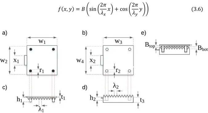
Figure 3.1. Shows, design parameters in mechanical measurements for all design which will be explained.
which results in corrugated top and bottom plate surfaces. In eq. (3.6), B is the wave amplitude then, λx and λy defines the wavelength for x and y dimensions, respectively [31].
Top and bottom plate surfaces that are modeled using equation (3.6) are illustrated in Figure 5.1.
The increasing in the amount of the proposed surface area can be approximated by considering a nominal distance d(x,y) and deflection ∆(x, y) functions between plates in equation (3.5). The distance between plates for the proposed capacitive sensor depends on the parameters of the applied surface function (3.7), thus, it varies along the x and y axes. The function for approach to the distance between plates can be expressed as,
𝑑(𝑥, 𝑦) = ℎ1− ℎ2− 𝑓𝑡𝑜𝑝(𝑥, 𝑦) + 𝑓𝑏𝑜𝑡(𝑥, 𝑦) (3.7)
where h1 and h2 are illustrated in Figure 3.1. ftop (x,y) and fbot (x,y) express the surface (function (3.9, 3.10)) for top and bottom plates, respectively.
Finally, expression of ftop (x,y) and fbot (x,y) in the main equation as d(x,y) are showed below.
𝐶 =∫ 𝐴
∫ 𝜖0𝜖𝑟𝑑𝑥𝑑𝑦
ℎ1− ℎ2− 𝑓𝑡𝑜𝑝(𝑥, 𝑦) + 𝑓𝑏𝑜𝑡(𝑥, 𝑦)− Δ(𝑥, 𝑦) (3.8)
To show final form of the approximation, in the denominator part of the function, ftop (x,y) and fbot (x,y) can be expressed more clear as can be seen below.
𝑓𝑡𝑜𝑝(𝑥, 𝑦) = 𝐵𝑡𝑜𝑝(sin ( 2𝜋 𝜆𝑥𝑡𝑜𝑝 𝑥𝑡𝑜𝑝) + cos ( 2𝜋 𝜆𝑦𝑡𝑜𝑝 𝑦𝑡𝑜𝑝)) (3.9) 𝑓𝑏𝑜𝑡(𝑥, 𝑦) = 𝐵𝑏𝑜𝑡(sin ( 2𝜋 𝜆𝑥𝑏𝑜𝑡 𝑥𝑏𝑜𝑡) + cos ( 2𝜋 𝜆𝑦𝑏𝑜𝑡 𝑦𝑏𝑜𝑡)) (3.10) Besides of that, the restriction of the range can be expressed by fracture stress of material used in the process. With the surface parameters of corrugated diaphragm, it can be also used for approach to the effective range of sensor. Furthermore, the latter effect can correspond the restriction of range such the plates cannot move when they are touched to each other.
On the other hand, for the relationship between the force exerted on the upper plate and the amount of deflection, the exerted force must be identified so that the required measurement will be able to be successfully expressed. In this review mechanical approaches of the material, especially stability aspects are important to take into equation as parameters which is desired to provide correct determination. As indicated in Table 3.1, the upper membrane thickness t1 is designed as 300 µm in this design.
Generally, parameters with the dimensions listed in Table 3.1 are applied to the design for 3D printing implementation. In order to prevent pull-in, the amplitudes, Btop and Bbot, of the surfaceare limited.
Pull-in mechanism is the collapsing of sensor plates as they are stick together when the voltage has reached a specific limit. System behaves according to the pull-in voltage that expressed as 𝑉𝑝𝑖.
At the equilibrium position, electrical force is equal to mechanic force that 𝐹𝑒𝑙 = 𝐹𝑚. Pull-in voltage 𝑉𝑝𝑖 is the minimum voltage at the very beginning point of, 𝐹𝑒𝑙> 𝐹𝑚. For 𝑉 > 𝑉𝑝𝑖, movable plate is pulled towards to the fixed plate and plates are collapsed. In the case of the pull-in condition |𝐹𝑒𝑙| = |𝐹𝑚| and the below expressions can be written [33].
|𝐹𝑒𝑙| = |𝐹𝑚| (3.14) 𝜕𝐹𝑒𝑙 𝜕𝑥 = 𝜕𝐹𝑚 𝜕𝑥 ⇔ 𝑘𝑒𝑙 = 𝑘𝑚 (3.15) 𝑘𝑚 = 𝑘𝑒𝑙 = 𝜀𝐴 𝑥𝑃𝐼3 𝑉𝑃𝐼 2 (3.16) 𝐹𝑒𝑙 = −𝐹𝑚⇔ − 𝜀𝐴 2𝑥𝑃𝐼2 𝑉𝑃𝐼 2 = 𝑘 𝑚(𝑥𝑃𝐼 − 𝑥𝑜) = 𝜀𝐴 𝑥𝑃𝐼3 𝑉𝑃𝐼 2(𝑥 𝑃𝐼− 𝑥𝑜) (3.17) 𝑥𝑃𝐼 = 2 3𝑥0 (3.18)
With the given dimension for the proposed geometry, a surface area increases of 19.46%. It is achieved by comparing to a generic flat-surface parallel-plate capacitive sensor with the same bulk geometry. The area was calculated by using Solid Works CAD software.
Table 3.1. Dimensions of the proposed design
Parameters Dimensions (µm) Parameters Dimensions (µm)
w1 1.1 x 10⁴ w2 1.1 x 10⁴ w3 1.1 x 10⁴ w4 1.1 x 104 x1 550 x2 550 r1 1.2 x 10³ r2 1.6 x 10³ h1 1.85 x 10³ h2 1.1 x 10⁴ t1 300 t3 2.5 x 10³ λ1 200 λ2 200 Btop 300 Bbot 500
4. SIMULATION OF THE 3D PRINTED CAPACITIVE PRESSURE
SENSOR
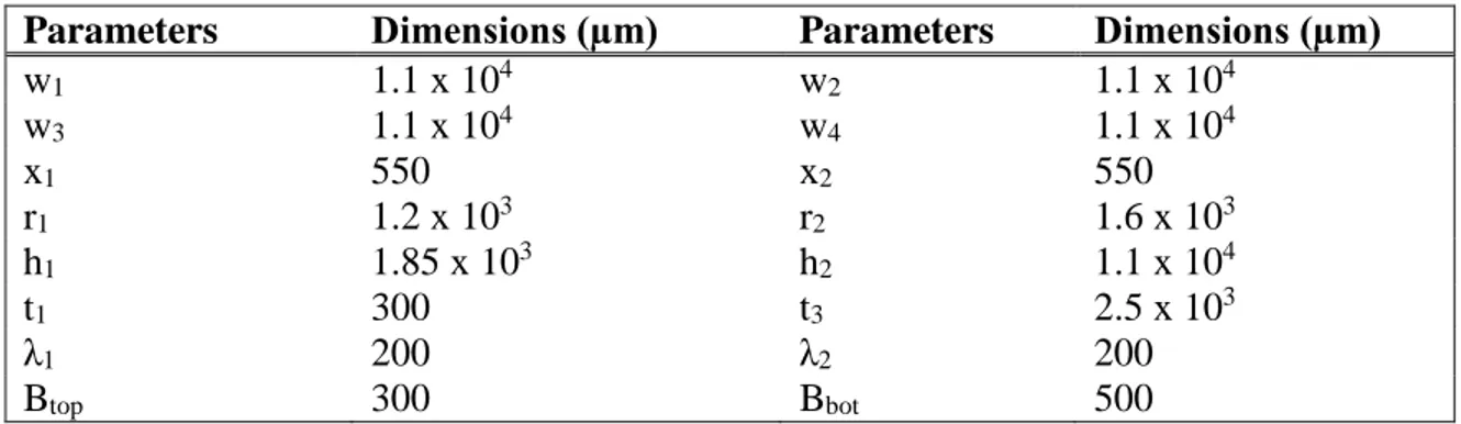
By using Finite-Element-Method, the simulation of the proposed design is completed to see bending behavior of the upper plate and change in ∆ (x, y). The results are shown in Figure 4.4. Mainly, in this process 2.8 kPa pressure is applied to center of the top plate surface and then a deflection of 3.77 µm is acquired. The process is completed by using COMSOL Multiphysics 5.0 software and the workspace is prepared in Structural Mechanics in COMSOL. Finite element is imported into Solid Mechanics as a choice of physic interface. After preparing the properties of the design work-space the study results are chosen as
Stationary Method to be illustration of result of the work.
For simulation, in the process of preparing the component features, some of the sub-work-titles are chosen as Definitions, Geometry, Materials, Solid Mechanics and Mesh. Firstly, whole geometry of the design which is prepared by using Solid Works software is converted to a step file format to be able to import it into the COMSOL software. After importing the required file, the whole structure is defined as Vero-Clear material to assign material properties to the geometry. The quantities of the imported properties can be seen in Figure 4.1.
Figure 4.1. Assigning the material properties. Vero Clear material properties and boundary load selection for left and right, respectively.
In the physic interface of Solid Mechanics, the five sub-part is prepared to edit according to the design. Linear Elastic Material expresses the gradient mechanical parameters to provide us aspects for mechanical outputs such as stress, displacement. Free can be used for assigning about moving properties of the design to separate which parts of the structure can move and which are not able. Initial Values is the opportunity of assigning the information about overridden and contributed parts of material which should be avoided as to be overridden for parts of design. Fixed Constraints has opposite relation with Free to express a choice of fixed boundaries which cannot be moved during all operation of simulation.
Boundary Load provide us to apply desired mechanical inputs which can be a pressure. For
proposed design, only the membrane is activated to apply a boundary load. The activation of the boundary load is illustrated in Figure 4.1.
In the next step, for meshing process, it is a crucial point of the COMSOL because the design cannot be simulated without doing a mesh process. In this simulation, the meshing application was complated by assigning the Free Tetrahedral to create equal randomness throughout the membrane surface. The dimensions of the object are considered while creating intervals as quantities for the object needs to be meshed. It is assigned as 0.0125 meters to 2.25 𝑥 10-6, shows maximum and minimum sizes, respectively. The interval of sizes' inputs and the other factors are illustrated below Figure 4.2.
Figure 4.2. Assigning the mesh parameters.
The duration of meshing varies according to amount of interval between maximum and minimum element size which is explained above. After the process, the finished illustration of the mesh is revealed below.
Figure 4.3. The meshed result of the proposed design.
The Study part of the COMSOL is one of the other main headings. It should be analyzed well after whole preparation that explained previous paragraphs are finished. As it explained above, by using COMSOL, the simulation of the mentioned design is completed to see the bending behavior of the upper plate and to see change in ∆ (x, y). The results are shown in Figure 4.4. 2.8 kPa pressure is applied to the center of the top plate surface for the simulations and a deflection of 3.77 µm is acquired after the process.
Figure 4.4. The total displacement of the top plate of recommended design under 2.8 kPa differential pressure. The central deflection of the plate is 3.77 micrometer at the vertical axis.
Besides the displacement results, also the x-axis load and the y-axis load that are caused by the 2.8 kPa pressure, are illustrated below as horizontal effects of the applied pressure in simulation.
Figure 4.5. The horizontal effects of the applied pressure.
The above study results of x-axis load and y-axis load shows us, while we are applying pressure into z direction, the observable x and y axis loads are said to be negligible.
5. FABRICATION OF THE 3D PRINTED CAPACITIVE PRESSURE
SENSOR
As it was explained in previous chapters, before the fabrication, all designing and simulation steps are completed. Then the design is manufactured and it is prepared for measurement part. In the section, fabrication process is discussed in three steps. Firstly, as a 3D printing method, the sub-section of 3D printing includes an explanation of the method that is additive manufacturing and it is revealed that how it can be used in subsequent processes. Then sputtering is reviewed by placing of the sputtering in physical vapor deposition. Lastly, the bonding process is discussed and final product is illustrated.
5.1. 3D PRINTING
In recent advances, additive manufacturing (AM) is one of the most known technique for rapid prototyping and well-shaping as well as it is commonly used in MEMS. The AM is a name that said to define such technologies which create an object by adding layer to layer of any available matter. In this technique, different type of methods and materials can be employed. One of the basic step for all kinds of AM methods is usage of computer by using a special type of software which are called Computer Aided Design (CAD). Creating a CAD file provides us to design a 3D objects for desired production. In the proposed design, the CAD file image is illustrated below Figure 5.1 that obtained by using Solid Works software.
With designing CAD file, AM device can reach the data by using another software that is used for 3D printing machine.
The AM device takes the sketch as a CAD file and begins to build a structure by adding layer on layer by using a consumable material. The consumable materials can be chosen as a plastic, some powder filaments, any liquids or sheet of paper.
Additionally, in the CAD software, it is important to save file as an assembly mode in order to have opportunity of using two or more materials in the 3D printing process. We have to use assembly mode in Solid Works to manufacture different parts by assigning two or more different materials with this addition. In the proposed design, a material that is Vero-Clear RGD 810 is used. The mechanical properties of this material listed below in Table 5.1.
Table 5.1. Material properties of the Vero-Clear RGD 810 [34].
Parameters Units Metric Units Imperial
Tensile strength MPa 50-65 psi 7250-9450
Elongation at break % 10-25 % 10-25
Modulus of Elasticity MPa 2000-3000 psi
290.000-435.000
Flexural Strength MPa 75-110 psi 11000-16000
Flexural Modulus MPa 2200-3200 psi
320.000-465.000
HDT @ 0.45MPa Celcius 45-50 Fahrenheit 113-122
HDT @ 1.82MPa Celcius 45-50 Fahrenheit 113-122
Izod Notched Impact J/m 23-30 ft lb/inch 0.375-0.562
Water Absorption % 1.1-1.5 % 1.1-1.5
Tg Celcius 52-54 Fahrenheit 126-129
Shore Hardness (D) Scale D 83-86 Scale D 83-86
Rockwell Hardness Scale M 73-76 Scale M 73-76
Polymerized Density g/cm3 1.04-1.05
Ash Content % 0.02-0.06 % 0.02-0.06
The name of Additive Manufacturing includes such technologies that are Rapid Prototyping (RP), Direct Digital Manufacturing and 3D printing. As it is elaborated, for 3D printing methods, there are lots of techniques that were developed to manufacture 3D objects. Some of the important names of the techniques are Stereolithography (SLA), Fused Deposition Modeling (FDM), Selective Laser Sintering (SLS), Digital Light Processing (DLP), Laminated Object Manufacturing (LOM), Selective Laser Melting (SLM) and Electronic Beam Melting (EBM).
For explaining the technique of fused deposition modeling (FDM) which is chosen as AM technique for the proposed design, the technology was developed by Scott Crump who is Stratasys LTD. founder, in the 1980s. The alternative 3D printing companies have adopted same kind technologies but with different names. For example, MakerBot uses almost same technology that is named as Fused Filament Fabrication (FFF).
With the method of FDM we can produce not only functional models but also concept prototypes and final end-use designs. One of the main advantages for FDM is all the printing process can be done in high-performance by using engineering grade thermoplastic so specifically, this feature can be beneficial for mechanical engineers as well. The main advantage of the FDM is high-grade thermoplastics which is used commonly so it can be employed with reliable mechanicals within the quality of high-grade thermal and chemical properties. A basic FDM process is illustrated below in Figure 5.2.
Figure 5.2. The basic illustration of a FDM manufacturing [50].
As seen in the Figure 5.2, the thermoplastic is built from bottom of the chamber with a thermoplastic consumable material then nozzle moves with a technique of layer-upon-layer until the object is finished. When a thin layer of thermoplastic is built downside of the chamber, it cools down and hardens.
During the process, a computer reads the data from CAD file as identifying the dimensions of the object in X, Y and Z axis and makes moving the nozzle to follow planned path.
It is another new fashion quality of FDM based 3D printer when printing is ended the support material can be solved with water, NaOH or snapping the support material off by hand if the object is not sensitive enough. Then, if the object shape need to be changed, it can be milled or painted, plated, deposited or lots of other fabrication steps of MEMS can be applied. The duration of printing depends on the size and complexity of objects.
However, the height of the design (size in Y) affects the duration more than the width of the design (size in X) due to the 3D printing device builds the objects as layer by layer through horizontal axis.
The proposed sensor is printed by using an Objet 260 Connex 3D printer which has FDM technique. Vero-Clear RGD810 polymer material is used as a consumable material [34]. The material properties of the used consumable material are given in Table 5.1. Also the print-out of the 3D printing process is illustrated below in Figure 5.3.
Figure 5.3. Print-out of the mentioned AM technique
As it can be seen above, the print-out of the design is prepared according to sinusoidal grid of equation (3.6). Sine and cosine functions of the equation indicates 90 degree of phase difference for each other. As it explained in previous paragraphs, the support material that
built by 3D printer allocated around of the plates can be removed with water, an appropriate chemical or snapping by hand if the design is not small or not sensitive.
In order to avoid problems, printed polymer sensor is strip-off from the support material by immersing it into a 40% NaOH solution for approximately 16 hours.
5.2. SPUTTERING
Following to previous fabrication step to establish a conductive surface and provide capability of the electrical connections, the sensor surfaces are coated with 10 nm thick chromium and 115 nm thick gold by using sputtering process, respectively. Sputtering is categorized as a method under Physical Vapor Deposition (PVD) technique that is recently employed in MEMS fabrication processes in todays' advances. Physical Vapor Deposition (PVD) is generally applied to deposit thin layers of material. By using this process, typically in the range of nanometers to micrometers can be deposited. PVD steps are an environmentally friendly technique that includes of these which are three fundamental steps [35-36]. Firstly, evaporation process is completed with the high temperature vacuum or generally, gaseous plasma. In the proposed design, evaporation of the chromium and gold are used by plasma Argon gaseous. Secondly, transportation of the evaporated material in vacuum chamber that can be categorized as partial vacuum chambers and exact vacuum chambers. Partial vacuum chamber means that there is no gaseous in the vacuum chamber except novel gasses in order to avoid oxidation as an undesired reaction. For all PVD techniques and in particular for the sputtering technique as PVD, the above explained steps are valid. Moreover, some specific points differ between sputtering and other alternatives. For an alternative PVD technique which is named as thermal evaporation, the main step is defined as vaporization of deposition material by giving heat to it with using similar kind of processes. However, in sputtering we need to use a plasma-assisted processes. The source target is evaporated by bombarding it with gaseous ions which is generally Argon. Beside of explains, it can be said to add more vapor deposition techniques such as Chemical Vapor Deposition or Atomic Layer Deposition.
5.3. IMPLEMENTED DEVICES
For creating an electrical connection for the sensor, copper wires are attached to the plates using silver epoxy. Generally, in the market, copper wire contacting that is named as copper wire bonding that is applied for connecting the semiconductors or passive circuit elements rather than gold and aluminum wires. The copper cables are also to be used conventionally in packaging services.
The reasons are first, to use of copper wire to reduce the cost up to 90% then it has usable electrical and thermal conductivity that are 58.5 𝑥 106 Siemens/m and 401 W/m.k, respectively. The electrical and thermal conductivities of copper metal make the copper more preffered than alternative usable metals. Moreover, for a metal, when the they are used in a bonding process, it might cause to grow some additional metal that may cause some disorientation because of the linear temperature expansion coefficient of metals. The expansion coefficient of copper is 16-16.7 𝑥010-6 m/(m K) which is more stable than aluminum, gold or most of the other metals. Higher thermal conductivity means, if a metal has higher thermal conductivity such as copper, it can easily dissipate the heat that is applied to itself, which means that copper cables can prevent the negative effects of the heat for the system. Therefore, copper cables are packaged to make the system more efficiently than the system that contains lower thermal conductivity metals. As a result, the higher thermal conductivity condition minimizes the thermal stress.
Furthermore, the copper wires are more reliable when it is used in high temperature operations because it has not only higher thermal conductivity but also higher mechanical stability than most of the alternative metals especially than gold and aluminum (excluding silver). Exception of the silver is also valid for the all above other explained properties. Therefore, silver epoxy is applied at end of the copper wire.
As known in the literature, normally, gold is 3 to 10 times more expensive than copper so if the gold metal is chosen instead of copper, this causes drastically cost increasing for a semiconductor packaging company. Another advantage for copper compared with gold is lower tendency for forming intermetallic compounds on the bond pads.
![Figure 2.1. Basic illustration a parallel plate capacitive sensor [6].](https://thumb-eu.123doks.com/thumbv2/9libnet/4277883.68804/15.894.283.672.656.801/figure-basic-illustration-a-parallel-plate-capacitive-sensor.webp)
![Figure 2.2. Basic illustration of parallel comb capacitive sensor [6].](https://thumb-eu.123doks.com/thumbv2/9libnet/4277883.68804/16.894.337.628.164.290/figure-basic-illustration-of-parallel-comb-capacitive-sensor.webp)
![Figure 2.4. Parylene-C polymer-based capacitive sensor [12].](https://thumb-eu.123doks.com/thumbv2/9libnet/4277883.68804/23.894.318.653.156.613/figure-parylene-c-polymer-based-capacitive-sensor.webp)
![Figure 2.5. PDMS polymer based shear and normal force sensor [13].](https://thumb-eu.123doks.com/thumbv2/9libnet/4277883.68804/26.894.281.676.142.515/figure-pdms-polymer-based-shear-normal-force-sensor.webp)
![Figure 2.6. Change in capacitances which caused by (a) tegafur, (b) uridine, (c) flurouracil, (d) uracil, (e) m- m-aminophenol, (f) ascorbic acid and (g) mercapto ethylamine [14]](https://thumb-eu.123doks.com/thumbv2/9libnet/4277883.68804/27.894.272.667.163.574/figure-capacitances-tegafur-flurouracil-aminophenol-ascorbic-mercapto-ethylamine.webp)
![Figure 2.7. The designed electronic structure is fixed to the polyphenyl sulfone (PPSF) that printed-out from a 3D printer [22]](https://thumb-eu.123doks.com/thumbv2/9libnet/4277883.68804/28.894.168.815.624.836/figure-designed-electronic-structure-polyphenyl-sulfone-printed-printer.webp)