5873
IOP PUBLISHING JOURNAL OF PHYSICS D: APPLIED PHYSICS
J. Phys. D: Appl. Phys. 40 (2007) 5873–5877 doi:10.1088/0022-3727/40/19/012
Resonant cavity based compact efficient
antireflection structures for photonic
crystals
Zhaofeng Li
1,2, Ekmel Ozbay
1, Haibo Chen
2, Jianjun Chen
2,
Fuhua Yang
2and Houzhi Zheng
21 Nanotechnology Research Center, Department of Physics, and Department of Electrical and
Electronics Engineering, Bilkent University, Bilkent, 06800 Ankara, Turkey
2 State Key Laboratory for Superlattices and Microstructures, Institute of Semiconductors, Chinese Academy of
Sciences, PO Box 912, Beijing 100083, People’s Republic of China E-mail: [email protected]
Received 24 June 2007, in final form 7 August 2007 Published 21 September 2007
Online at stacks.iop.org/JPhysD/40/5873
Abstract
We propose an effective admittance (EA) method to design antireflection structures for two-dimensional photonic crystals (PCs). We demonstrate that a compact and efficient antireflection structure, which is difficult to obtain by the conventional admittance matching method, can be readily designed by the EA method. The antireflection structure consists of an air slot resonant cavity that is constructed only with the materials that
constitute the PC. Compared with a bare PC, the reflection from a PC with an antireflection structure is reduced by two orders of magnitude over a wide bandwidth. To confirm the presented EA method, finite-difference time-domain (FDTD) simulations are performed, and the results from the FDTD and the EA method are in good agreement.
1. Introduction
One unique property of photonic crystals (PCs) [1, 2] is the unusual dispersion of the propagating Bloch modes. Many useful effects, such as the superprism effect [3], negative refraction [4,5], subwavelength focusing [6] and selfcollimation[7,8],
resultfromspecificfeaturesofthePCbands. All these applications require a negligibly small reflection loss at the PC interface, where light can be coupled efficiently in and out of the PC structure. This will prevent unwanted reflections that can cause interference and cross talk between devices within PC-based compact integrated optical circuits.
Several techniques have been proposed to reduce reflections. Baba and Ohsaki [9] calculated transmission efficiencies as high as 99.8% by employing projected air holes as the first layer of an air hole-type PC. However, the direction in which the holes are projected relative to the incident beam
is critical. As soon as the acceptance angle exceeds 3◦, the transmittance quickly reduces to values below 79%. Witzens
et al [10] proposed a kind of mode matching interface that consists of several cascaded diffraction gratings. After imposing constructive interference conditions between successive gratings, the reflections from individual gratings can be suppressed. Recently, White et al [11] reported high coupling efficiencies into rod-type PCs with unmodified interfaces under certain conditions. Nevertheless, this phenomenon does not exist in air hole-type PCs. Momeni and Adibi [12] presented an adiabatic matching stage for reflection reduction based on the principle of gradual change, which requires a multilayer matching stage in order to obtain high performance. In particular, Ushida et al [13] pointed out that an electromagnetic (EM) Bloch wave propagating in a PC can be characterized by the admittance (or impedance) of the wave. Based on the concept of admittance, they proposed a design of a very compact antireflection coating for a
infinite two-dimensional (2D) PC. However, the efficiency of the proposed design depends on the flatness of the spatial modulation of the impedance along the interface of the PC. If the flatness of the impedance is insufficient, it will be difficult to find a very efficient antireflection coating. Furthermore, the material of the antireflection coating is not one of the materials constituting the PC, and it might be difficult to find and use such a material with a certain refractive index. Consequently, a new approach is needed for the design
Z Li et al
of a compact antireflection structure for 2D PCs where the admittance greatly fluctuates along the interface of the PC. In this paper, we propose an effective admittance (EA) method to design a simple and compact antireflection structure with high efficiency. Although our method can be applied to both rod-type PCs and air hole-type PCs, we will restrict ourselves to 2D air hole-type PCs to demonstrate its validity.
In this paper, we first propose the EA method and obtain an effective refractive index for a PC interface. Based on this effective refractive index, we design a simple and compactantireflectionstructurewithhighefficiencyforthePC interface by the conventional transfer matrix method (TMM). The antireflection structure is constructed with the materials constituting the PC only. The above results are confirmed by finite-difference time-domain (FDTD) simulations.
2. The effective admittance method
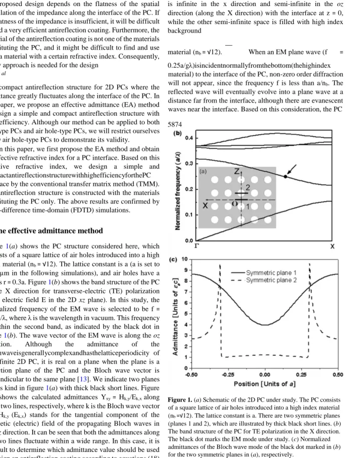
Figure 1(a) shows the PC structure considered here, which consists of a square lattice of air holes introduced into a high index material (nb = √12). The lattice constant is a (a is set to be 1 µm in the following simulations), and air holes have a radius r = 0.3a. Figure 1(b) shows the band structure of the PC in the X direction for transverse-electric (TE) polarization (with electric field E in the 2D xz plane). In this study, the normalized frequency of the EM wave is selected to be f = 0.25a/λ, where λ is the wavelength in vacuum. This frequency is within the second band, as indicated by the black dot in figure 1(b). The wave vector of the EM wave is along the oz direction. Although the admittance of the Blochwaveisgenerallycomplexandhasthelatticeperiodicity of an infinite 2D PC, it is real on a plane when the plane is a reflection plane of the PC and the Bloch wave vector is perpendicular to the same plane [13]. We indicate two planes of this kind in figure 1(a) with thick black short lines. Figure
1(c) shows the calculated admittances Yxy = Hk,y/Ek,x along these two lines, respectively, where k is the Bloch wave vector and Hk,y (Ek,x) stands for the tangential component of the magnetic (electric) field of the propagating Bloch waves in the oz direction. It can be seen that both the admittances along the two lines fluctuate within a wide range. In this case, it is difficult to determine which admittance value should be used to design an antireflection coating according to equations (18) and (19) in [13].
Tocircumventtheabovedifficulty, weintroduceaconcept ofEAforthesymmetricplane. Therearetwosymmetricplanes in figure 1(a), and we choose plane 1 to be the surface of the open PC considering the convenience of practical fabrication. Figure 2(a) shows a PC structure with an open surface that has
the same parameters as the PC shown in figure 1(a). The PC is infinite in the x direction and semi-infinite in the oz direction (along the X direction) with the interface at z = 0, while the other semi-infinite space is filled with high index background
material (nb = √12). When an EM plane wave (f = 0.25a/gλ)isincidentnormallyfromthebottom(thehighindex material) to the interface of the PC, non-zero order diffraction will not appear, since the frequency f is less than a/nb. The reflected wave will eventually evolve into a plane wave at a distance far from the interface, although there are evanescent waves near the interface. Based on this consideration, the PC 5874
Figure 1. (a) Schematic of the 2D PC under study. The PC consists
of a square lattice of air holes introduced into a high index material (nb =√12). The lattice constant is a. There are two symmetric planes
(planes 1 and 2), which are illustrated by thick black short lines. (b) The band structure of the PC for TE polarization in the X direction. The black dot marks the EM mode under study. (c) Normalized admittances of the Bloch wave mode of the black dot marked in (b) for the two symmetric planes in (a), respectively.
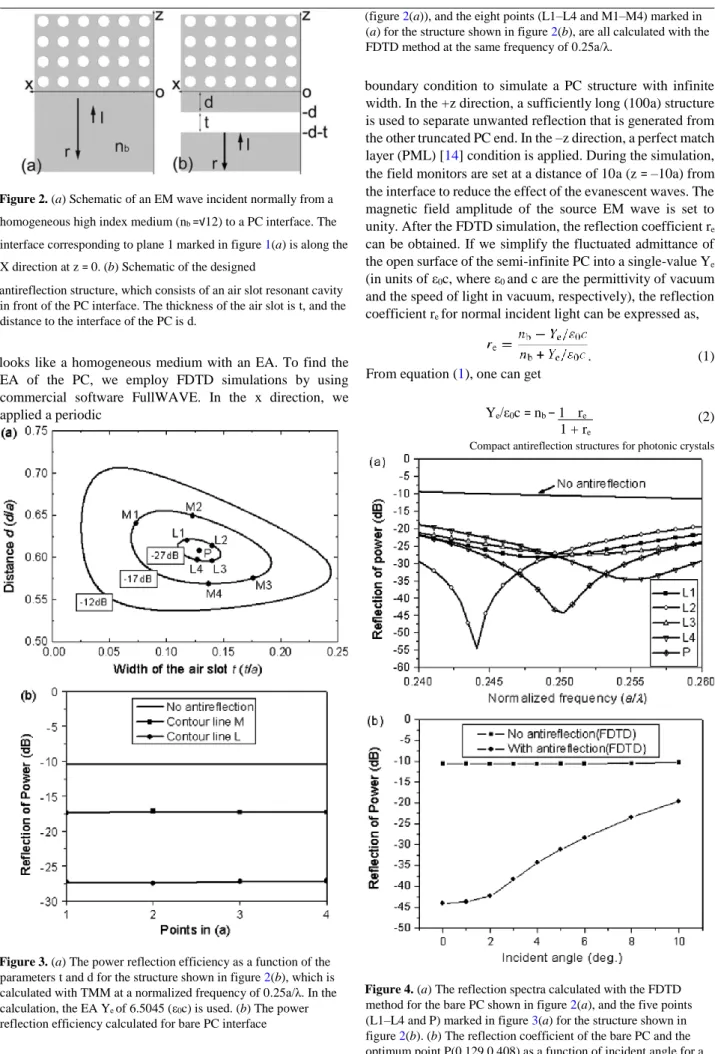
5875 Figure 2. (a) Schematic of an EM wave incident normally from a
homogeneous high index medium (nb =√12) to a PC interface. The
interface corresponding to plane 1 marked in figure 1(a) is along the X direction at z = 0. (b) Schematic of the designed
antireflection structure, which consists of an air slot resonant cavity in front of the PC interface. The thickness of the air slot is t, and the distance to the interface of the PC is d.
looks like a homogeneous medium with an EA. To find the EA of the PC, we employ FDTD simulations by using commercial software FullWAVE. In the x direction, we applied a periodic
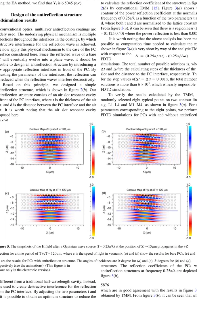
Figure 3. (a) The power reflection efficiency as a function of the
parameters t and d for the structure shown in figure 2(b), which is calculated with TMM at a normalized frequency of 0.25a/λ. In the calculation, the EA Ye of 6.5045 (ε0c) is used. (b) The power
reflection efficiency calculated for bare PC interface
(figure 2(a)), and the eight points (L1–L4 and M1–M4) marked in (a) for the structure shown in figure 2(b), are all calculated with the FDTD method at the same frequency of 0.25a/λ.
boundary condition to simulate a PC structure with infinite width. In the +z direction, a sufficiently long (100a) structure is used to separate unwanted reflection that is generated from the other truncated PC end. In the –z direction, a perfect match layer (PML) [14] condition is applied. During the simulation, the field monitors are set at a distance of 10a (z = –10a) from the interface to reduce the effect of the evanescent waves. The magnetic field amplitude of the source EM wave is set to unity. After the FDTD simulation, the reflection coefficient re can be obtained. If we simplify the fluctuated admittance of the open surface of the semi-infinite PC into a single-value Ye (in units of ε0c, where ε0 and c are the permittivity of vacuum and the speed of light in vacuum, respectively), the reflection coefficient re for normal incident light can be expressed as,
. (1)
From equation (1), one can get
Ye/ε0c = nb − 1 re 1 + re
(2) Compact antireflection structures for photonic crystals
Figure 4. (a) The reflection spectra calculated with the FDTD
method for the bare PC shown in figure 2(a), and the five points (L1–L4 and P) marked in figure 3(a) for the structure shown in figure 2(b). (b) The reflection coefficient of the bare PC and the optimum point P(0.129,0.408) as a function of incident angle for a normalized frequency of 0.25a/λ.
We call the above method the EA method in this study. By using the EA method, we find that Ye is 6.5045 (ε0c).
3. Design of the antireflection structure andsimulation results
In conventional optics, multilayer antireflection coatings are widely used. The underlying physical mechanism is multiple reflections throughout the interfaces in the coatings, by which destructive interference for the reflection wave is achieved. We now apply this physical mechanism to the case of the PC interface considered here. Since the reflected wave of a bare PC will eventually evolve into a plane wave, it should be feasible to design an antireflection structure by introducing a few appropriate reflection interfaces in front of the PC. By adjusting the parameters of the interfaces, the reflection can be reduced when the reflection waves interfere destructively. Based on this principle, we designed a simple antireflection structure, which is shown in figure 2(b). Our antireflection structure consists of an air slot resonant cavity in front of the PC interface, where t is the thickness of the air slot, and d is the distance between the PC interface and the air slot. It is worth noting that the air slot resonant cavity proposed here
respectively (see the animations). (This figure is in colour only in the electronic version)
is different from a traditional half-wavelength cavity. Instead, it is used to create destructive interference for the reflection from the PC interface. By adjusting the two parameters t and d, it is possible to obtain an optimum structure to reduce the
reflection. Utilizing the EA Ye obtained in section 2, it is easy to calculate the reflection coefficient of the structure in figure
2(b) by conventional TMM [15]. Figure 3(a) shows the contour of the power reflection coefficient at the normalized frequency of 0.25a/λ as a function of the two parameters t and d, where both t and d are normalized to the lattice constant a. From figure 3(a), it can be seen that there is a region near (t,d) = (0.125,0.40) where the power reflection is less than 0.002.
It is worth noting that the above analysis has been made possible as computation time needed to calculate the map shown in figure 3(a) is very short by way of the analytic TMM with respect to the
FDTD
simulations. The total number of possible solutions is, where are the calculating steps of the thickness of the air slot and the distance to the PC interface, respectively. Thus, for the step values of , the total number of solutions is more than 6 × 10⁵, which is nearly impossible for FDTD simulation.
To verify the results calculated by the TMM, we randomly selected eight typical points on two contour lines, e.g. L1–L4 and M1–M4, as shown in figure 3(a). For the parameters corresponding to the eight points, we performed FDTD simulations for PCs with and without antireflection
structures. The reflection coefficients of the PCs with antireflection structures at frequency 0.25a/λ are depicted in figure 3(b),
5876
which are in good agreement with the results in figure 3(a) obtained by TMM. From figure 3(b), it can be seen that when Z Li et al
Figure 5. The snapshots of the H field after a Gaussian wave source (f = 0.25a/λ) at the position of Z =−15µm propagates in the +Z direction for a time period of T (cT = 120µm, where c is the speed of light in vacuum). (a) and (b) show the results for bare PCs. (c) and (d) are the results for PCs with antireflection structure. The angles of incidence are 0◦ degree for (a) and (c), 3◦ degrees for (b) and (d),
5877 the parameters (t,d) fall on the contour line L, the power
reflection is reduced by nearly two orders of magnitude compared with the bare PC interface. Nevertheless, the above results are not meant for optimum antireflection structures.
We now investigate the frequency dependence of the reflectance from PCs with and without resonant cavities. We calculated the reflection spectra of five points, P and L1–L4, together with a bare PC, as shown in figure 4(a). Firstly, from the reflection spectra of point P, one sees that within the frequency range 0.24–0.26 a/λ, the reflection is reduced by more than one order of magnitude. Especially in the frequency range from 0.246 to 0.254 a/λ, the reflection is even reduced by more than two orders of magnitude compared with the bare PC. Furthermore, from the reflection spectra of L1–L4, it can be seen that although their parameters (t,d) differ fromtheoptimumparameterP(0.129,0.408)byapproximately (±0.01,±0.01), the reflection can still be reduced by more than five times within a wide frequency range 0.24–0.26 a/λ compared with the bare PC.
Toevaluatethesensitivityoftheantireflectionefficiencyto the incident angle, we also calculated the reflection at different incident angles from 0◦ to 10◦ by FDTD simulations. In our simulations, the PML [14] boundary condition was applied to all the boundaries, and a Gaussian beam with a full width at half maximum (FWHM) of w = 10a was used as the source wave. A sufficiently large (50a × 50a) structure was used to separate unwanted reflections. Figure 4(b) shows the power reflection coefficients of point P(0.129, 0.408) as a function of the incident angle for a normalized frequency of 0.25a/λ. It can be seen that the reflection from the PC (with a resonant cavity) increases minimally with the rise of the incident angle. Consequently, for incident angles within ±5◦, the reflection coefficient still remains less than that of the bare PC by nearly two orders of magnitude.
In order to demonstrate the effect of the air slot more clearly, we performed FDTD simulations for the optimum point P with parameters (t,d) = (0.129,0.408) with a Gaussian wave source incident to a bare PC and a PC with antireflection structure. In the simulations, the Gaussian beam has a frequency of 0.25a/λ with a FWHM of 5a, and the angles of incidence are selected to be 0◦ and 3◦. Figure 5 shows the snapshot of the H field after the propagation of the wave approaches steady. From figures 5(a) and (b), the reflection from the surface of the bare PC can be clearly seen, whereas from figures 5(c) and (d), almost no reflection can be seen. Besides, it can be seen that very little deformation is introduced to the profile of the propagating wave. By comparing the results for the bare PC and the PC with antireflection structure, the high efficiency of the antireflection structure is seen intuitively.
In order to verify the feasibility of the EA method and the air slot resonant cavity antireflection structures, we also designed antireflection interfaces for triangular lattice PCs. The results are similar to those of square lattice PCs presented here. Furthermore, considering that the applications of PCs are mainly based on PC slabs, we also applied the air slot resonant cavity antireflection structure to square lattice PC slabs. Our preliminary results show that the antireflection structure can indeed reduce the reflection and increase the transmission, while at the same time it has little effect on the
out-of-planescatteringlosses. Moreinvestigationsconcerning antireflection in PC slabs are currently in progress.
4. Conclusions
In summary, we used the EA method to design a simple and compact antireflection structure for 2D PCs. The antireflection structure consists of a simple air slot resonant cavity. When compared with a bare PC, the reflection Compact antireflection structures for photonic crystals from a PC with an antireflection structure is reduced by two orders of magnitude over a wide bandwidth. The antireflection structure also works quite efficiently within a certain incident anglerange. Theproposedresonantcavitybasedantireflection structures can bring a significant advantage for PC based compact integrated optical circuits.
Acknowledgments
This work is supported by the special fund for Major State Basic Research Project No. 2001CB309302 of China. This work is also supported by the European Union under the
projects EU-NoE-METAMORPHOSE,
EU-NoEPHOREMOST and TUBITAK under Project Nos. 104E090, 105E066, 105A005 and 106A017. One of the authors (EO) also acknowledges partial support from the Turkish Academy of Sciences.
References
[1] Yablonovitch E 1987 Phys. Rev. Lett. 58 2059
[2] Joannopoulos J D, Meade R D and Winn J N 1995 Photonic
Crystals: Molding the Flow of Light (Princeton, NJ:
Princeton University Press)
[3] Kosaka H, Kawashima T, Tomita A, Notomi M, Tamamura T, Sato T and Kawakami S 1999 Appl. Phys. Lett. 74 1370
[4] Notomi M 2000 Phys. Rev. B 62 10696
[5] Cubukcu E, Aydin K, Ozbay E, Foteinopolou S and Soukoulis C M 2003 Nature 423 604
[6] Cubukcu E, Aydin K, Ozbay E, Foteinopolou S and Soukoulis C M 2003 Phys. Rev. Lett. 91 207401 [7] Prather D W, Shi S, Pustai D M, Chen C, Venkataraman S, Sharkawy A, Schneider G J and Murakowski J 2004 Opt.
Lett. 29 50
[8] Yu X and Fan S 2003 Appl. Phys. Lett. 83 3251
[9] Baba T and Ohsaki D 2001 Japan. J. Appl. Phys. 40 5920
[10] Witzens J, Hochberg M, Baehr-Jones T and Scherer A 2004
Phys. Rev. E 69 046609
[11] White T P, Martijn de Sterke C, McPhedran P C and Botten L C 2005 Appl. Phys. Lett. 87 111107
[12] Momeni B and Adibi A 2005 Appl. Phys. Lett. 87 171104
[13] Ushida J, Tokushima M, Shirane M, Gomyo A and Yamada H 2003 Phys. Rev. B 68 155115
[14] Berenger J P 1994 J. Comput. Phys. 114 185