Active region dimensionality and quantum efficiencies of InGaN LEDs
from temperature dependent photoluminescence transients
Nuri Can,
1,2Serdal Okur,
1Morteza Monavarian,
1Fan Zhang,
1Vitaliy Avrutin,
1Hadis Morkoç,
1Ali
Teke,
2and Ümit Özgür
1,*1
Department of Electrical and Computer Engineering, Virginia Commonwealth University,
Richmond, VA 23284, USA
2
Physics Department, Balikesir University, Balikesir, 10145, Turkey
*E-mail: [email protected]
ABSTRACT
Temperature dependent recombination dynamics in c-plane InGaN light emitting diodes (LEDs) with different well thicknesses, 1.5, 2, and 3 nm, were investigated to determine the active region dimensionality and its effect on the internal quantum efficiencies. It was confirmed for all LEDs that the photoluminescence (PL) transients are governed by radiative recombination at low temperatures while nonradiative recombination dominates at room temperature. At photoexcited carrier densities of 3 – 4.5 x 1016 cm-3 , the room-temperature Shockley-Read-Hall (A) and the bimolecular
(B) recombination coefficients (A, B) were deduced to be (9.2x10⁷ s-1, 8.8x10⁻¹⁰ cm3s-1), (8.5x10⁷ s-1, 6.6x10⁻¹⁰ cm3s-1),
and (6.5x10⁷ s-1, 1.4x10⁻¹⁰ cm3s-1) for the six period 1.5, 2, and 3 nm well-width LEDs, respectively. From the
temperature dependence of the radiative lifetimes, τrad α TN/2, the dimensionality N of the active region was found to
decrease consistently with decreasing well width. The 3 nm wide wells exhibited ~T1.5 dependence, suggesting a
three-dimensional nature, whereas the 1.5 nm wells were confirmed to be two-three-dimensional (~T1) and the 2 nm wells close to
being two-dimensional. We demonstrate that a combination of temperature dependent PL and time-resolved PL techniques can be used to evaluate the dimensionality as well as the quantum efficiencies of the LED active regions for a better understanding of the relationship between active-region design and the efficiency limiting processes in InGaN LEDs.
Keywords: InGaN, light emitting diodes, time-resolved photoluminescence, recombination dynamics, quantum
1. INTRODUCTION
Over the past two decades, InGaN-based light emitting diodes (LEDs) have been extensively investigated for their widespread use in general lighting and full color displays. Solid-state lighting is environment friendly and offers significant energy savings and long operation lifetime.1 However, the requisite InGaN LEDs still exhibit efficiencies
below the theoretical limits and suffer from efficiency degradation at high injection.2 Although there is agreement on the
need for improved p-type conductivity in GaN to reduce the doping asymmetry, the optimum active region structure that would support the highest external quantum efficiency is still actively debated. While quantum wells provide superior carrier confinement, relatively thick wells (or double heterostructures) offer larger recombination volume and light output. Moreover, in the presence of the polarization fields, dimensionality of the active region determines the radiative recombination rate, and therefore, the quantum efficiency.3 In c-plane InGaN/GaN LEDs, the radiative lifetimes in
thicker wells are longer due to reduced overlap of electron and hole wave functions resulting from the large polarization field.4 Liu et al.5 reported room-temperature radiative decay times as long as 686 ns in high-In-content InGaN/GaN
LEDs with 3 nm thick wells, which accordingly exhibited relatively low internal quantum efficiencies (IQEs) of ~11%. Sasaki et al.6 also reported long radiative decay times of 168 ns and 242 ns for In
0.23Ga0.77N/GaN LEDs with 1.5 and 2.5
nm well thickness at room temperature, respectively, which were attributed to the localization of excitons due to In inhomogeneities.
Insight into the active region dimensionality and the IQE can be gained from the temperature dependence of the recombination rates that can be measured using time-resolved photoluminescence (TRPL) spectroscopy. Excitons confined in two dimensional (2D) states in quantum wells exhibit radiative decay times that increase linearly with temperature (T). In three dimensional (3D) structures, however, the radiative decay time follows T1.5 dependence.7
In this work, we investigated In0.15Ga0.85N/GaN LEDs with active regions composed of 6-period 1.5, 2, and 3 nm thick
wells by means of temperature dependent PL and TRPL. The temperature dependence of radiative decay times showed a
TN/2 dependence with N = 2 for LEDs having 1.5 or 2 nm thick wells and N = 3 for those with 3 nm wells. In addition,
temperature dependent IQEs calculated using the radiative and nonradiative decay times revealed two-fold enhancement for LEDs with 1.5 nm and 2 nm wells compared to that with 3 nm wells.
2. EXPERIMENTAL DETAILS
The c-plane InGaN/GaN LED structures were grown on ~4 µm thick n-GaN templates on sapphire in a vertical low-pressure metalorganic chemical vapor deposition (MOCVD) system, using trimethylgallium (TMG) and triethylgallium (TEG) as precursors for Ga, and trimethylindium (TMI), biscyclopentadienylmagnesium (Cp2Mg), NH3, and SiH4 as
precursors for Indium, Mg, N, and Si, respectively. The active regions are composed of 6 period (hexa) 1.5, 2, or 3 nm In0.15Ga0.85N wells separated by 3 nm thick In0.06Ga0.94N relatively low energy barriers to enhance hole transport across
the active regions. All LEDs incorporate electron injector layers to reduce the electron overflow:8 two-step staircase
electron injector (SEI) (5 nm In0.04Ga0.96N and 5 nm In0.08Ga0.92N grown on the given order) for the LED with 3 nm wells
and a 21 nm thick step-graded electron injector (In content graded from 4% to 10%) for the LEDs with 1.5 and 2 nm wells. A 60 nm thick Si doped (2x1018 cm-3) In
0.01Ga0.99N underlying layer was grown beneath the electron injector for
improvement of active region material quality. The LED structures were completed with 100 nm thick Mg doped p-GaN layers having 6x1017 cm-3 hole density, determined from Hall measurements in separate calibration samples. For devices,
square mesa patterns (400x400 µm2) were formed by conventional photolithography and chlorine-based inductively
coupled plasma (ICP) etching. Ti/Al/Ni/Au (30/100/40/50 nm) metallization annealed at 800 ºC for 60 s was used for n-type Ohmic contacts, and 5 nm/5nm Ni/Au electrodes served as the semi-transparent p-contacts. Finally, 40/50 nm Ni/Au electrodes were deposited on part of the mesa tops for p-contact pads.
TRPL measurements were performed using 380 nm wavelength excitation, which ensures photogeneration of carriers only in the active region, from a frequency-doubled Ti:Sapphire laser with 100 fs pulse width and 10 MHz repetition rate. The photoexcited carrier density was kept in the range of 3 – 4.5 x 1016 cm-3 assuming an absorption coefficient of
1x105 cm-2 in the In
0.15Ga0.85N active region. The excitation spot size on the sample surface was 50 µm in diameter. The
emitted light was collected using an optical fiber with the sample mounted in a variable-temperature closed-cycle He cryostat and focused into a spectrometer attached to a 30 ps resolution Hamamatsu streak camera. The TRPL curves were recorded by means of time-correlated photon counting mode.
3. RESULTS AND DISCUSSION
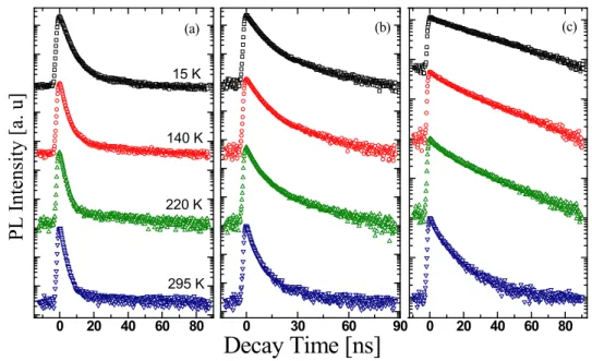
In order to investigate the recombination dynamics in hexa 1.5, 2, and 3nm LEDs, we performed TRPL measurements in
a temperature range of 15 – 300 K (see Figure 1). A biexponential decay function 1 2
1 2
t t
transients, where time constants τ1 and τ2 represent the fast and the slow decay components, respectively. The amplitudes
of the fast decay components were negligible compared to those of the slow decays (A1 << A2) for all PL transients;
therefore, the slow decay is representative of the PL lifetime and also indicative of exciton localization due to compositional inhomogeneities. As seen from Figure 1, the LED with 3 nm wells exhibits slower PL decay (13.9 ns) compared to those with 1.5 nm (7.2 ns) and 2 nm (8.6 ns) wells at room temperature (295 K). The increase in decay time with increasing well width is attributed to the polarization field-induced quantum confinement Stark effect,9,10 which
reduces the overlap of electron and hole wavefunctions and also results in redshift of the emission. Moreover, thicker wells might lead to larger In compositional fluctuations and the resulting trap levels may further increase the decay times.11 Due mostly to reduction of nonradiative recombination with reducing temperature, PL decay times are longer at
lower temperatures, reaching 14.2 ns, 16.6 ns, and 34.6 ns at 15 K for the LEDs with 1.5, 2, and 3 nm wells, respectively (see Figure 1).
0 20 40 60 80 0 30 60 90 0 20 40 60 80 295 K 220 K 140 K
P
L
Intensity [a. u]
(a) 15 KDecay Time [ns]
(b) (c)Figure 1. Temperature evolution of the PL transients for the hexa (a) 1.5 nm, (b) 2 nm, (c) 3 nm LED structures
.
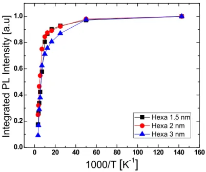
To extract the radiative and nonradiative decay times, several approaches have been adopted.12,13 The common
assumption made is that nonradiative recombination is much slower than the radiative one at very low temperatures, i.e. PL efficiency is about 100% at temperatures near and below 15 K. The measured PL intensity, I(T), is then given by the ratio of radiative recombination rate to the total recombination rate multiplied by the PL intensity at 15 K:
( )
(
15
)
1
1
1
1
1
r r r nr nrI T
I
K
τ
τ
τ
τ
τ
=
=
+
+
,
(1)
where τr and τnr are the temperature dependent radiative and nonradiative decay times, respectively. The quenching of PL
intensity shown in Figure 2, which is typical for nitride semiconductors, is caused by thermal activation of nonradiative recombination channels due to carrier delocalization.
0 20 40 60 80 100 120 140 160 0.0 0.2 0.4 0.6 0.8 1.0
Integrated PL Intensity [a.u]
1000/T
[
K
-1]
Hexa 1.5 nm Hexa 2 nm Hexa 3 nm
Figure 2. Arrhenius plots of temperature dependent integrated PL intensity for hexa 1.5, 2, and 3 nm LEDs.
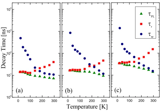
The PL decay time (τPL) obtained from exponential fits to transients is expressed in terms of radiative and nonradiative
decay times as
1
1
1
PL r nr
τ
=
τ
+
τ
.
(2)
Using equations (1) and (2) temperature dependent radiative and nonradiative decay times were extracted from the experimental data. As shown in Figure 3, radiative recombination is the dominant process at low temperature. Up to 100 K radiative decay time is almost independent of temperature for the LEDs with 1.5 and 2 nm wells, meaning that it is determined by the contribution from bound and localized excitons while nonradiative recombination plays only a minor
role.14 The carriers are thermally activated and reach defects where they can recombine nonradiatively above 100 K for
all the LEDs under investigation.
0 100 200 300 100 101 102 103 104 0 100 200 300 0 100 200 300
D
ecay Time [ns]
(a)
(c)
τ
PLτ
rτ
nrTemperature [K]
(b)
Figure 3. PL (τPL), radiative (τr) and nonradiative (τnr) decay times for hexa (a) 1.5 nm, (b) 2 nm, and (c) 3 nm LEDs as a function of
temperature.
The temperature at which the nonradiative recombination rate starts to exceed the radiative recombination rate, is almost the same for all three LEDs studied. The extracted radiative decay times at room temperature are 40 ns, 47 ns and 152 ns for the hexa 1.5, 2, and 3 nm LED structures, respectively. The increase in radiative decay time with increasing temperature could be attributed to carrier delocalization as well as reduced Coulombic interaction and the associated decrease in transition oscillator strength.
The temperature dependent radiative recombination rate, R(T) = 1/τr, is proportional to the relative number of excitons
with wavevectors in the light cone (wave vectors smaller thanE h ):c 15
( )
2 2 0 2 2 0exp
2 ( )
1
exp
2 ( )
E c N B N r Bk
d k
M k k T
R T
τ
k
d k
M k k T
∞⎛
⎞
−
⎜
⎟
⎝
⎠
=
∝
⎛
⎞
−
⎜
⎟
⎝
⎠
∫
∫
hh
h
,
(3)where d kN is the differential volume in k space,
h
is the Planck constant, kB is the Boltzmann constant, and M(k) is theexciton effective mass. Here, N shows the dimensionality of the material, which is N = 0 for a quantum dot, N = 1 for a quantum wire, N = 2 for a quantum well, and N = 3 for bulk material. For an N dimensional system, the radiative decay time can be expressed as:
2 0
N r
τ
=
τ T
,
(4)where τ0 is a characteristic constant.
Figure 4 shows the temperature dependence of the radiative decay time in logarithmic scale. The slopes of the radiative decay times obtained from fits using equation (4) provide dimensionality, N, of 2, ~2 and 3 for the LED structures with well widths of 1.5, 2, and 3 nm, respectively. These values suggest that the LED with 1.5 nm wells exhibits ideal quantum well behavior and that with 3 nm wells behaves like bulk, while that with 2 nm wells is close to being two-dimensional. These results are consistent with the reports that, due to the large effective electron mass of nitrides, quantum confinement is observed only when the well thickness of InGaN/GaN structures is less than 3 nm.16,17
10
100
10
110
2 slope=∼1 Hexa 3 nm Hexa 2 nm Hexa 1.5 nmτ
r[ns]
Temperature [K]
slope=1.5 slope=1Using the radiative and nonradiative recombination times extracted above, we also calculated the values of IQE, which is defined by 2 2
1
1
1
1
r nrBn
IQE
A
τ
An Bn
Bn
τ
=
=
=
+
+
+
,
(5)
where
A
=
τ
nr−1 is the Shockley-Read-Hall (SRH) nonradiative recombination coefficient, B =( )
nτr −1 is the bimolecular radiative recombination coefficient, and n is the carrier concentration. It was assumed that the Auger recombination coefficient C is negligible within the range of photogenerated carrier densities used here (3 – 4.5 x 1016cm-3).18
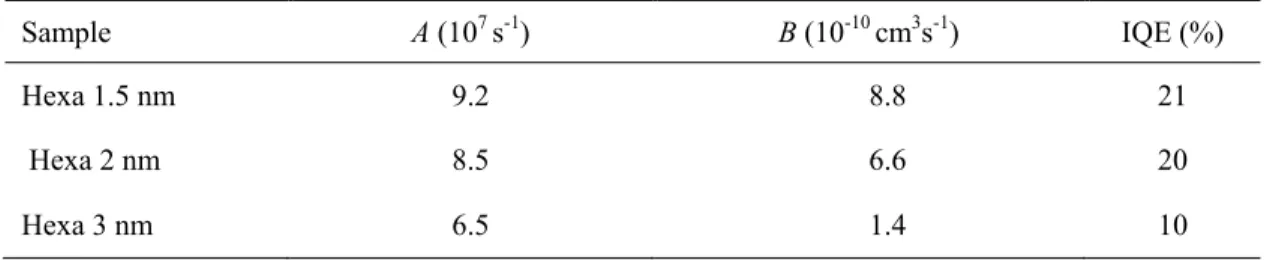
Table 1. Room temperature recombination coefficients and IQE values for the LED structures investigated here.
Sample A (107 s-1) B (10-10 cm3s-1) IQE (%)
Hexa 1.5 nm 9.2 8.8 21
Hexa 2 nm 8.5 6.6 20
Hexa 3 nm 6.5 1.4 10
Table I summarizes the recombination coefficients and the IQE values deduced for hexa LEDs with 1.5 nm, 2 nm and 3nm wells. Although the LED with 3 nm wells has the lowest A coefficient it also has the lowest B coefficient by far, and therefore, exhibits two times lower IQE than the LEDs with 1.5 nm and 2 nm wells. The smaller B coefficient in the wider well is likely due to larger separation of electron and hole wavefunctions by the internal polarization fields. All A and B coefficients obtained here are within the ranges reported for InGaN/GaN LED structures.19,20
In summary, temperature dependent TRPL experiments were carried out to investigate the optical properties of the hexa 1.5, 2 and 3 nm LED structures. Our data confirmed that radiative recombination rate decreases with increasing well width, which leads to lower IQE. The LEDs with 1.5 and 2 nm wells were found to exhibit two-dimensional behavior
and twice higher IQE compared to that with 3 nm wells, which was confirmed to exhibit three-dimensional bulk behavior.
4. ACKNOWLEDGMENTS
Nuri Can acknowledges the Ph.D. grant support from the scientific and technological research council of Turkey (TUBITAK). This work was partially supported by National Science Foundation (grant number EPMD 1128489).
5. REFERENCES
[1] H. Morkoç, Handbook of Nitride Semiconductors and Devices, Volume 3, Wiley-VCH, Chap. 1., (2008)
[2] V. Avrutin, S. A. Hafiz, F. Zhang, Ü. Özgür, E. Bellotti, F. Bertazzi, M. Goano, A. Matulionis, A. T. Roberts, H. O. Everitt, H. Morkoç, “Saga of efficiency degradation at high injection in InGaN light emitting diodes”, Turk J Phys., 38, 269 (2014)
[3] M. B. Nardelli, K. Rapcewicz, and J. Bernholc, "Polarization field effects on the electron-hole recombination dynamics in In0.2Ga0.8N/In1−xGaxN multiple quantum wells", Appl. Phys. Lett. 71 (21), 3135 (1997).
[4] P. Lefebvre, J. Allegre, B. Gil, H. Mathieu, N. Grandjean, M. Leroux, J. Massies, and P. Bigenwald, "Time-resolved photoluminescence as a probe of internal electic fields in GaN-(GaAl)N quantum wells", Phys. Rev B 59 (23), 15363 (1999).
[5] L. Liu, L. Wang, N. Y. Liu, W. Yang, D. Li, W. H. Chen, Z. C. Feng, Y. C. Lee, I. Ferguson, and X. D. Hu, " Investigation of the light emission properties and carrier dynamics in dual-wavelength InGaN/GaN multiple-quantum well light emitting diodes", Journal of Applied Physics 112 (8) 083101, (2012).
[6] A. Sasaki, K. Nishizuka, T. Wang, S. Sakai, A. Kaneta, Y. Kawakami, and S. Fujita, "Radiative carrier recombination dependent on temperature and well width of InGaN/GaN single quantum well", Solid State Communications 129 (1), 31 (2004).
[7] Y. Narukawa, Y. Kawakami, S. Fujita, S. Nakamura, “Dimensionality of excitons in laser-diode structures composed of InxGa1-xN multiple quantum wells”, Phys. Rev. B 59, 10283 (1999).
[8] F. Zhang, X. Li, S. Hafiz, S. Okur, V. Avrutin, Ü. Özgür, H Morkoç, A. Matulionis, “The effect of stair case electron injector design on electron overflow in InGaN light emitting diodes”, Appl. Phys. Lett. 103, 051122, (2013).
[9] T. Kuroda, A. Tackeuchi, “Influence of free carrier screening on the luminescence energy shift and carrier lifetime of InGaN quantum wells”, J. Appl. Phys. 92, 3071 (2002).
[10] S. W. Feng, Y. C. Cheng, Y. Y. Chung, C. C. Yang, Y. S. Lin, C. Hsu, K. J. Ma, J. I. Chyi, “Impact of localized states on the recombination in InGaN/GaN quantum well structures”, J. Appl. Phys. 92, 4441 (2002).
[11] T. S. Ko, T. C. Lu, T. C. Wang, M. H. Lo, J. R. Chen, R. C. Gao, H. C. Kuo, S. C. Wang, and J. L. Shen, "Optical characteristics of a-plane InGaN/GaN multiple quantum wells with different well widths", Appl. Phys. Lett. 90 (18), 181122, (2007).
[12] H. Kim, D. S. Shin, H. Y. Ryu, and J. I. Shim, "Analysis of Time-resolved Photoluminescence of InGaN Quantum Wells Using the Carrier Rate Equation", Japanese Journal of Applied Physics 49 (11), 112402, (2010).
[13] S. Chichibu, T. Onuma, T. Sota, S. P. DenBaars, S. Nakamura, T. Kitamura, Y. Ishida, and H. Okumura, "Influence of InN mole franction on the recombination processes of localized excitons in strained cubic InxGa1-xN/GaN multiple
[14] E. Berkowicz, D. Gershoni, G. Bahir, E. Lakin, D. Shilo, E. Zolotoyabko, A. C. Abare, S. P. Denbaars, and L. A. Coldren, "Measured and calculated radiative lifetime and optical absorbtion of InxGa1-xN/GaN quantum structures",
Physical Review B 61 (16), 10994 (2000).
[15] L. C. Andreani, Confined Electrons and Photons. (NATO ASI Series, Plenum Press - New York and London,), p.57, (1995).
[16] S. Keller, B. P. Keller, D. Kapolnek, A. C. Abare, H. Masui, L. A. Coldren, U. K. Mishra, and S. P. DenBaars, "Growth and characterization of bulk InGaN films and quantum wells", Appl. Phys. Lett. 68 (22), 3147 (1996).
[17] P. Blood, "On the dimensionality of optical absorption, gain, and recombination in quantum-confined structures", IEEE Journal of Quantum Electronics 36 (3), 354 (2000).
[18] X. Ni, X. Li, J. Lee, S. Liu, V. Avrutin, A. Matulionis, Ü. Özgür, and H. Morkoç, "Pivotal role of ballistic and quasi-ballistic electrons on LED efficiency", Superlattices and Microstructures 48 (2), 133 (2010).
[19] Q. Dai, M. F. Schubert, M. H. Kim, J. K. Kim, E. F. Schubert, D. D. Koleske, M. H. Crawford, S. R. Lee, A. J. Fischer, G. Thaler, and M. A. Banas, "Internal quantum efficiency and nonradiative recombination coefficient of GaInN/GaN multiple quantum wells with different dislocation densities", Appl. Phys. Lett. 94 (11), 111109, (2009). [20] Ü. Özgür, H. Liu, X. Li, X. Ni, H. Morkoç, “GaN-Based Light-Emitting Diodes: Efficiency at High Injection Levels”, Proceeding of the IEEE, 98, 1180 (2010).