High-speed GaAs-based resonant-cavity-enhanced 1.3 μm photodetector
Ibrahim Kimukin, Ekmel Ozbay, Necmi Biyikli, Tolga Kartaloglu, Orhan Aytür et al.
Citation: Appl. Phys. Lett. 77, 3890 (2000); doi: 10.1063/1.1329628
View online: http://dx.doi.org/10.1063/1.1329628
View Table of Contents: http://apl.aip.org/resource/1/APPLAB/v77/i24
Published by the American Institute of Physics.
Additional information on Appl. Phys. Lett.
Journal Homepage: http://apl.aip.org/
Journal Information: http://apl.aip.org/about/about_the_journal
Top downloads: http://apl.aip.org/features/most_downloaded
Information for Authors: http://apl.aip.org/authors
High-speed GaAs-based resonant-cavity-enhanced 1.3
m photodetector
Ibrahim Kimukina) and Ekmel OzbayDepartment of Physics, Bilkent University, Ankara 06533, Turkey Necmi Biyikli, Tolga Kartalogˇlu, and Orhan Aytu¨r
Department of Electrical and Electronics Engineering, Bilkent University, Ankara 06533, Turkey Selim Unlu
Department of Electrical and Computer Engineering, Boston University, Boston, Massachusetts 02215 Gary Tuttle
Microelectronics Research Center, Iowa State University, Ames, Iowa 50011
共Received 9 August 2000; accepted for publication 2 October 2000兲
We report GaAs-based high-speed, resonant-cavity-enhanced, Schottky barrier internal photoemission photodiodes operating at 1.3 m. The devices were fabricated by using a microwave-compatible fabrication process. Resonance of the cavity was tuned to 1.3 m and a nine-fold enhancement was achieved in quantum efficiency. The photodiode had an experimental setup limited temporal response of 16 ps, corresponding to a 3 dB bandwidth of 20 GHz. © 2000
American Institute of Physics. 关S0003-6951共00兲00149-2兴
High-speed infrared photodetectors are becoming in-creasingly important for optical communication, signal pro-cessing, infrared imaging, and measurement systems. InGaAs and HgCdTe photodetectors are commercially avail-able and most commonly used in communication and infra-red imaging applications.1 In addition to these detectors, quantum well infrared photodetectors 共QWIP兲, and homo-junction far-infrared photodiodes are also studied very exten-sively. QWIPs, resonant cavity enhanced SiGe/Si,2,3GaAs,4,5 and Si homojunction6,7 detectors became possible with the advent of the silicon and gallium arsenide molecular beam epitaxy growth techniques. PtSi and IrSi Schottky contact internal photoemission detectors for operation in the infrared and far infrared regions8are among the most promising sen-sors for large-scale monolithic infrared imaging arrays due to their compatibility with the standard Si or GaAs integrated circuit processing. In this letter, we report on GaAs based resonant cavity enhanced Schottky barrier internal photo-emission photodetectors operating at 1.3 m.
Resonant cavity enhanced 共RCE兲 photodetectors offer the possibility of overcoming the low quantum efficiency limitation of conventional photodetectors.9 The RCE detec-tors are based on the enhancement of the optical field within a Fabry–Perot resonator. The increased field allows the use of a thin absorbing layer, which minimizes the transit time of the photogenerated carriers without hampering the quantum efficiency. The enhancement of quantum efficiency with re-spect to a conventional detector is given by
enhancement
⫽ 共1⫹R2e⫺␣d兲
1⫺2
冑
R1R2e⫺␣dcos共2L⫹1⫹2兲⫹R1R2e⫺2␣d,
共1兲
where␣is the absorption coefficient, d and L are the length
of the active layer and the resonator, and R1 and R2 are the
reflectivities of the top and the bottom mirrors.9 The en-hancement exceeds unity for the resonance frequencies of the cavity. High-speed RCE photodetector research has mainly concentrated on using p-i-n photodiodes and avalanche pho-todiodes, where 75% quantum efficiency was achieved along with a ⬎20 GHz bandwidth.10,11 Recently, we fabricated high-speed RCE p-i-n and Schottky photodetectors, where a 90% quantum efficiency along with a 3 dB bandwidth of 50 GHz has been reported.12,13
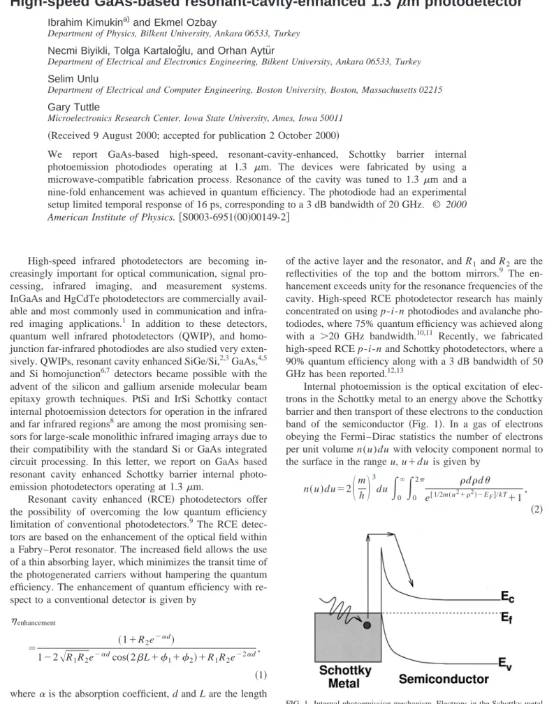
Internal photoemission is the optical excitation of elec-trons in the Schottky metal to an energy above the Schottky barrier and then transport of these electrons to the conduction band of the semiconductor 共Fig. 1兲. In a gas of electrons obeying the Fermi–Dirac statistics the number of electrons per unit volume n(u)du with velocity component normal to the surface in the range u, u⫹du is given by
n共u兲du⫽2
冉
m h冊
3 du冕
0 ⬁冕
0 2 dd e关1/2m共u2⫹2兲⫺EF兴/kT⫹1 , 共2兲a兲Electronic mail: [email protected]
FIG. 1. Internal photoemission mechanism. Electrons in the Schottky metal are excited to an energy above the Schottky barrier and then they transport to the conduction band of the semiconductor.
APPLIED PHYSICS LETTERS VOLUME 77, NUMBER 24 11 DECEMBER 2000
3890
0003-6951/2000/77(24)/3890/3/$17.00 © 2000 American Institute of Physics
where EF is the Fermi energy level, m is the electron mass, and T is the temperature. After evaluation of the integral, Eq.
共2兲 can be expressed as n共u兲du⫽4kT m
冉
m h冊
3log关e共EF⫺1/2mu2兲/kT⫹1兴du. 共3兲
According to the theory developed by Fowler, the number of electrons emitted per quantum of light absorbed is to a first approximation proportional to the number of electrons per unit volume of the metal whose kinetic energy normal to the surface is sufficient to overcome the potential step of the surface.14,15 The number of electrons that can go over the Schottky barrier and contribute to the photocurrent is given by
N⫽
冕
1/2mu2⫽EF⫹B⫺h
⬁
n共u兲du. 共4兲
The internal quantum efficiency is proportional to the num-ber of excited electrons to the conduction band. For the pho-ton energies higher than the potential barrier, Eq. 共4兲 can be approximated to obtain an expression for the internal quan-tum efficiency as a function of the photon energy
⬀共h⫺B兲2, 共5兲
whereis the photon frequency, andBis the barrier height. We used the transfer matrix method to design the epil-ayer structure and to simulate the optical properties of the photodiode. The epilayer structure of the photodiode was grown by a solid-source molecular beam epitaxy on a semi-insulating GaAs substrate. The bottom mirror was made from quarter-wave stacks of GaAs and AlAs designed for high reflectance at 1300 nm center wavelength. On top of the bottom mirror, a 300-nm-thick undoped GaAs layer was grown for mesa isolation. This layer was followed by a 600-nm-thick GaAs layer doped at 1018cm⫺3for ohmic contact, and a lightly doped 200-nm-thick GaAs layer for the Schottky contact. Cavity layers were completely transparent at wavelengths longer than 900 nm, and the absorption at these wavelengths occurred at the Schottky metal only.
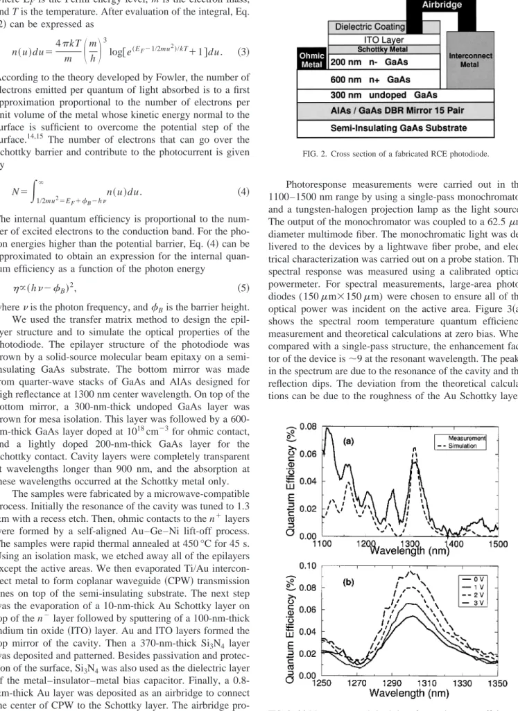
The samples were fabricated by a microwave-compatible process. Initially the resonance of the cavity was tuned to 1.3 m with a recess etch. Then, ohmic contacts to the n⫹layers were formed by a self-aligned Au–Ge–Ni lift-off process. The samples were rapid thermal annealed at 450 °C for 45 s. Using an isolation mask, we etched away all of the epilayers except the active areas. We then evaporated Ti/Au intercon-nect metal to form coplanar waveguide 共CPW兲 transmission lines on top of the semi-insulating substrate. The next step was the evaporation of a 10-nm-thick Au Schottky layer on top of the n⫺layer followed by sputtering of a 100-nm-thick indium tin oxide共ITO兲 layer. Au and ITO layers formed the top mirror of the cavity. Then a 370-nm-thick Si3N4 layer
was deposited and patterned. Besides passivation and protec-tion of the surface, Si3N4was also used as the dielectric layer
of the metal–insulator–metal bias capacitor. Finally, a 0.8-m-thick Au layer was deposited as an airbridge to connect the center of CPW to the Schottky layer. The airbridge pro-cess was essential to obtain high speed devices with very low parasitic capacitances. The cross section of a fabricated pho-todiode is shown in Fig. 2.
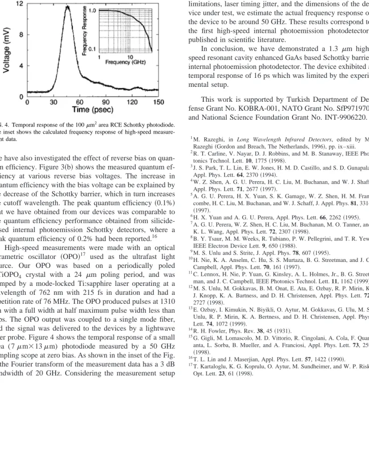
Photoresponse measurements were carried out in the 1100–1500 nm range by using a single-pass monochromator and a tungsten-halogen projection lamp as the light source. The output of the monochromator was coupled to a 62.5m diameter multimode fiber. The monochromatic light was de-livered to the devices by a lightwave fiber probe, and elec-trical characterization was carried out on a probe station. The spectral response was measured using a calibrated optical powermeter. For spectral measurements, large-area photo-diodes (150m⫻150m) were chosen to ensure all of the optical power was incident on the active area. Figure 3共a兲 shows the spectral room temperature quantum efficiency measurement and theoretical calculations at zero bias. When compared with a single-pass structure, the enhancement fac-tor of the device is⬃9 at the resonant wavelength. The peaks in the spectrum are due to the resonance of the cavity and the reflection dips. The deviation from the theoretical calcula-tions can be due to the roughness of the Au Schottky layer.
FIG. 2. Cross section of a fabricated RCE photodiode.
FIG. 3. 共a兲 Measurement and simulation of spectral quantum efficiency at room temperature.共b兲 Room temperature measurement of spectral quantum efficiency at various reverse biases. The peak quantum efficiency at the resonance wavelength increases with bias.
3891
Appl. Phys. Lett., Vol. 77, No. 24, 11 December 2000 Kimukinet al.
We have also investigated the effect of reverse bias on quan-tum efficiency. Figure 3共b兲 shows the measured quantum ef-ficiency at various reverse bias voltages. The increase in quantum efficiency with the bias voltage can be explained by the decrease of the Schottky barrier, which in turn increases the cutoff wavelength. The peak quantum efficiency共0.1%兲 that we have obtained from our devices was comparable to the quantum efficiency performance obtained from silicide-based internal photoemission Schottky detectors, where a peak quantum efficiency of 0.2% had been reported.16
High-speed measurements were made with an optical parametric oscillator 共OPO兲17 used as the ultrafast light source. Our OPO was based on a periodically poled KTiOPO4 crystal with a 24 m poling period, and was pumped by a mode-locked Ti:sapphire laser operating at a wavelength of 762 nm with 215 fs in duration and had a repetition rate of 76 MHz. The OPO produced pulses at 1310 nm with a full width at half maximum pulse width less than 1 ps. The OPO output was coupled to a single mode fiber, and the signal was delivered to the devices by a lightwave fiber probe. Figure 4 shows the temporal response of a small area (7m⫻13m) photodiode measured by a 50 GHz sampling scope at zero bias. As shown in the inset of the Fig. 4, the Fourier transform of the measurement data has a 3 dB bandwidth of 20 GHz. Considering the measurement setup
limitations, laser timing jitter, and the dimensions of the de-vice under test, we estimate the actual frequency response of the device to be around 50 GHz. These results correspond to the first high-speed internal photoemission photodetectors published in scientific literature.
In conclusion, we have demonstrated a 1.3 m high-speed resonant cavity enhanced GaAs based Schottky barrier internal photoemission photodetector. The device exhibited a temporal response of 16 ps which was limited by the experi-mental setup.
This work is supported by Turkish Department of De-fense Grant No. KOBRA-001, NATO Grant No. SfP971970, and National Science Foundation Grant No. INT-9906220.
1
M. Razeghi, in Long Wavelength Infrared Detectors, edited by M. Razeghi共Gordon and Breach, The Netherlands, 1996兲, pp. ix–xiii.
2R. T. Carline, V. Nayar, D. J. Robbins, and M. B. Stanaway, IEEE
Pho-tonics Technol. Lett. 10, 1775共1998兲.
3
J. S. Park, T. L. Lin, E. W. Jones, H. M. D. Castillo, and S. D. Gunapala, Appl. Phys. Lett. 64, 2370共1994兲.
4W. Z. Shen, A. G. U. Perera, H. C. Liu, M. Buchanan, and W. J. Shaff,
Appl. Phys. Lett. 71, 2677共1997兲.
5
A. G. U. Perera, H. X. Yuan, S. K. Gamage, W. Z. Shen, H. M. Fran-combe, H. C. Liu, M. Buchanan, and W. J. Schaff, J. Appl. Phys. 81, 3316
共1997兲.
6H. X. Yuan and A. G. U. Perera, Appl. Phys. Lett. 66, 2262共1995兲. 7A. G. U. Perera, W. Z. Shen, H. C. Liu, M. Buchanan, M. O. Tanner, and
K. L. Wang, Appl. Phys. Lett. 72, 2307共1998兲.
8B. Y. Tsaur, M. M. Weeks, R. Tubiano, P. W. Pellegrini, and T. R. Yew,
IEEE Electron Device Lett. 9, 650共1988兲.
9M. S. Unlu and S. Strite, J. Appl. Phys. 78, 607共1995兲. 10
H. Nie, K. A. Anselm, C. Hu, S. S. Murtaza, B. G. Streetman, and J. C. Campbell, Appl. Phys. Lett. 70, 161共1997兲.
11C. Lennox, H. Nie, P. Yuan, G. Kinsley, A. L. Holmes, Jr., B. G.
Street-man, and J. C. Campbell, IEEE Photonics Technol. Lett. 11, 1162共1999兲.
12M. S. Unlu, M. Gokkavas, B. M. Onat, E. Ata, E. Ozbay, R. P. Mirin, K.
J. Knopp, K. A. Bartness, and D. H. Christensen, Appl. Phys. Lett. 72, 2727共1998兲.
13E. Ozbay, I. Kimukin, N. Biyikli, O. Aytur, M. Gokkavas, G. Ulu, M. S.
Unlu, R. P. Mirin, K. A. Bertness, and D. H. Christensen, Appl. Phys. Lett. 74, 1072共1999兲.
14
R. H. Fowler, Phys. Rev. 38, 45共1931兲.
15G. Gigli, M. Lomascolo, M. D. Vittorio, R. Cingolani, A. Cola, F.
Quar-anta, L. Sorba, B. Mueller, and A. Franciosi, Appl. Phys. Lett. 73, 259
共1998兲. 16
T. L. Lin and J. Maserjian, Appl. Phys. Lett. 57, 1422共1990兲.
17
T. Kartaloglu, K. G. Koprulu, O. Aytur, M. Sundheimer, and W. P. Risk, Opt. Lett. 23, 61共1998兲.
FIG. 4. Temporal response of the 100m2area RCE Schottky photodiode. The inset shows the calculated frequency response of high-speed measure-ment data.
3892 Appl. Phys. Lett., Vol. 77, No. 24, 11 December 2000 Kimukinet al.