C.Ü. Fen Fakültesi
Fen Bilimleri Dergisi, Cilt 33, No. 1 (2012)
Calculation of Cutting Lines of Single-Walled Carbon Nanotubes
Erdem UZUN1*
1 Karamanoğlu Mehmetbey Üniversitesi, Fen Fakültesi, Fizik Bölümü, Karaman Received: 21.05.2012, Accepted: 19.06.2012
_____________________________________________________________________________________ Abstract. Carbon nanotubes (CNs) are hexagonally shaped arrangements of carbon atoms that have been rolled into
tubes with outstanding properties. Carbon nanotubes are among the stiffest and strongest fibers known, and have remarkable electronic properties and many other unique characteristics. All properties of the carbon nanotubes are determined by its electronic structure. The main focus of this study has been to investigate the basic electronic band structure of carbon nanotubes and to understand the origin of the cutting lines. For this purposes brief introduction to the electronic properties of carbon nanotubes was given and then 3D electronic band structure was plotted. For different chirality vectors (n, m) 1D and 2D first Brillouin zones and cutting lines of SWNT were calculated and plotted.
Key words: Single-walled carbon nanotube, Brillouin zone, Cutting line.
______________________________________________________________________________________________
1. INTRODUCTION
Following the discovery of carbon nanotubes (CTNs) in 1991 [1], the interest in carbon nanotubes increased rapidly because of their excellent mechanical and electrical properties and potential technological applications [2, 3, 4, 5, 6 and 7]. To obtain a typical carbon nanotube the graphene layer is bent in such a way that both ends of the vector lie on top of each other. The molecular structure is thus continuous around the tube [8, 9, 10 and 11].
2. THEORETICAL BACKGROUND
Graphene is a carbon allotrope whose structure consists of a stacking of two-dimensional, sp2-bonded carbon layers. CTNs are composed only of carbon atoms (C60)
arranged in a three-dimensional cylindrical shape and cage structure. __________________
* Corresponding author. Email address: [email protected]
In general, carbon nanotubes are divided into two categories; single-walled carbon nanotubes (SWNT) and multi-walled carbon nanotubes (MWNT). SWNT consisting only of one graphene sheet and MWNT with typically more than one rolled up sheets [2, 4, 5 and 6]. The geometry of SWNT can be imagined as one layer of graphite rolled in a seamless cylinder with a typical diameter of 1−2 nm. The lengths of the two types of tubes can be up to hundreds of microns or even centimeters. Band structure of SWNT will perform simple tight-binding model for a two dimensional (2D) sheet of graphene [11, 12 and 13].
The unit cell of the graphene sheet contains two carbon atoms and each of them has four valence electrons (see in figure 1), where three of them make sp2 bonds forming σ-orbits and fourth electron resides in a π-orbit extending perpendicular to the graphene plane. Since the π– bonds are much weaker than the σ–bonds the electronic properties of carbon nanotubes can be described taking into account only the π–electrons [4, 5, 6, 14 and 15]. Using the tight binding approximation [5, 6, 15 and 16], energy dispersion of the π–electrons of a graphene sheet is given by equation 1 and 2 [2, 4, 5, 6 and 7]. The energy structure of crystals depends on the interactions between orbits in the lattice. The tight binding approximation neglects interactions between atoms separated by large distances, an approximation which greatly simplifies the analysis and calculates the electronic band structure using an approximate set of wave-functions based upon superposition of orbits located at each individual atomic site [16]. The band structure of graphene is obtained from the tight binding approximation including only first-nearest-neighbor carbon-carbon interactions of –orbits of a single honeycomb graphite sheet. This is given by a simple analytical relation, derived by diagonalization of the 2×2 Bloch Hamiltonian for the diatomic graphene unit cell [1, 3, 15, 17, 18 and 19].
(1)
(2)
(3)
where o = 2.5 eV is the energy overlap integral (tight binding hopping parameter) between the nearest neighbors, is the on-site energy parameter, s is the overlap parameter, a is lattice parameter of graphene, the v and c indices stand for valence and conduction bands, respectively, and k = (kx, ky) represents the 2D wave-vector components along the x and y directions in the
2D Brillouin zone (BZ) of graphene. The parameters o and are expressed in electron-volt units (eV), whereas s is given in non-dimensional units. Conduction and valence bands are the
consequence of two carbon atoms per unit cell. The conduction band and the valence band meet at six distinct points corresponding to the corners of the first BZ. These points are referred to as K-points. Three out of the six K-points are equivalent due to the spatial symmetry of the hexagonal lattice, thus two distinguishable points remain called K and K’. At the special points K and K' of the graphene BZs the valence and conduction bands cross at the Fermi level (energy at 0 eV). Because of the same number of states in the first BZ as in real space and two carbon atoms per unit cell, at T =0K only the valence states are occupied, with a Fermi energy lying exactly at the position where the two bands cross [4, 5, 6, 14 and 15].
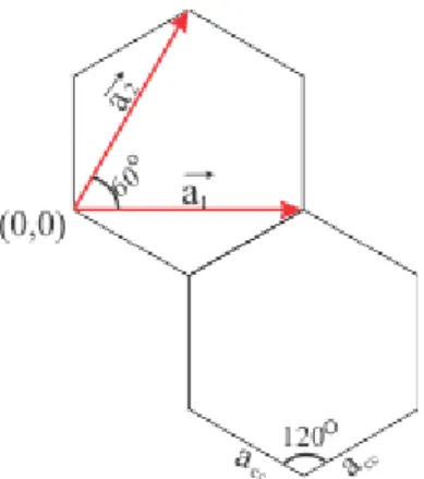
In figure 1 is illustrated a hexagonal lattice of a graphene sheet and corresponding lattice vectors (a1, a2) in real space. The lattice vectors make of an angle 60° [1, 2, 4, 5, 6 and
15].
Figure 1. Graphene lattice and lattice vectors
In real space lattice vectors are determined by Eq. 4a and b [2, 4, 5, 6, 7 and 20].
(4a)
(4b)
Where and is unitary basis vectors. Unit cell is arbitrary due to random selection of the coordinate system [20].
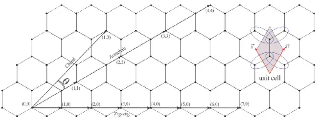
A specific carbon nanotube is defined by a chiral vector (eq. 5) which is shown in figure 2 with the unit vectors of the hexagonal lattice and n, m are integers ( ). Axis with special symmetries are the zigzag (n, 0), armchair (n, n) and chiral (n, m) directions named according to the line-shape of a tube circumference following the carbon atoms. They
are shown in figure 2. A SWNT is formed by joining the parallel lines which are defined by the starting and ending point of the chiral vector [2, 4, 5, 6, 7, 13, 17, 20 and 21].
Figure 2. Sketch of a graphene sheet, special symmetries and unit cell
(5)
Single-walled carbon nanotube diameter r and chiral angle ;
(6)
(7)
θ represents the angle between the chiral vector and the direction (n; n).
The reciprocal vectors are given in eq. 8 and 9 and they are related to the real lattice vectors according to the equation 10 [7, 8 and 21].
(8) (9) (10)
Where is the Kronecker function.
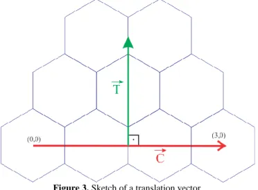
The fundamental property of an infinitely long SWNT is its translational periodicity and it is described by translation vector . The translation vector defines the length of the nanotube
unit cell and it is shown in fig.3. In a plain graphene sheet, vector along the axial direction of the SWNT and is the orthogonal to the chiral vector [17 and 21].
(11)
(12)
Where dc is the greatest common devisor (gcd) of (2n+m) and (2m+n).
Figure 3. Sketch of a translation vector
The chiral vector and translation vector define the translational unit cell of the SWNT. The number of unit cells of the translation unit cell is given by eq. 13.
(13)
The reciprocal lattice vectors and for a carbon nanotube are defined by eq.14a and b.
(14a)
(14b)
The and vectors define the seperation between the adjanted cutting lines and the length of cutting lines, respectively. In terms of the vectors and , the quantization condition expressed by eq.15 [15 and 21].
(15)
If there are N hexagons in the translational unit cell of the SWNT, the first Brillouin zone of the SWNT consists of N cutting lines. These cutting lines must be arranged into a rectangle with the sides parallel to the and vectors. Only then can the first BZ be folded into one dimensional reciprocal space of the SWNT. These BZs have rectangular shapes of different dimensions [9 and 21].
The reciprocal lattice of SWNT is obtained by folding reciprocal lattice of the graphene sheet. This is known as zone-folding approximation. The zone-folding approximation is that the electronic band structure of a nanotube is given by the superposition of the graphene electronic energy bands along the corresponding allowed k lines. The standing waves are characterized by their angular momentum (µ). The angular momentum of a standing wave in the SWNT corresponds to the linear momentum k of a plane wave of graphene sheet such that:
=2.µ (16)
The allowed wave-vectors in the reciprocal space of graphene is
(17)
Where k is the linear momentum along the SWNT axis [10, 19 and 21].
If we use eq. 17 for ky, discreteness of the ky values, leads to a one dimensional (1D) dispersion
relation in the eq 18.
(18)
For discrete values of µ, the above expression generates a set of equidistant parallel lines. These lines are known as cutting lines [21]. If we assumed that there are N hexagons in the translational unit cells of SWNT, we conclude that the fist BZ of the SWNT consist of N cutting lines. The cutting lines must be arranged into a rectangle with a side parallel to the reciprocal lattice vectors. The dimensions of the rectangular BZ are determined by the choice of the reduced unit cell [21].
The graphene sheet is a zero-gap semiconductor with the Fermi surface reduced to two points, and . The electrons at the Fermi surface are thus scattered either within the same or point by the phonon modes around the Γ point, or between different and points by the phonon modes near the or point [4 and 15]. The allowed wave vectors are on the so called cutting lines [21].
The cutting lines are that the one-dimensional (1D) BZ plotted on the extended two-dimensional (2D) BZ of graphene. The conduction and the valence bands meet at six distinct points (K-points) corresponding to the corners of the first BZ [15, 21 and 22]. Three of them are equivalent due to the spatial symmetry of the hexagonal lattice, thus two distinguishable points remain called K and K’ [21].
There are N cutting lines for (n,m) SWNTs. The ordinal number µ of the cutting lines starting from the Γ point µ =0 [21]. The k points on the µth cutting line of the (n,m) SWNT in the 2D BZ of graphite is given by eq. 19 [21].
(19)
3. SIMULATIONS and RESULTS
In this study, all simulations and calculations were carried out in wolfram Mathematica. Graphene is a single layer of carbon atoms densely packed in a honeycomb lattice. The energy structure of crystals depends on the interactions between orbits in the lattice. The tight binding approximation neglects interactions between atoms separated by large distances an approximation that greatly simplifies the analysis. Thus, the electronic band structure of graphene can be calculated by using the tight binding approximation. In this study, the band structure of graphene is obtained from the tight binding approximation including only first-nearest-neighbor carbon-carbon interactions of -orbits of a single honeycomb graphite sheet and then, the band structure of graphene was plotted by solving eq.1, 2 and 3 for 2D and 3D honeycomb crystal lattice of graphene under the tight binding approximation.
In this study, all simulations and calculations were carried out by using a computer code given in Mathematica. Figure 4 shows 3D electronic band structure of SWNT, where the bands cross the Fermi level (energy E=0 eV) for the electron energy dispersion for and *-bands in the first BZ at equidistant energies as pseudo-3D representations for the 2D structures. In this
figure, the valence band and the conduction band touch each other at K-points on the corner of the first BZ. Figure 5 shows the 2D tight-binding electronic band structure of a SWNT of any chirality (n, m) vector according to the zone-folding method. High symmetry points, , K and K' of the first Brillouin zone are also plotted.
Figure 4. 3D electronic band structure of SWNT
For different chirality vectors, the one dimensional dispersion relation (eq. 18) was used and the band structure of nanotube was plotted in figure 6. One can be seen from figure 6 that when the ky values are aligned with the special corner points K of the Brillouin zone, the SWNT
behaves as a metal. For armchair SWNT (n, n) there are in total 2n dispersion relations in the valence and 2n in the conduction band. Each band is doubly degenerate, except for the ones crossing E = 0 and the ones with maximal and minimum energy. Only, the ky =0 (µ = n) band
and the two outermost bands are non degenerate. However, for different chiral vectors the boundary conditions on around the circumference of a SWNT are not as simple as in the case of armchair or zig-zag SWNT. This situation can be visualized by the rotated orientation of quantized ky values in reciprocal space (Fig 6a, c and f. See also fig 7a, c and f). In specific
cases it is possible that none of the allowed ky values cross the K points, which results in an
energy gap, i.e. semiconducting properties (Fig 6b, d, e).
In the directions of the nanotube axis the wavevector kx is bounded to first Brillouin
zone, -/a kx /a. Although the graphene sheet can be rolled-up in an infinite number of ways,
three different classes of energy dispersion emerge near the Fermi level, as shown in fig 6 (i- 6a, c, f; ii- 6b, e; iii- 6d). In fig. 6a, c and f no states are available near the Fermi energy; these nonotubes are semiconducting. The two other energy dispersion (6b and e) have states at the Fermi energy; these nonotubes are metallic. In fig. 6d that nanotubes are in fact metallic tubes, but due to perturbation the lowest conduction band and the highest valence band do not touch each other in at K-points.
(c) (d)
(e) (f) Figure 6. 1D electronic band structure of a SWNT
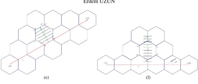
For different chirality vectors cutting lines of SWNT were calculated and plotted in figure 7. Figure 7 shows the construction of the first Brillouin zone of a SWNT superimposed on the 2D hexagonal first Brillouin zone of graphene. The first BZ of a SWNT is given by cutting-lines whose spacing and length are related to the chiral indices (n, m) of the nanotube. These are diameter, chiral angle, length of the unit cell along the tube axis, number of graphene unit cells inside the SWNT unit cell. All the points on the cutting lines belong to the SWNT BZ, thus it is a subset of points belonging to the graphene BZ. The SWNT electronic band structures are given by eq. 19, where K1 and K2 are the basis wave-vectors in the SWNT BZ. The spacing
between cutting lines is inversely proportional to the SWNT diameter (∆k= r / 2, see fig 7a), while the length of the lines is inversely proportional to the length of the SWNT unit cell along the tube axis (equals 2π/ , see fig 7a). The irreducible number of bands is equal to the irreducible number of cutting lines, which is given by the number N of graphene unit cells inside the SWNT unit cell. From the characteristic features of the band plots for any given (n, m) chirality one can verify the close relationship existing between geometry and electronic structure in SWNTs. The different chirality of zigzag and chiral nanotubes means that the allowed k-lines for these nanotubes are rotated (by /6 degrees for zigzag nanotubes) and
orientated differently around the K points. Zigzag and chiral tubes will be metallic if the allowed k-lines do cross the K points and semiconducting otherwise.
(a) (b)
(e) (f)
Figure 7. Cutting lines of SWNT were calculated by using different chiral vectors.
4.
CONCLUSIONS
A SWNT is usually characterized by its chiral vector C which is defined by two integers (n;m) as well as two base vectors (Fig. 1 and 2). These two integers (n;m) determine the tube diameter r, the chiral angle of the tube, the chirality and the physical properties of a SWNT (Eq. 6 and 7). C also defines the two points in the graphite sheet that are joined together when we roll the sheet into a carbon nanotube. There are two special types of SWNTs: armchair-tubes (n,n) and zig-zag-tubes (n,0). All other tubes are called chiral-tubes (Fig 2). The translation vector, T, define the length of the nanotube unit cell (Fig. 3).
To understand the electronic properties of SWNTs, a simple way is to start with the band structure of graphene, which underlies also the band structure of the nanotubes. We performed a calculation of the SWNT band structure starting from a simple tight-binding model for a two dimensional sheet of graphene. Using the tight binding approximation and dispersion relation for a 2D graphene sheet (Eq. 1, 2 and 3) band structure of graphene were plotted. Band structure simulations show that the 3D valence and conduction band of graphene meet at six points corresponding to the corners of the first Brillouin zone shown in Fig. 4. Due to spatial symmetry, two sets of these points, K and K’, are inequivalent and they coincide with the corners of the first Brillouin zone (Fig. 5).
The electronic properties of a SWNT vary in a periodic way from metallic to semiconducting and are calculated by imposing periodic boundary conditions on the wave function along its circumference. The one dimensional dispersion relation (Eq. 18) for the -electrons of the graphene is plotted in Fig. 6 for different chirality vectors (n, m). For different chiral vectors the boundary conditions of a SWNT are not as simple as in the case of armchair
or zig-zag SWNT. This situation can be visualized by the rotated orientation of quantized ky
values in reciprocal space (Fig 7a, c, d and f). In specific cases it is possible that none of the allowed ky values cross the K points, which results in an energy gap (Fig 6a, c and f). For
discrete values of µ, the one dimensional dispersion relation expression (Eq. 18) generates a set of equidistant parallel lines. These lines are known as cutting lines. The dispersion relation can now be found by slicing the dispersion relation for graphene along the lines with allowed wave vectors. If one of these slices happens to cut through the K point the nanotube will be metallic and if the slice does not cut through a K point it will be semiconducting. Zigzag and chiral tubes will be metallic if the allowed k-lines do cross the K points and semiconducting otherwise. The size of the energy gap of semiconducting nanotubes and the subband spacing of both semiconducting and metallic nanotubes is inversely proportional to the diameter. The interline spacing cutting lines depends only on the diameter as r/2. Since the distance between the center and edge of a hexagon in reciprocal space equals , see in Fig. 7a.
REFERENCES
[1] Langer, L., Bayot, V., Grivei, E. and Issi, J-P., 1996. Quantum Transport in a Multiwalled Carbon Nanotube, Phys. Rev. Lett. 76, 479.
[2] Dresselhaus, M. S., Dresselhaus, G. and Eklund, P. C., 1996. Science of Fullerenes and Carbon Nanotubes, Academic Press, New York, NY.
[3] Dresselhaus, M. S., 2004. Nanotubes: A step in synthesis, Nature Materials 3, 665 - 666. [4] Mintmire, J., Dunlap, B., and White, C., (1992), Are Fullerene Tubules Metallic?, Phys.
Rev. Lett. 68, 631.
[5] Saito, R., Fujita, M., Dresselhaus, G. and Dresselhaus, M., 1992a. Electronic structure of chiral graphene tubules, Appl. Phys. Lett., 60, 2204.
[6] Saito, R., Fujita, M., Dresselhaus, G. and Dresselhaus, M. S., 1992b. Electronic structure of graphene tubules based on C60, Phys. Rev. B 46, 1804–1811.
[7] Endo, M., Iijima, S. and Dresselhaus, M., 1996. Carbon Nanotubes, Elsiver.
[8] Gräber, M. R., 2006. Accessing the quantum world through electronic transport in carbon nanotubes, Philosophisch-Naturwissenschaftlichen Fakultät der Universität Basel, Switzerland, 115.
[9] Ifadir, S., 2005. Liquid Effect On Single Contacted Carbon Nanotubes Grown By Chemical Vapor Deposition, Philosophisch-Naturwissenschaftlichen Fakultät der Universität Basel, Switzerland, 58.
[10] Buchs, G., 2008. Local Modification and Characterization of the Electronic Structure of Carbon Nanotubes, Philosophisch-Naturwissenschaftlichen Fakultät der Universität Basel, Switzerland, 184.
[11] Babić, B., 2004. Electrical Characterization of Carbon Nanotubes grown by the Chemical Vapor Deposition Method, Philosophisch-Naturwissenschaftlichen Fakultät der Universität Base, 1l8.
[12] Samsonidze, G. G., Barros, E. B., Saito, R., Jiang, J., Dresselhaus G. and Dresselhaus, M. S., 2007. Electron-phonon coupling mechanism in two-dimensional graphite and single-wall carbon nanotubes, Physical Review B, 75, 155420.
[13] Zheng, L. X., O'Connell, M. J., Doorn, S. K., Liao, X. Z., Zhao, Y. H., Akhadov, E. A., Hoffbauer, M. A., Roop, B. J., Jia, Q. X., Dye, R. C., Peterson, D. E., Huang, S. M., Liu, J. and Zhu, Y. T., 2004. Ultralong single-wall carbon nanotubes, Nature Materials 3, 673 -
676.
[14] Hamada, N., Sawada S. and Oshiyama, A., 1992. New one-dimensional conductors: Graphitic microtubules, Phys.Rev.Lett,. 68,1579.
[15] Saito, R., Dresselhaus G. and Dresselhaus, M. S., 1998. Physical Properties of Carbon Nanotubes, Imperial College Press.
[16] Kittel, C., Solid State Physics, 1996. Hoboken, NJ: John Wiley and Sons, Inc.
[17] Wildoer, J. W.G., Venema, L. C., Rinzler, A. G., Smalley, R. E. and Dekker, C., 1998. Electronic structure of atomically resolved carbon nanotubes, Nature 391, 59
[18] http://www.wolfram.com/
[19] Odom, T. W., Huang, J - L., Kim, P., Lieber, C. M., 1997. Atomic structure and electronic properties of single-walled carbon nanotubes, Nature 391, 62-64.
[20] O'Connell, M. J., Eibergen, E. D. and Doorn, S.K., 2005. Chiral selectivity in the charge-transfer bleaching of single-walled carbon-nanotube spectra, Nature Materials 4, 412 - 418 [21] Saito, R., Sato, K., Oyama, Y., Jiang, J., Samsonidze, G. G., Dresselhaus, G. and
Dresselhaus, M. S., 2005. Cutting lines near the Fermi energy of single-wall carbon nanotubes, Physical Review B 72, 153413.
[22] Samsonidze, G., Saito, R., Jorio, A., Pimenta, M. A., Souza Filho, A. G., Grüneis, A., Dresselhaus, G. and Dresselhaus, M. S., 2004. The Concept of Cutting Lines in Carbon Nanotube, Applied Physics A: Materials Science & Processing, Volume 78, Number 8,