7-8 September 2014
Institute of Physics, Azerbaijan National Academy of Sciences
Baku, Azerbaijan
www.iotpe.com
[email protected] [email protected]
ICTPE-2014 Number 1 Code 01POW07 Pages 1-6
An Improved Dual Boost Converter with Zero Voltage Transition
H. Donuk
1I. Iskender
2N. Genc
31. Electrical Engineering Department, Sirnak University of Sirnak, Sirnak, Turkey, [email protected]
2. Electrical Electronics Engineering Department, Gazi University, Ankara, Turkey, [email protected]
3. Electrical Electronics Engineering Department, Yüzüncüyıl University, Van, Turkey, [email protected]
Abstract- This work proposes a soft switching approach
for dual-boost converter using an auxiliary resonant circuit. The topology is composed of a general dual-boost converter and an auxiliary resonant circuit including one switch, inductor, capacitor and diode. The auxiliary resonant circuit helps the main switch to operate under ZVT and ZCS conditions. The auxiliary switch also operates at soft switching mode. Furthermore, the proposed circuit removes the voltage stress on the main and auxiliary switches. Under soft switching conditions the efficiency of the converter increases. The converter has various advantages compared with the conventional boost converters as higher boost rate with low duty cycle, lower voltage stress on components and higher efficiency.
Keywords: Zero Voltage Transition, Dual-Boost Converter, Boost Converter.
I. INTRODUCTION
DC-DC converters controlled by Pulse Width Modulation technique have a wide range of application areas. Operating the converter at high frequency decreases the converter volume and increases the power density of converter. However, increasing the operating frequency increases the switching losses and the Electromagnetic Interference (EMI) resulting reduction in efficiency of converter [1]. Basically, switching losses are composed of switching losses of switches due to overlapping of voltage and current, loss of diodes due to reverse recovery phenomenon and discharge loss of the parasitic capacitor [2].
To reduce the switching losses several suppressing cells are made as RC/RCD, polar/non-polar, resonance/non-resonant and active/passive cells. The switching losses are greatly reduced by zero voltage switching method (ZVS) and the zero current switching (ZCS) method.
There have been published many papers about boost converter with active soft-switching methods. Boost type converter switching at zero voltage (ZVT) is one of the soft switching techniques given in [3].
There are methods given in [3], [4] and [5] in which the snubber cells cannot eliminate all the switching losses. In [5-7] there are used multiple inductors that increase the volume and decrease the power density of the converter.
Soft switching techniques used in [6] and [8] reduces the losses but cannot remove the voltage stress of main and auxiliary switches.
The turn on and turn off losses are reduced in [9], but due to several numbers of elements the volume of the converter increases.
In another study [10] there are used more than one switch that increases the cost of the converter [10].
In the study given in [11] the active snubber circuit provides zero voltage transition modes for the main switch. There is no voltage and current stress on the main diode.
This work proposes a soft switching dual-boost converter that is able to turn on both the active power switches at zero voltages to reduce their switching losses and evidently raise the conversion efficiency. In this study dual-boost converter circuit is operating under soft switching technique and the efficiency of the converter increases by reducing the switching losses. The problem of voltage stress is also eliminated. The operation principles of the converter and the conditions for realization of soft switching are analyzed in detail, simulation analysis performed using PSpice is given. The simulation results show that all the switches are operating at soft switching state and the efficiency of the converter is improved.
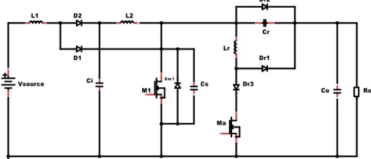
II. CIRCUIT CONFIGRATION
Figure 1 represents the circuit configuration of the proposed dual-boost pulse-width modulation (PWM) converter.
Figure 1. Proposed soft switched dual-boost DC/DC converter
Vsource L1 L2 Lr Ci Co Cr Cs Ro Ma D m 1 M1 D2 D1 Dr3 Dr1 Dr2 Ground
The converter consists of one switch; two boost inductors L1 and L2; two diodes D1 and D2; and capacitors
Ci and Co. Except the output capacitance of the converter,
the other components of the converter constitute the auxiliary circuit. Ma, Dr1, Dr2, and Dr3 represent the
auxiliary switch and diodes, respectively. The inductor and capacitor of proposed auxiliary circuit are presented by Lr and Cr, respectively. Dm1 is the intrinsic parallel
diode of MOSFET M1 and the snubber capacitance, Cs is
common for the main switch M1.
III. CIRCUIT OPERATION ANALYSIS
The following assumptions are made in analysis of the converter.
The output capacitor Co is large enough to
neglect reasonably the output voltage ripple and consider a constant level output voltage.
The forward voltage drops on MOSFET M1, Ma
and diodes D1 and D2 are neglected. Inductors L1 and L2 are large and equal. The components of the converter are ideal. The active switch, M1 is operated with
pulse-width-modulation (PWM) control signals. This is gated with identical frequency and duty ratio. The operation of the converter can be divided into seven modes, the equivalent circuits and the theoretical waveforms are illustrated in Figures 2 and 3.
A. Mode 1
Prior to this mode, the main switch M1 and the
auxiliary switch Ma are in the off state and output diode
Dr2 is conducting. At the beginning of this mode, Ma is
turned on. The resonant inductor (Lr) current starts to rise
through the path of Vsource-L1-L2-Lr-Ma. Since the rise rate
of this current is limited by Lr, the devices D1 and Ma are
turned on under soft switching. The voltage across Cs is
nearly equal to the output voltage (Vo) in this interval and
the initial voltage across the Cr is nearly equal to zero.
During this time interval, the voltage across Cr and
current of Lr can be expressed as: t0< t <t1
İLr (t) = Vcs Lr (t1- t0) = Vo Lr (t-t0) (1) VCr (t) =0 (2) (t1- t0) = ∆ t1 = İL1∗Lr Vo (3) Io (t) =IL1 - ICi - ILr (4) B. Mode 2
Ma current reaches iL1 and output current falls to zero
at t=t1 . The snuber capacitor (Cs) begins to discharge and
the current in Lr increases because of the resonance
between Lr and Cs. Cs is discharged until its voltage
reaches zero at t2. The resonant time period of this
interval, the current of Lr and voltage across Cs are given
by; t1 < t <t2 ILr (t) =i L1 + Vo Z1 * Sin ω1 (t –t1) (5) VCs (t) = Vo Cos ω1 (t –t1) (6) (t-t) = ∆t = π√LrCs (7) ω1 = 1/ √LrCs and Z = √LrCs C. Mode 3
At t=t2, the main switch and D2 are in the off state and
auxiliary switch and D1 are in the on state. Auxiliary
switch conducts the current in Lr. At the beginning of this
mode current of snubber capacitor Cs is completely
exhausted and the Lr current reaches its maximum rate.
At this interval, the current in Lr flows in Lr- Ma and
body diodes of the main switches. The voltage across Cr
is discharged nearly to zero before t2. The maximum
current of Lr can be equated as;
İLr (t) =ILrmax = IL1 +Vo / Z1 (8)
VCr (t) ≅ 0 (9)
At this mode, the main switch should be switched to satisfy the ZVT condition. By assuming the average inductor current of L1 is the half of the input current at
steady state, the delay time for M1, td can be expressed as;
td = ∆t1 + ∆t2 = Iin∗Lr
Vo +
π
2√LrCs (10)
Additionally, the current through inductors will start to increase linearly according to;
IL1 = Vs L1+Lr (t3-t2)≅ Vs L1 (t3-t2) (11) IL2 = VCi L2+Lr t ≅ VCi L2 t (12) D. Mode 4
At the start of this interval, Ma is turned off and the
main switch is turned on at the same time. At this mode, the main switche, M1 and Lr conduct the input current
together. At the end of this mode the current of Lr and
L1, L2 reaches zero. IL1 = Vs−Vo L1+Lr (t4-t3) ≅ Vs L1 (t4- t3) (13) IL2≅ Vci L2 (t6-t4) (14) E. Mode 5
This interval is composed of two equivalent circuit. The energy is stored in the boosting inductor L1 through
the loop of Vsource-L1-D1-M1 and stored in the boosting
inductor L2 through the loop of Ci-L2-M1. The energy is
transferred to the load through discharging capacitor, Co.
The current of L1;
IL1 = Vs
L1 (t5-t4) (15)
F. Mode 6
At t5, the current of main switch falls to zero and
voltage across of M1 and Cs go up to output voltage Vo.
At the end of this interval the current of Lr starts to
MODE 4 Ground Dr2 Dr1 Dr3 D1 D2 M1 D m 1 Ma Ro Cs Cr Co Ci Lr L2 L1 Vsource
Figure 2. Operational modes of proposed circuit converter.
G. Mode 7
At a certain moment t6, D2 and main switch are turned
off. D2, Dr1 and Dr2 are turned on. The inductor currents
IL1 and IL2 at the that moment have reached peak values.
The stored energy is supplied to load through diodes D2,
Dr1 and Dr2. As a result, the current through the inductors
IL1 andIL2 will start to decrease linearly according to;
IL1 = Vs−Vci L1 (t6-t7) (16) IL2 = Vci−Vo L2+Lr (t6-t7) (17)
Current Ci is inversed again, and Ci is now charging
until D1 is turned on again and the cycle with its seven
intervals is repeated.
IV. CİRCUIT DESIGN AND SELECTION OF COMPONENTS
The boost converter is a high-efficiency step-up DC/DC switching converter. The converter uses a switch to transfer power through pulse-width modulation technique. This section presents a design procedure for the proposed soft switched dual-boost converter operating in continuous conduction mode (CCM). In the periodic switching scheme with period T, the average voltage across the inductor must be zero. The relationship of voltage and current for an inductor is
VL = L diL dt, (18) İL (t) = 1 L∫ VL(t) dt t 0 +İL(0), (19) İL (t) = 1 L∫ VL(t) dt t t0 +İL(to), (20) İL (T+to) = 1 L∫ VL(t) dt T+t t0 +İL(to), (21) İL (T+to) - İL(to) = 1 L∫ VL(t) dt T+t t0 . (22) i(t)=i(t +T), t=to , and VL = 1 L∫ VL(t) dt T+t t0 =0
According to the voltage second product,
Vs *ton =(VCi - Vs)*toff or Vs T = VCi*toff (23)
VCi = T toff Vs = T T−ton Vs (24) VCi = 1 1−(Daux+Dmain) Vs, (25)
Deff =Daux +Dmain
Dmain is duty cycle of the main switch and Daux is the
duty cycleof the auxiliary switch. The same procedure is used to find the relation between the output voltage Vo
and the first stage output VCi:
VCi ton =(Vo – VCi) toff , (26)
VCi (ton+ toff) =Vo toff , (27)
Vo = T toff VCi = T T−ton VCi, (28) Vo ≅ 1 1−(Daux+Dmain) VCi ≅ 1 1−Deff VCi (29) Vo = 1 1−Deff VCi = 1 (1−Deff) 2. Vs (30)
The gain of the dual-boost DC-DC converter will be Vo ≅
1
(1−Deff) 2. Vs . (31)
To achive the zero voltage transition, a delay time (T ) of main switch PWM is required. The minimum
delay time must be satisfied the following equation. The time is consisted of the resonant time between Lr and Cs
and the time that the resonant inductor current equals the input current. Td ≥ Iin∗Lr Vo + π 2 √LrCs (32)
It is seen from equation (32) that Td depends on Vo,
Iin, Lr and Cs. During the delay time, the auxiliary switch
is turned on.
The input current ripple ∆IL on each of the boost
inductors can be denoted as: ∆IL ≅∆IL1 =
𝐷𝑒𝑓𝑓
𝐿1∗𝑓 Vs, (33)
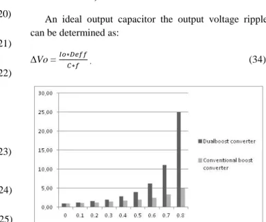
An ideal output capacitor the output voltage ripple can be determined as:
∆Vo= 𝐼𝑜∗𝐷𝑒𝑓𝑓
𝐶∗𝑓 , (34)
Figure 4. Voltage conversion ratio.
V. SIMULATION
In this section, simulations are carried out to verify the theoretical analysis given in the previous sections. Since the PSpice simulation program includes models of the real components, the proposed topology is firstly simulated via this program and the simulation results of the proposed topology are shown in the following figures. The converter design specifications are considered for medium power sources. Since the output voltage generated by the photovoltaic arrays and the fuel stack sources is relatively low, their output voltage is generally increased via conventional boost or dual-boost type dc-dc converters to the required voltage level. The converter specifications consist of,
Output power: Po =600 W,
Output voltage ripple, ∆Vo= %2, Input current ripple, ∆IL = %15,
Time 14.30ms 14.32ms 14.34ms 14.36ms I(L1) I(L2) 0A 10A -5A 15A Boost inductor (L2) Boost inductor (L1) Time 1.0200ms 1.0210ms 1.0220ms ID(Ma) VD(Ma)/10 0 40 -39
Auxiliary switch current Auxiliary switch voltage
Table 1. Components values for the simulation Components Symbols Parameters Input voltage Vsource 100 V
Output voltage Voutput 300 V Switching frequency f sw 50 kHz
Main inductances L1 and L2 300 uH
Auxiliary inductance Lr 1 uH Auxiliary capacitance Snubber capacitance Cr 5 nF Cs 1 nF Input capacitance Ci 30 uF Output capacitance Co 50 uF
Main switch M1 IRF250-30A
Auxiliary switch Ma IRF350-14A
Main diodes D1 and D2 MUR810
Auxiliary diodes Dr1 ,Dr2, Dr3 and Dm1 MUR810
Output power Po 600 W
Figure 5. Simulation waveforms of the current of the inductors (IL1 and
IL2)
Figure 6. Simulation waveforms of the voltage and current of the auxiliary switch Ma (VDMa/10, IDMa and Po= 600 W- Vo = 300 V)
Figure 7. Simulation waveforms of the voltage and current of the main switch M1 (VD/10, IDM1) under soft switching condition.( Po= 600 W- Vo
= 300 V )
Figure 8. Simulation waveforms of the voltage and current of the main switch M1 (VD/10, IDM1) under soft switching condition turn on. (Po=
600 W- Vo = 300 V )
Figure 9. Simulation waveforms of the voltage and current of the main switch M1 (VDM1, IDM1) under soft switching condition turn off (Po= 600
W- Vo = 300 V)
Figure 10. Simulation waveforms of the voltage and current of the main diode D1 (VD1 , ID1 *5) under soft switching condition (Po= 600 W- Vo
= 300 V)
Figure 11. Simulation waveforms of the voltage and current of the main diode D2 (VD2 , ID2 *5) under soft switching condition (Po= 600 W- Vo
= 300 V) Time 18.1400ms 18.1450ms 18.1500ms 18.1355ms ID(M1) VD(M1)/10 0 40 80 -35 VDM1 IDM1 Time 18.1450ms 18.1500ms 18.1550ms 18.1419ms ID(M1) VD(M1)/10 0 40 -30 VDM1 IDM1 ZCS Time 18.1380ms 18.1400ms 18.1420ms 18.1440ms 18.1466ms ID(M1) VD(M1)/10 0 40 -30 VDM1 IDM1 ZVT Time 44.74ms 44.76ms 44.78ms I(D1)*5 V(D2:1,D1:2)*-1 0 100 200 -92 ID1 VD1 Time 44.74ms 44.76ms 44.78ms I(D2)*5 V(D2:1,D2:2)/-1 0 100 200 -92 ID2 VD2
Figure 12. Simulation waveforms of the voltage and current of the auxiliary diode Dr2 (VDr2/15, IDr2) under soft switching condition (Po=
600 W- Vo = 300 V)
Figure 13. Simulation waveforms of the voltage and current of the auxiliary diode Dr3 (VDr3/20, IDr3 *5) under soft switching condition
(Po= 600 W- Vo = 300 V)
From the simulation results given in figures 12 and 13, it is seen that the main switch M1 is turned on
perfectly with ZVT and turned off under near ZCS. Figure 9 shows auxiliary switch, Ma which is turned on
and off under soft switching. Also, the devices D1, D2,
Dr1, Dr2 and Dr3 operate under soft switching conditions.
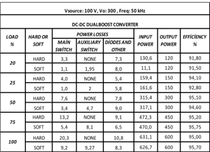
The losses of the semiconductor devices and the total efficiencies of the circuits for hard switching and the proposed soft switching cases are summarized for various loads as given in Table 2.
Table 2. Losses of the semiconductor devices and total efficiencies of
the circuits in the hard switching and the proposed soft switching converter
At 450 W output power in the hard switching operation the main switch loss is about 13,2 W and this loss is equal %59,1 of total loss of circuit. At 450 W output power in the proposed soft switching converter, the main
switch loss is about 5,4 W and this loss is equal %27 of total loss of circuit.
Figure 14. Overall efficiency curves of the hard switching and the proposed soft switching converters comparatively
VI. CONCLUSION
In this paper, a soft switching dual-boost converter using an auxiliary resonant circuit is proposed. Operation modes are divided considering the voltage and current waveforms. Equivalent circuit of each operation mode is illustrated and the current paths are indicated. Each mode is analyzed through the simulation. It is verified that the main switch operates at soft switching. The main switch is turned on with ZVT and turned off under near ZCS. The auxiliary switch turned on and turned off under the soft switching mode. In addition, the main diodes and auxiliary diodes turn on and off under soft switching cases. It can be clearly seen that the predicted operation principles and analysis of the proposed converter are verified with all of the simulation results. In the proposed converter, most of the drawbacks of the conventional ZVT converter are overcome both perfectly and easily. All the semiconductor devices of the converter are both turned on and off under soft switching state. There is no any additional voltage and current stresses on the main devices and the auxiliary devices.
NOMENCLATURES
∆IL : Input current ripple ∆Vo: Output voltage ripple
Z : Impedance of the auxiliary circuit Deff : Effective duty cycle rate
……….
REFERENCES
[1] Huang, W. ve Moschopoulos, G., (2006). “ A New Family of Zero-Voltage-Transition PWM Converters with Dual Active Auxiliary Circuits”, Power Electrons, IEEE Transactions on, 21: 370-379
[2] Aksoy, İ., (2007). Yeni Bir Yumuşak Anahtarlamalı DC-DC PWM Dönüştürücünün Tasarımı, Analizi ve Uygulaması, Doktora Tezi, YTÜ Fen Bilimleri Enstitüsü, İstanbul.
[3] G. Hua, C. Leu, Y. Jiang and F. Lee “ Novel Zero-Voltage-Transition PWM Converters”, IEEE Transaction on Power Electronics, 9(2): 213-219 (1994).
[4] H. Bodur, A. F. Bakan “A new ZVT-PWM DC-DC Converter” IEEE Transaction on Power Electronics, 17(1): 40-47 (2002).
[5] M. Phattanasak, “A ZVT Boost Converter using an Auxiliry Resonant Circuit” Power Electronics, Drives and
Time 19.1800ms 19.2000ms 19.2200ms 19.1618ms I(Dr2) V(Dr2:1,Dr2:2)/-15 0 20.0 -13.7 33.6 VDr2 IDr2 Time 19.16ms 19.17ms 19.18ms 19.19ms I(Dr2)*5 V(Dr3:1,Dr3:2)/-20 0 100 200 IDr3 VDr3 MAİN SWİTCH AUXILIARY SWİTCH DİODES AND OTHER HARD 3,3 NONE 7,3 130,6 120 91,80 SOFT 1,1 1,95 8,0 11,1 120 91,50 HARD 4,0 NONE 5,4 159,4 150 94,10 SOFT 1,0 2 5,8 161,6 150 92,80 HARD 7,6 NONE 7,8 315,4 300 95,10 SOFT 3,4 4,7 9,0 317,1 300 94,60 HARD 13,2 NONE 9,1 472,3 450 95,20 SOFT 5,4 8,1 6,5 470,0 450 95,75 HARD 20,3 NONE 10,8 631,1 600 95,00 SOFT 9,2 9,27 8,3 626,7 600 95,70 20 25 50 75 100
Vsource: 100 V, Vo: 300 , Freq: 50 kHz DC-DC DUALBOOST CONVERTER LOAD
%
HARD OR SOFT
POWER LOSSES INPUT
POWER OUTPUT
POWER
EFFİCİENCY %
Energy Systems, 2006. PEDES’06 International Conference on,pp.1-6,12-15 Dec. 2006
[6] A.F. , Bakan, H., Bodur, and I., Aksoy, “A Novel ZVT-ZCT-PWM DC-DC Converter”, 11th Europen Conference on Power Electronics and Applications (EPE2005), Dresden, pp.1-8,Sept.2005
[7] R. Gurunathan and A.K.Bhat ,”ZVT boost converter using a ZCS auxiliary circuit, ” IEEE Trans. Aerosp. Electron. Syst.,vol. 37, no.3 ,pp.889-897,Jul.2001 [8] Iskender, I., & Genc, N. (2010). “Design and analysis of a novel zero-voltage-transitions interleaved boost converter for renewable power applications.” International Journal of Electronics, 97, 1051-1070. doi: 10.1080/00207217.2010.482021
[9] Jain, N., Jain, P., and Joos, G.(2001) “ Analysis of a zero voltage transition boost converter using a soft switching auxiliary circuit with reduced condition losses ” in IEEE PESC Conference Record, Vol. 4,2001 , 1799-1804.
[10] Gurunathan, R. and Bhat, A. K. S.,” A zero-voltage-transition boost converter using a zero voltage switching auxiliary circuit”, IEEE Transactions on Power Electronics, 17:658-668 (2002).
[11] Bodur, H. and Bakan, A.F., (2004). “A New ZVT– ZCT–PWM DC–DC Converter”, IEEE Trans. On Power Electron, 19(3): 676-684.
[12] Khairy, S., Mazen, A., Adel, A., and Mahmoud, A.,”New High Voltage Gain Dual-boost DC-DC Converter for Photovoltaic Power Systems”, Electric Power Components and Systems, 40:711-728, 2012 ……….
BIOGRAPHIES
Hakan Donuk was born in Diyarbakir, Turkey, 1987. He received the B.Sc. degree in Electric and Electrical Engineering from Dicle University, Diyarbakir, Turkey and is currently working on his MS thesis in Gazi University. His research areas include soft switching, active-passive snubber cells in power electronics, renewable energy.
Ires Iskender received his M.Sc. and
Ph.D. degrees in Electrical and Electronic Engineering in 1990, 1996, respectively, from Middle East Technical University, Turkey. He is currently an Professor in the Department of Electrical and Electronic Engineering, Gazi University, Ankara, Turkey. His research interests include power electronic, renewable energy, fuzzy control, electrical machine, power quality
Naci Genc completed his B.S. in
Electrical Education Department from Gazi University, Ankara. He received his MS from Electrical & Electronics Engineering Department of Yuzuncu Yil University and Ph.D. Degrees from Electrical & Electronics Engineering
Department of Gazi University in 2002 and 2010, respectively. From 1999 to 2010 he worked as a research assistant in the Electrical and Electronics Engineering Department of Yuzuncu Yil University, Middle East Technical University and Gazi University, Turkey. He is currently an Associate Professor at Yuzuncu Yil University, Van. His research interests include power electronics, electrical machines, renewable energy, solar photovoltaic energy systems and control systems.