The effect of rotational angle on adsorption and electronic properties
Merve Yortanlı and Ersen Mete∗Department of Physics, Balıkesir University, Balıkesir 10145, Turkey (Dated: September 10, 2019)
Graphene adsorption on Au(111) surface was explored to identify their common surface structures by means of van der Waals corrected density functional theory calculations. The alignment of graphene in the form of certain rotational angles on the gold surface has an important role on the lattice matching which causes Moir´e patterns, and on the electronic properties of the resulting common cell structures. The dispersive weak interactions between carbon and gold layers lead to a downward shift of Fermi energy of the adsorption system with respect to the Dirac point of graphene showing a p-type doping character. Moreover, the shift was shown to depend on the rotational angle of graphene on Au(111).
I. INTRODUCTION
Graphene is a two dimensional material made up of carbon atoms in a hexagonal lattice arrangement. It receives a growing attention since its discovery in 2004 [1, 2], due to its unusual mechanical, thermal, elec-tronic and optical properties (e.g. impressive mechan-ical strength and flexibility, high thermal conductiv-ity, ultrahigh charge-carrier mobilconductiv-ity, and unique optical response).[3–5]
Theoretically, graphene can be modeled as a free-standing two dimensional sheet. In this form, graphene’s superior electronic conductivity is related to the conical singularities, at the corners of the hexagonal Brillouin zone, which show linear energy dispersion up to ±1 eV from the Fermi level. These structures also known as the Dirac cones where the upper and lower conicals from the conduction and valence bands touch at the Dirac point. This gives graphene a gapless electronic structure and massless charge-carriers which lead to novel topological phenomena such as quantum spin Hall effect.[6, 7]
The growth and transfer of free-standing graphene onto metal surfaces in control-based electronic device de-signs brings some difficulties about scalable production, desirable quality, and practicality. Moreover, design spe-cific functionality to graphene can be achieved either by dopants (such as boron nitride (BN) molecules, H, Al, Si, P and S atoms), or by adsorbing the graphene mono-layer onto a metal surface, or even by using graphene nanostructures like nanoribbons.[8–14]
The increasing demand for functional electronic appli-cations, such as display technologies, pushes researchers to develop substrate supported transparent conducting layers. Graphene monolayers with long-range order can be synthesized on metal surfaces via, for example, chem-ical vapor deposition (CVD).[15] Graphene coating on metal surfaces is an advantageous method which can be adapted to a wide range of areas such as electronics, solar
∗Corresponding author : [email protected]
cells, optoelectronics, sensor-technology and bio-devices. [16–23]
The growth of graphene monolayers on metal foils such as Cu leads to polycrystalline films with domains depend-ing on the crystallographic orientations. Moir´e super-structures were observed on epitaxial graphene which oc-cur due to matching of graphene lattice with that of the metal substrate depending on the periodic coincidence and the rotational angle between them.[12, 24] Wofford et al.[25] synthesized and observed graphene orientation in a R30 alignment on Au(111) using low-energy electr-ron diffraction (LEED). In this study, one of the aims is to identify a number of small size common surface cell structures of graphene and gold (111) by consider-ing possible rotational alignments. The choice of gold as the substrate has some advantages such as its low C sol-ubility, inert surfaces to oxidation, lower vapor pressures relative to that of Cu, and re-usability.[25]
The adsorption and electronic properties of graphene/metal surface structures must be well un-derstood for highly efficient device designs. For this reason there are many experimental studies to elaborate the mechanism of graphene adsorption on metal surfaces. [26–39] For instance, the interaction between graphene and Ti(0001), Ni, Pd and Co (111) surfaces are known to be stronger (chemisorption) relative to physisorption on Au, Ag, Pt, Al, Ru surfaces. The reasons leading to these two adsorption regimes, and their affects on the chemical and electronic properties of grapheme/metal systems have been investigated by many theoretical studies.[40–57] The Dirac conical structure of graphene is less affected at the weak interfacial interaction regime. However, due to the difference in graphene and metal surface work functions, Fermi level of the total system shifts up relative to the Dirac point on Ag, Al, Cu substrates (n-type doping) or down on Au, Pt substrates (p-type doping). The upward or downward shift of Fermi level is considered to be associated with the work functions of graphene and the corresponding transition metal surface.[46, 58] In addition, the equilibrium dis-tance between adsorbed graphene and the metal surface determines the Fermi level shift.[41] Chemisorption on
Ni, Pd and Co surfaces, on the other hand, is due to the strong interaction between the pz orbitals of C atoms
graphene and the d orbitals of the metal surface. In this case, the band structure of graphene changes and mixes with that of metal substrate.[40, 46]
The computational studies usually consider (2×2) su-percell of graphene as the smallest common structure for graphene and metal surfaces. There is a need to de-termine the possible common supercell structures with different periodicities. In this study, the metal substrate has been chosen as gold. Apart from the advantageous sides of gold as a substrate for the adsorption of graphene monolayers mentioned earlier, Au(111) is a well-known surface which is encountered in many applications such as self-assembled monolayers (SAM).[59–66] In recent years, there are a few studies on the application of graphene coating on gold surface-based SAMs.[67–69] For instance, Xie et al. comparatively analyzed the electrochemical properties of bare gold, of gold with n-octadecyl mer-captan (C18H37SH) SAMs, and of graphene adsorbed
SAM/Au system.[67] They reported that there was no electron transfer between the non-graphene/SAM struc-ture and the ruthenium hexamine redox probe, so the ma-terial exhibited insulating behavior. However, they ob-served an electron transfer between the graphene coated SAM and the redox probe. In another recent study, Yan et al. studied the photoemission characteristics of gold surface/diamondoid SAMs covered with graphene as the stabilizer/protector layer.[69] They reported that the graphene coating prevents the desorption of diamondoid molecules from the gold surface by forming a good bar-rier over the diamondoid SAMs. Such applications put forward the need to determine common surface super-cells of hetero-layered structures which involve Au and graphene. The combination of gold and graphene has a great potential in different types of novel designs.
We systematically investigated the matching periodic-ities of graphene on Au(111) to determine their several common surface cells using modern dispersion corrected DFT calculations. One of the main focuses has been given to elaboration of the adsorption geometries, in-terlayer binding characteristics, energy bands, and work functions of these structures. Since different common geometries are expected to show various atomic coin-cidences, it becomes important to explore the effect of such differences between the common periodicities on the adsorption and electronic properties of graphene on Au(111).
II. THEORETICAL METHOD
Total energy density functional theory (DFT) calcula-tions in the framework of the projected augmented wave method (PAW) have been performed using VASP [70– 73]. Single-particle orbitals were expanded in the plane wave basis up to a kinetic energy cut-off value of 400 eV. The exchange-correlation (XC) effects have been
in-cluded based on the modern and nonempirical SCAN[74] (strongly constrained and appropriately normed) semilo-cal meta-Generalized Gradient Approximation (meta-GGA) density functional.
To achieve more consistent results for weakly inter-acting layered structures, van der Waals (vdW) forces must be taken into consideration. As known from the previous studies, the interaction between Au surface and graphene layer is a weak physisorption interaction.[40, 75] Hence, we have used SCAN+rVV10 exchange-correlation functional which includes dispersive corrections through non-local correlation functional rVV10.[76] In fact, re-cent studies showed that the SCAN+rVV10 vdW density functional produces excellent results for interlayer bind-ing energies of layered materials as well as the adsorption energies of graphene on transition metal surfaces.[77] In order to give a better description of the effect of the vdW-DFT approach on the computationally estimated values of the weakly interacting graphene/gold system, the re-sults obtained by using PBE functional, which is based on the standard generalized gradient approximation (GGA), are also presented.
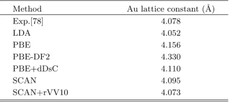
In addition, even though gold is a metallic system, use of different vdW functionals make a difference in the calculated lattice constant. As given in Table I, the SCAN+rVV10 functional yields the best estimation to the experimental value of 4.078 ˚A. [78] The in-plane lat-tice constant of graphene was found as 2.445 ˚A and 2.442 ˚
A with PBE and SCAN+rVV10 functionals in agreement with previous studies.[46]
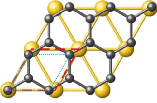
FIG. 1. Schematic representation of the graphene layer on the top layer of Au(111) surface. Dotted (blue) and dashed (red) lines indicate the unitcells of graphene and Au(111), repectively.
A four layer slab model was built to represent (111) surface of gold. Graphene is placed on gold surface such that their lattice translation vectors coincide as shown in Fig. 1. The magnitude of the in-plane translation vectors of gold and graphene were found by employing vdW cor-rections as 2.744 ˚A and 2.442 ˚A , respectively. Therefore, (1×1) unit cell of graphene has a 11% mismatch to that of gold. By rotating graphene monolayer on gold surface, matching supercell structures were explored. A strain of about %2 on graphene caused by adsorption on the gold surface is imposed as a criteria to identify common su-percells. The strain percentage on graphene is calculated
TABLE I. Comparison of the bulk Au lattice constant be-tween experimental and various XC functionals values.
Method Au lattice constant (˚A)
Exp.[78] 4.078 LDA 4.052 PBE 4.156 PBE-DF2 4.330 PBE+dDsC 4.110 SCAN 4.095 SCAN+rVV10 4.073 using, dfree C−C− dC−Cadsorbed dfree C−C × 100 where dfree C−C and d adsorbed
C−C are the C-C bond lengths in
free-standing and adsorbed graphene monolayers. Each of the computational cells consists of a four layer gold slab with a graphene adsorption monolayer obey-ing the same periodicity, and a 12˚A thick vacuum region to prevent any unphysical interaction between the pe-riodic images of the slabs. Methfessel-Paxton smearing with σ= 0.05 was used in the calculations. Atomic co-ordinates were optimized self-consistently until Hellman-Feynmann forces acting on each atom at each of the three cartesian directions became less than 10−2 eV/˚A. No atom was frozen to its bulk position. In the geometry optimizations, surface Brillouin zone (BZ) integrals were carried out by k-point samplings which were chosen prop-erly to be dense enough for a metallic system and to be compatible with the translational symmetry of the corre-sponding reciprocal cell. In the structure optimizations we switched off the symmetry operations which reduces the number of k-points in the irreducible BZ. For exam-ple, Γ-centered 6 × 6 × 1 k-point grid was used for the (4×4) computational cell which has a hexagonal symme-try. The naming of the common supercell structures is hereinafter adapted with respect to the (111) surface of gold. Similarly, an 8 × 8 × 1 k-point mesh was chosen for (3 × 3) and (√7 ×√7)R19.12◦ supercells. For the (√3 ×√3)R30◦ structure 10 × 10 × 1 k-point sampling was enough to get energy values converged to a few meVs. In the relaxation of the (7 × 7) superstructure, the BZ integrations were performed over a 4 × 4 × 1 k-point grid. In order to describe the physisorption of a graphene monolayer on Au(111) with different possible common periodicities, the average adsorption energy Eadsper
car-bon can be obtained using the following formula, Eads= (EG/Au(111)− EAu(111)− EG)/n
where EG/Au(111) is the total cell energy of graphene
ph-ysisorbed Au(111) slab. EAu(111)and EGare the energies
of clean gold surface model and the graphene monolayer,
respectively. In addition n in the denominator is the number of carbon atoms contained in the computational cell.
III. RESULTS AND DISCUSSION
A. Geometry and Adsorption
Common periodic structures of graphene/Au(111) were modeled by overlapping the lattice vectors of gold and graphene unit cells, and then rotating the graphene monolayer on the Au(111) surface. The in-plane lat-tice vectors and initial configuration of both structures are shown in Fig. 1. In this position, a common superstructure can be obtained which corresponds to graphene/Au(111)-(9 × 9)/(8 × 8) supercell. Due to its large size we did not include this geometry in this study. When the graphene monolayer is rotated 30◦ clockwise (or even counterclockwise) with respect to the in-plane lattice vectors of gold, it becomes commensurate with the (3 × 3) gold surface supercell (in Fig. 2c). We refer this geometry as (3 × 3)-GR30◦indicating that graphene has a rotational angle of 30◦ on Au(111) with a com-mon periodicity of (3 × 3) cell with respect to the gold surface. LEED experiments confirmed the existence of this R30 alignment structure.[25] At this rotational an-gle, other common superstructures of (3 ×√3)-GR30◦ and (√3 ×√3)R30◦-GR30◦ can be identified as given in Fig. 2a and Fig. 2b with slightly different mismatch val-ues. In particular, (√3 ×√3)R30◦-GR30◦ gold surface
cell (Fig. 2a) matches with (2 × 2) supercell of graphene. The strain ratios for these three geometries are all about −0.4% with the PBE and −2% with the SCAN+rVV10 functionals as shown in Table II where negative strain refers to shrinking.
Since the angle between the in-plane lattice vectors (or rows of gold atoms) of gold is 60◦ giving a hexagonal arrangement, rotation of graphene monolayer by an angle of 10◦ or 50◦ results in the same geometry. Therefore, graphene/Au(111) (4×4) superstructure shown in Fig 2d can either be called as (4 × 4)-GR10◦ or equivalently as (4 × 4)-GR50◦
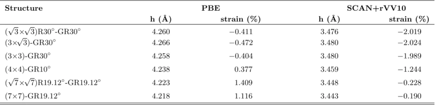
A larger, common geometry was identified at a rota-tional angle of 19.12◦ with a periodicity of (7 × 7) on the gold surface as depicted in Fig. 2f. At this rota-tional angle, another graphene/Au(111) superstructure can be identified with a slightly different mismatch value as (√7 ×√7)R19.12◦-GR19.12◦ (in Fig. 2e). Conse-quently, a total of six different common supercells were determined with low mismatch allowing probable Moir´e patterns.
Equilibrium distances and strain ratios of graphene monolayer on Au(111) surface were calculated using the PBE and the SCAN+rVV10 functionals, and pre-sented in Table II. The height of graphene monolayer from the topmost gold plane represents an average value over the separation distances of carbon atoms from the
FIG. 2. (a) DFT-optimized common surface structures of graphene on gold (111) using the SCAN+rVV10 XC functional. The periodic supercell geometries were indicated by red (solid) lines. The labeling of common superstructures follows that of Au(111) on the left, a dash in the middle, and the rotational angle of graphene on the right.
TABLE II. Minimum energy heights of graphene on Au(111) surface and the ratios of strain due to mismatch of graphene monolayer with Au(111) surface cell. Negative strain rates represent shrinking.
Structure PBE SCAN+rVV10
h (˚A) strain (%) h (˚A) strain (%) (√3×√3)R30◦-GR30◦ 4.260 −0.411 3.476 −2.019 (3×√3)-GR30◦ 4.266 −0.472 3.480 −2.024 (3×3)-GR30◦ 4.258 −0.404 3.480 −1.989 (4×4)-GR10◦ 4.238 0.377 3.459 −1.244 (√7×√7)R19.12◦-GR19.12◦ 4.223 1.409 3.448 −0.228 (7×7)-GR19.12◦ 4.218 1.116 3.443 −0.190
gold surface layer. It is ranging between 4.266 ˚A and 4.218 ˚A when calculated using the standard GGA XC functional. The SCAN+rVV10 functional not only in-cludes vdW corrections but also improves the descrip-tion of many-body exchange-correladescrip-tion effects. There-fore, the height values become significantly smaller rela-tive to those predicted by DFT-PBE calculations, rang-ing between 3.480 ˚A and 3.443 ˚A. Previous vdW-DFT
studies reported closely similar values using different vdW functionals.[44, 46, 58, 79, 80] We also note that some theoretical studies labeled the physisorption geome-tries with respect to graphene unit cell. For instance, Hamada et al.[44], and Khomyakov et al.[46] labeled graphene/Au(111) adsorption geometries using (1 × 1) and (2 × 2) graphene supercells.
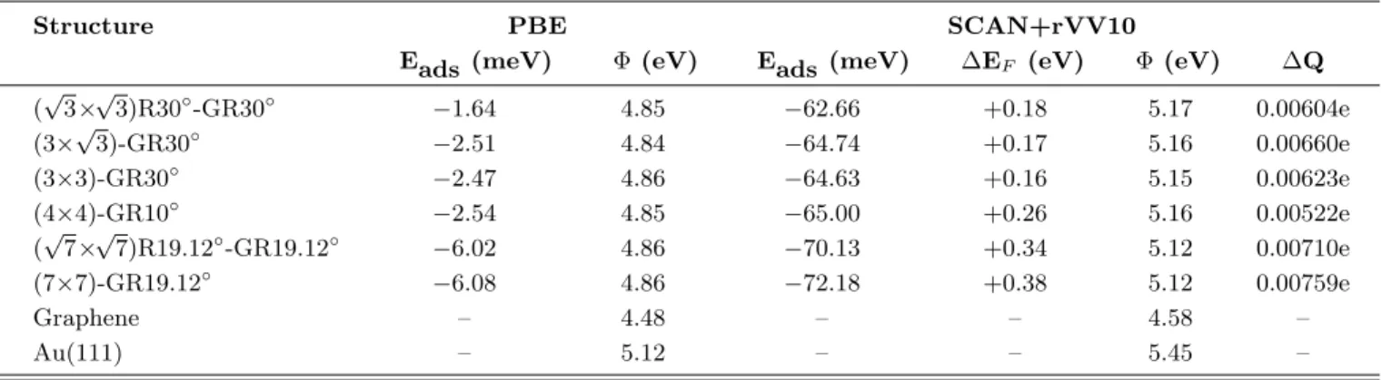
TABLE III. Average adsorption energy per C atom (Eads) , the work function of graphene, Au(111) and graphene coated
gold surface (Φ), the shift of the Dirac point of graphene with respect to the Fermi energy of the Au(111)/G system (∆EF),
the amount of charge (per C atom) displaced from graphene to gold (∆Q), calculated using the PBE and SCAN+rVV10 DFT functionals. Labeling of common structures of graphene and gold was made with respect to the surface unit cell of Au(111).
Structure PBE SCAN+rVV10
Eads (meV) Φ (eV) Eads (meV) ∆EF (eV) Φ (eV) ∆Q
(√3×√3)R30◦-GR30◦ −1.64 4.85 −62.66 +0.18 5.17 0.00604e (3×√3)-GR30◦ −2.51 4.84 −64.74 +0.17 5.16 0.00660e (3×3)-GR30◦ −2.47 4.86 −64.63 +0.16 5.15 0.00623e (4×4)-GR10◦ −2.54 4.85 −65.00 +0.26 5.16 0.00522e (√7×√7)R19.12◦-GR19.12◦ −6.02 4.86 −70.13 +0.34 5.12 0.00710e (7×7)-GR19.12◦ −6.08 4.86 −72.18 +0.38 5.12 0.00759e Graphene – 4.48 – – 4.58 – Au(111) – 5.12 – – 5.45 –
FIG. 3. Comparison of the adsorption energy (per C atom) profiles, calculated with different XC functionals, as a func-tion of the interlayer distance between the graphene layer and the gold (111)-(4×4) surface.
gold surface. [12, 79] In order to show the role of the vdW effects on the estimated values, we obtained the adsorption energy (per C atom) profiles as a function of the graphene/Au(111) interlayer distance using different XC functionals as shown in Fig. 3. In these calculations, the distance of graphene monolayer from the gold surface was changed stepwise and no relaxation was performed. The PBE functional severely underestimates the adsorp-tion energy. The standard GGA funcadsorp-tionals are not suit-able for chemisorption on metal systems either. For in-stance, even though the interaction between graphene and Ni(111) show a chemisorption behavior, PBE results suggest physisorption.[52] The SCAN and LDA function-als give a relatively better but not sufficiently strong in-teraction between graphene and gold substrate. When the SCAN functional is supplemented with the rVV10 vdW corrections, a significant improvement can be ob-tained on both the adsorption energy and the equilibrium distance.
In addition, the adsorption energy profile for the PBE functional gets almost insensitive to interlayer distance after ∼4.2 ˚A. Therefore, the PBE-predicted heights do not show a correlation with the strain ratios of graphene on gold. On the other hand, vdW-DFT results indicate a strong correlation between the height and the strain ratios as seen in Table. II. The factors mentioned above necessitates the inclusion of dispersive forces in the the-oretical calculations involving weakly interacting layered materials like graphene/Au(111).
Calculated adsorption energies per carbon atom are given in Table III. The PBE functional tends to un-derestimate the binding to a few meVs due to lack of long-range dispersive interactions as expected. The ad-sorption energies of a single layer graphene on the gold surface given by Zheng et al.[58] for the PBE functional are in excellent agreement with our results in Table III. On the other hand, vdW corrections bring a signifi-cant improvement over the energy related estimations. The interaction of graphene on the metal is relatively weak with Eads=−62.66 meV at the (
√
3 ×√3))R30◦ -GR30◦ superstrucutre and gets stronger with the in-creasing supercell size up to Eads=−72.18 meV at the
(7×7)-GR19.12◦ superstructure. The latter adsorption energy is in good agreement with a previous result ob-tained using DFT-D3 method.[79] Depending on the choice of the vdW functional scheme, the correspond-ing estimations may slightly vary. Our adsorption en-ergy values calculated using the SCAN+rVV10 func-tional gives a reasonable agreement with previous the-oretical estimations.[57, 58] The differences in the calcu-lated adsorption energies between computational stud-ies regarding the graphene/Au(111) system can be at-tributed to the use of different supercell structures and the vdW method. Another important factor appears to be the lack of rotational angular orientation of graphene on the gold surface in the previous studies. For instance, Tesch et al. considered the same alignment of graphene on both (2 × 2) and (7 × 7) graphene supercells which
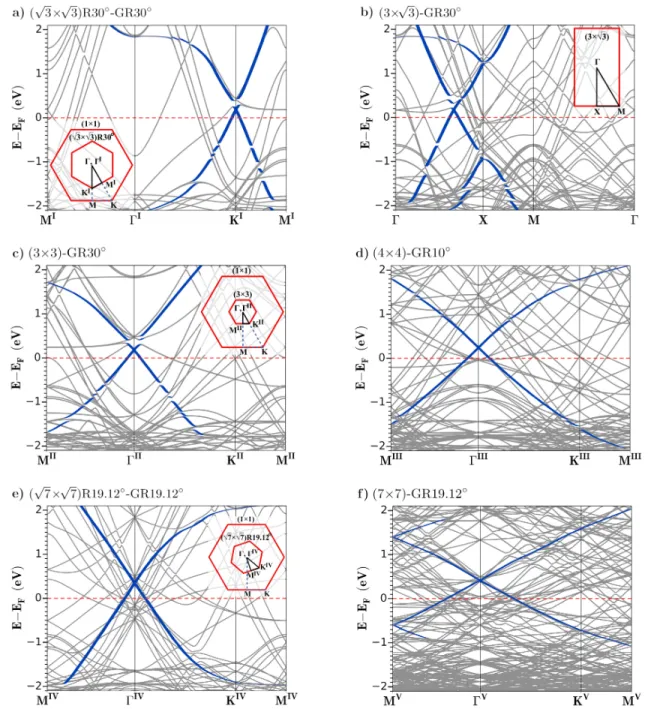
FIG. 4. Electronic band structures of graphene monolayer on Au(111) with identified common superstructures. The corre-sponding two-dimensional BZ and high-symmetry points are depicted in the insets. The contributions from graphene pzorbitals
are highlighted with blue color (thick dark bands). The energy values are given relative to the Fermi level (dashed lines) of each adsorption system.
correspond to (√3 ×√3)R30◦ and (6 × 6) gold surface supercells, respectively. In our optimization calculations graphene gets bulged on (6 × 6) gold surface therefore we did not include this case.
As a result, the graphene/metal interlayer distance is sensitive to the rotational angle/alignment of graphene monolayer on the metal surface. Moreover, adsorption energies also show an almost linear correlation with the interlayer distances computed with the SCAN-rVV10 functional.
B. Electronic Structures
The electronic band structures of corresponding com-mon graphene/Au(111) systems were obtained using the SCAN+rVV10 functional as shown in Fig. 4. The Bril-louin zone shapes, high symmetry points and the k-paths are shown in the insets. The size and the rotational align-ment of the corresponding BZ are also depicted relative to the hexagonal BZ of the (1 × 1) surface unit cell of gold.
It must be noted that the k-points (Γ, K , M, and X) are given with respect to the BZ of gold supercell. There is also inward folding of the BZ when the real space periodicity increases. Therefore, the conicals not always appear at the K point of graphene unitcell. In addition, the BZ shapes of hexagonal (3 × 3), (4 × 4), and (7 × 7) supercells are similar. They only get smaller in size with increasing supercell size in the real space.
The weak interfacial interactions represented by vdW corrections showed that the Dirac conicals are preserved. The linear dispersion of graphene bands within ±1 eV vicinity of the Dirac points of conicals can still be seen in all of the graphene adsorption orientations considered in this work. Moreover, graphene-metal interaction is weak such that it does not cause a band gap opening for the graphene monolayer. Then, the Dirac conicals differ in the position of the Fermi-level relative to the Dirac points. For a free-standing graphene, the Fermi-energy must be at the Dirac point. When graphene gets closer to the Au(111) surface a Fermi-level shift is observed. The downward shift of Fermi energy with respect to the Dirac point corresponds to a p-type doping of graphene monolayer.
The Fermi energy shift (with respect to the Dirac point) was found as +0.18 eV for√3 ×√3)R30◦-GR30◦ using the SCAN+rVV10 functional. This result is in good agreement with a previous value of +0.19 eV for the same structure.[46] Vanin et al. estimated a shift of +0.21 by using the vdW-DF method. Tesch et al.[79] synthesized graphene nanoflakes on Au(111) and re-ported a p-type doping with a Fermi energy shift of 0.24 ± 0.07 eV.[79] Similarly, Zheng et al. reported a Fermi-level shift of 0.230 eV for the bilayer graphene which is also reasonably close to the calculated values presented in this work. Our results for the R30◦ alignment struc-tures, (3×3)-GR30◦and (3×√3)-GR30◦, the shift values are similar because they all reflect essentially the same surface characteristics.
S lawi´nska et al.[42] used scanning tunneling spec-troscopy (STS) to show that Fermi-level shift ranges be-tween 0.25 and 0.55 eV on different p-type doping do-mains of graphene on the (111) surface of gold. Our results for the graphene/Au(111) physisorption systems, indicate that the shift changes with the rotational align-ment of graphene on the metal surface. The largest shift is calculated for the R19.12◦ alignment. The equilib-rium distances of the graphene/Au(111) structures are still large for a charge transfer from graphene to gold surface. Then, we calculated Bader charges on graphene and on metal slab before and after adsorption for each of the structures considered in this work. Calculated charge transfer values from the graphene monolayer to the gold substrate are very small and only slightly larger in the case of R19.12◦ structures. Hence, a charge transfer model may not fully explain the Fermi-level shift mecha-nism. Our results rather suggest a charge redistribution induced by graphene-metal interlayer interactions.
The change in the Fermi-level shift between different
common graphene/Au(111) geometries can be attributed to the rotational angle. Because, different angles cause different atomic coincidences of C atoms with the surface gold atoms. This also leads to a change in the ratio of the number of C atoms to the number of surface Au atoms (nC/Au) contained in the supercell. This ratio is
nC/Au=2.67, 2.63, and 2.57 at the rotational angles of
30◦, 10◦, and 19.12◦, respectively.
Another factor affecting the Fermi-level shift can be the work function of graphene/Au(111). Theoretical studies usually explain the shift as the difference between the work functions of metal surface and graphene mono-layer. Therefore, we calculated the work functions of common superstructures. The real space potential en-ergy profiles of the common hetero-layered structures were obtained along the [111] direction. Then the work function is the difference between the Fermi energy of the combined system and the vacuum level. Experimental work function of graphene and the gold surface is ∼4.62 eV.[81, 82] and 5.31 eV, respectively. Our SCAN+rVV10 functional estimation of 5.45 eV for the clean gold surface is in good agreement with recent theoretical values.[83] The PBE functional, on the other hand, gives a value of 5.12 eV for Au(111). Graphene monolayer is estimated to have a work function of 4.58 eV and 4.48 eV with and without the vdW-corrections, respectively. Calcu-lated work function values of graphene coated gold sur-face show a significant reduction relative to the that of the clean gold surface. Furthermore, our results does not show a meaningful trend to relate with the Fermi-energy shifts. On the other hand, the Φ values for different struc-tures all exhibit similar characteristics. Therefore, the work functions of graphene/Au(111) systems appear to be independent of graphene monolayer orientation on the gold surface. Interestingly, Song et al. recently reported that graphene in contact with Au gets an intermediate work function value and still dominantly show features of graphene.[81] The theoretically estimated work function values of the graphene/Au(111) superstructures assume an intermediate value and not pinned to the work func-tion of the metal.
IV. CONCLUSIONS
We have identified a number of small-sized common graphene/Au(111) superstructures by matching their corresponding supercells. Structural optimizations and electronic properties were obtained by performing DFT calculations. The weak interaction at graphene-gold in-terfaces necessitates the inclusion of vdW corrections. The standard GGA functionals tend to severely un-derestimate adsorption energies. The common geome-tries show different equilibrium distances between the graphene monolayer and the gold surface depending on the rotational orientation between them.
Graphene adsorption on gold does not destroy the Dirac conicals which still show linear dispersion within
±1 eV vicinity of the Dirac points. A change in the Fermi energy indicate p-type doping of graphene when adsorbed on the metal. Most importantly, we showed that the Fermi-level shifts depend on the rotational align-ment of the graphene on the gold surface.
Consequently, the results showed that the adsorption and electronic properties of graphene/Au(111) system are sensitive to the matching of graphene monolayer to the geometry of the gold surface at different rotational angles. This would allow a tunability of characteristics of potential applications based on graphene/metal lay-ered materials. The common superstructures identified in this study are useful and serve as building blocks to
construct and design novel hetero-layered materials in-volving graphene and Au(111).
ACKNOWLEDGEMENTS
This study was supported by Tubitak, The Scientific and Technological Research Council of Turkey, under Grant No. 116F174. The calculations were performed on the High Performance and Grid Computing Center (TRUBA). The authors also acknowledge financial sup-port from Balıkseir University under Grant No. BAP 2018/039.
[1] K. S. Novoselov, A. K. Geim, S. V. Morozov, D. Jiang, Y. Zhang, S. V. Dubonos, I. V. Grigorieva, and A. A. Firsov, Science 306, 666 (2004).
[2] K. S. Novoselov, A. K. Geim, S. V. Morozov, D. Jiang, M. I. Katsnelson, I. V. Grigorieva, S. V. Dubonos, and A. A. Firsov, Nature 438, 197 (2005).
[3] R. R. Nair, P. Blake, A. N. Grigorenko, K. S. Novoselov, T. J. Booth, T. Stauber, N. M. R. Peres, and A. K. Geim, Science 320, 13081308 (2008).
[4] K. V. Sreekanth, S. Zeng, J. Shang, K.-T. Yong, and T. Yu, Scientific Reports 2, 737 (2012).
[5] K. Bolotin, K. Sikes, Z. Jiang, M. Klima, G. Fudenberg, J. Hone, P. Kim, and H. Stormer, Solid State Commu-nications 146, 351355 (2008).
[6] C. L. Kane and E. J. Mele, Phys. Rev. Lett. 95, 226801 (2005).
[7] A. H. Castro Neto, F. Guinea, N. M. R. Peres, K. S. Novoselov, and A. K. Geim, Rev. Mod. Phys. 81, 109 (2009).
[8] S. Y. Zhou, G.-H. Gweon, A. V. Fedorov, P. N. First, W. A. de Heer, D.-H. Lee, F. Guinea, A. H. Castro Neto, and A. Lanzara, Nature Materials 6, 770 (2007). [9] L. Ci, L. Song, C. Jin, D. Jariwala, D. Wu, Y. Li, A.
Sri-vastava, Z. F. Wang, K. Storr, L. Balicas, and et al., Nature Materials 9, 430 (2010).
[10] P. A. Denis, Chemical Physics Letters 492, 251 (2010). [11] R. Balog, B. Jørgensen, L. Nilsson, M. Andersen,
E. Rienks, M. Bianchi, M. Fanetti, E. Lægsgaard, A. Baraldi, S. Lizzit, and et al., Nature Materials 9, 315319 (2010).
[12] J. Wintterlin and M.-L. Bocquet, Surface Science 603, 1841 (2009).
[13] M. Y. Han, B. ¨Ozyilmaz, Y. Zhang, and P. Kim, Phys. Rev. Lett. 98, 206805 (2007).
[14] Y.-C. Chen, D. G. de Oteyza, Z. Pedramrazi, C. Chen, F. R. Fischer, and M. F. Crommie, ACS Nano 7, 6123 (2013).
[15] M. H. Kang, L. O. Prieto Lpez, B. Chen, K. Teo, J. A. Williams, W. I. Milne, and M. T. Cole, ACS Applied Materials & Interfaces 8, 22506 (2016).
[16] T.-H. Han, Y. Lee, M.-R. Choi, S.-H. Woo, S.-H. Bae, B. H. Hong, J.-H. Ahn, and T.-W. Lee, Nature Photonics 6, 105 (2012).
[17] J. B. Oostinga, H. B. Heersche, X. Liu, A. F. Mor-purgo, and L. M. K. Vandersypen, Nature Materials 7,
151 (2007).
[18] X. Li, W. Cai, J. An, S. Kim, J. Nah, D. Yang, R. Piner, A. Velamakanni, I. Jung, E. Tutuc, S. K. Banerjee, L. Colombo, and R. S. Ruoff, Science 324, 1312 (2009). [19] A. Reina, X. Jia, J. Ho, D. Nezich, H. Son, V. Bulovic, M. S. Dresselhaus, and J. Kong, Nano Letters 9, 30 (2009).
[20] R. Nouchi, M. Shiraishi, and Y. Suzuki, Applied Physics Letters 93, 152104 (2008).
[21] O. Salihoglu, S. Balci, and C. Kocabas, Applied Physics Letters 100, 213110 (2012).
[22] K. Kim, J.-Y. Choi, T. Kim, S.-H. Cho, and H.-J. Chung, Nature 479, 338 (2011).
[23] S. Lin, Y. Lu, J. Xu, S. Feng, and J. Li, Nano Energy 40, 122 (2017).
[24] P. Merino, M. vec, A. L. Pinardi, G. Otero, and J. A. Martn-Gago, ACS Nano 5, 5627 (2011).
[25] J. M. Wofford, E. Starodub, A. L. Walter, S. Nie, A. Bostwick, N. C. Bartelt, K. Thrmer, E. Rotenberg, K. F. McCarty, and O. D. Dubon, New Journal of Physics 14, 053008 (2012).
[26] I. Pletikosi´c, M. Kralj, P. Pervan, R. Brako, J. Coraux, A. T. N’Diaye, C. Busse, and T. Michely, Phys. Rev. Lett. 102, 056808 (2009).
[27] S.-Y. Kwon, C. V. Ciobanu, V. Petrova, V. B. Shenoy, J. Bareo, V. Gambin, I. Petrov, and S. Kodambaka, Nano Letters 9, 3985 (2009).
[28] H. Vita, S. Bttcher, K. Horn, E. N. Voloshina, R. E. Ovcharenko, T. Kampen, A. Thissen, and Y. S. Dedkov, Scientific Reports 4 (2014).
[29] Y. S. Dedkov, A. M. Shikin, V. K. Adamchuk, S. L. Molodtsov, C. Laubschat, A. Bauer, and G. Kaindl, Phys. Rev. B 64, 035405 (2001).
[30] S. Marchini, S. G¨unther, and J. Wintterlin, Phys. Rev. B 76, 075429 (2007).
[31] V. M. Karpan, G. Giovannetti, P. A. Khomyakov, M. Ta-lanana, A. A. Starikov, M. Zwierzycki, J. van den Brink, G. Brocks, and P. J. Kelly, Phys. Rev. Lett. 99, 176602 (2007).
[32] M. Gao, Y. Pan, C. Zhang, H. Hu, R. Yang, H. Lu, J. Cai, S. Du, F. Liu, and H.-J. Gao, Applied Physics Letters 96, 053109 (2010).
[33] C. Enderlein, Y. S. Kim, A. Bostwick, E. Rotenberg, and K. Horn, New Journal of Physics 12, 033014 (2010).
[34] W. Moritz, B. Wang, M.-L. Bocquet, T. Brugger, T. Gre-ber, J. Wintterlin, and S. G¨unther, Phys. Rev. Lett. 104, 136102 (2010).
[35] A. Varykhalov, J. S´anchez-Barriga, A. M. Shikin, C. Biswas, E. Vescovo, A. Rybkin, D. Marchenko, and O. Rader, Phys. Rev. Lett. 101, 157601 (2008).
[36] P. W. Sutter, J.-I. Flege, and E. A. Sutter, Nature Ma-terials 7, 406 (2008).
[37] P. Sutter, J. T. Sadowski, and E. Sutter, Phys. Rev. B 80, 245411 (2009).
[38] Z. Klusek, P. Dabrowski, P. Kowalczyk, W. Kozlowski, W. Olejniczak, P. Blake, M. Szybowicz, and T. Runka, Applied Physics Letters 95, 113114 (2009).
[39] D. Eom, D. Prezzi, K. T. Rim, H. Zhou, M. Lefenfeld, S. Xiao, C. Nuckolls, M. S. Hybertsen, T. F. Heinz, and G. W. Flynn, Nano Letters 9, 2844 (2009).
[40] G. Giovannetti, P. A. Khomyakov, G. Brocks, V. M. Karpan, J. van den Brink, and P. J. Kelly, Phys. Rev. Lett. 101, 026803 (2008).
[41] J. S lawi´nska, P. Dabrowski, and I. Zasada, Phys. Rev. B 83, 245429 (2011).
[42] J. S lawi´nska, I. Wlasny, P. Dabrowski, Z. Klusek, and I. Zasada, Phys. Rev. B 85, 235430 (2012).
[43] G. Bertoni, L. Calmels, A. Altibelli, and V. Serin, Phys. Rev. B 71, 075402 (2005).
[44] I. Hamada and M. Otani, Phys. Rev. B 82, 153412 (2010).
[45] C. Gong, G. Lee, B. Shan, E. M. Vogel, R. M. Wallace, and K. Cho, Journal of Applied Physics 108, 123711 (2010).
[46] P. A. Khomyakov, G. Giovannetti, P. C. Rusu, G. Brocks, J. van den Brink, and P. J. Kelly, Phys. Rev. B 79, 195425 (2009).
[47] M. H. Kang, S. C. Jung, and J. W. Park, Phys. Rev. B 82, 085409 (2010).
[48] R. Brako, D. okevi, P. Lazi, and N. Atodiresei, New Journal of Physics 12, 113016 (2010).
[49] S. M. Kozlov, F. Vi˜nes, and A. G¨orling, The Journal of Physical Chemistry C 116, 7360 (2012).
[50] J. C. W. Swart, E. van Steen, I. M. Ciobc, and R. A. van Santen, Phys. Chem. Chem. Phys. 11, 803 (2009). [51] B. Uchoa, C.-Y. Lin, and A. H. Castro Neto, Phys. Rev.
B 77, 035420 (2008).
[52] M. Fuentes-Cabrera, M. I. Baskes, A. V. Melechko, and M. L. Simpson, Physical Review B 77, 035405 (2008). [53] M. M. Ugeda, D. Fern´andez-Torre, I. Brihuega, P. Pou,
A. J. Mart´ınez-Galera, R. P´erez, and J. M. G´ omez-Rodr´ıguez, Phys. Rev. Lett. 107, 116803 (2011). [54] Z. Xu and M. J. Buehler, Journal of Physics: Condensed
Matter 22, 485301 (2010).
[55] M. Vanin, J. J. Mortensen, A. K. Kelkkanen, J. M. Garcia-Lastra, K. S. Thygesen, and K. W. Jacobsen, Phys. Rev. B 81, 081408(R) (2010).
[56] W. Zhao, S. M. Kozlov, O. Hfert, K. Gotterbarm, M. P. A. Lorenz, F. Vies, C. Papp, A. Grling, and H.-P. Steinrck, The Journal of Physical Chemistry Letters 2, 759 (2011).
[57] M. Andersen, L. Hornekær, and B. Hammer, Phys. Rev. B 86, 085405 (2012).
[58] J. Zheng, Y. Wang, L. Wang, R. Quhe, Z. Ni, W.-N. Mei, Z. Gao, D. Yu, J. Shi, and J. Lu, Scientific Reports 3, 2081 (2013).
[59] P. A. DiMilla, J. P. Folkers, H. A. Biebuyck, R. Haerter, G. P. Lopez, and G. M. Whitesides, Journal of the Amer-ican Chemical Society 116, 2225 (1994).
[60] A. Kumar, H. A. Biebuyck, and G. M. Whitesides, Lang-muir 10, 1498 (1994).
[61] C. B. Gorman, H. A. Biebuyck, and G. M. Whitesides, Langmuir 11, 2242 (1995).
[62] M. Mrksich, L. E. Dike, J. Tien, D. E. Ingber, and G. M. Whitesides, Experimental cell research 235, 305 (1997). [63] H. Yamada, H. Imahori, Y. Nishimura, I. Yamazaki,
T. K. Ahn, S. K. Kim, D. Kim, and S. Fukuzumi, Jour-nal of the American Chemical Society 125, 9129 (2003). [64] J. H. Sch¨on, H. Meng, and Z. Bao, Nature 413, 713
(2001).
[65] N. K. Chaki and K. Vijayamohanan, Biosensors and Bio-electronics 17, 1 (2002).
[66] R. Lao, S. Song, H. Wu, L. Wang, Z. Zhang, L. He, and C. Fan, Analytical chemistry 77, 6475 (2005).
[67] X. Xie, K. Zhao, X. Xu, W. Zhao, S. Liu, Z. Zhu, M. Li, Z. Shi, and Y. Shao, The Journal of Physical Chemistry C 114, 14243 (2010).
[68] B. Li, M. Famili, E. Pensa, I. Grace, N. J. Long, C. Lam-bert, T. Albrecht, and L. F. Cohen, Nanoscale 10, 19791 (2018).
[69] H. Yan, K. T. Narasimha, J. Denlinger, F. H. Li, S.-K. Mo, J. N. Hohman, J. E. Dahl, R. M. Carlson, B. A. Tkachenko, A. A. Fokin, et al., Nano letters 18, 1099 (2018).
[70] G. Kresse and J. Hafner, Phys. Rev. B 47, 558 (1993). [71] G. Kresse and J. Furthm¨uller, Phys. Rev. B 54, 11169
(1996).
[72] G. Kresse and D. Joubert, Phys. Rev. B 59, 1758 (1999). [73] P. E. Bl¨ochl, Phys. Rev. B 50, 17953 (1994).
[74] J. Sun, A. Ruzsinszky, and J. P. Perdew, Phys. Rev. Lett. 115, 036402 (2015).
[75] S. Nie, N. C. Bartelt, J. M. Wofford, O. D. Dubon, K. F. McCarty, and K. Th¨urmer, Phys. Rev. B 85, 205406 (2012).
[76] O. A. Vydrov and T. Van Voorhis, The Journal of Chem-ical Physics 133, 244103 (2010).
[77] H. Peng, Z.-H. Yang, J. P. Perdew, and J. Sun, Phys. Rev. X 6, 041005 (2016).
[78] R. W. G. Wyckoff, Interscience Publishers, New York, 2nd edn (1958).
[79] J. Tesch, P. Leicht, F. Blumenschein, L. Gragnaniello, M. Fonin, L. E. Marsoner Steinkasserer, E. Paulus, Beate Voloshina, and Y. Dedkov, Scientific Reports 6, 23439 (2016).
[80] G. Zhao, X. Li, M. Huang, Z. Zhen, Y. Zhong, Q. Chen, X. Zhao, Y. He, R. Hu, T. Yang, R. Zhang, C. Li, J. Kong, J.-B. Xu, R. S. Ruoff, and H. Zhu, Chem. Soc. Rev. 46, 4417 (2017).
[81] S. M. Song, J. K. Park, O. J. Sul, and B. J. Cho, Nano Letters 12, 3887 (2012).
[82] H. Yuan, S. Chang, I. Bargatin, N. C. Wang, D. C. Riley, H. Wang, J. W. Schwede, J. Provine, E. Pop, Z.-X. Shen, P. A. Pianetta, N. A. Melosh, and R. T. Howe, Nano Letters 15, 6475 (2015).
[83] A. Patra, J. E. Bates, J. Sun, and J. P. Perdew, Pro-ceedings of the National Academy of Sciences 114, E9188 (2017).