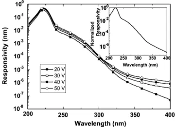
Deep-ultraviolet Al0.75Ga0.25N photodiodes with low cutoff wavelength
Tam metin
Şekil
Benzer Belgeler
derdimendiŋ dâmânı 31b, 1-2 Belirli isim tamlaması cihânıŋ niómetindeŋ 26a, 9 Belirli isim tamlaması iliŋ kâşânesinden 26a, 10 Belirli isim tamlaması kendü miøkdârın
In the trade with the western countries, Hungary should have focus on the commodity groups that gave the country comparative advantage like industrial raw
The collection of all patches extracted from all images for a single attribute is then given to CMAP to obtain clusters which are likely to capture different characteristics of
If we go beyond state-centrism and security professionalism to explore the plurality of the politics of security in former Yugoslavia, and if we expand our analytical focus to
After admittance of Haga with the Sultan and just before the granting of the Dutch capitulations, Halil Paşa sent a letter to the States General and Prince Maurice
If there is evidence that real interest rates move in response to expected inflation, then inflationary movements have not been totally absorbed in nominal
Reprinted in Primers for Prudery: Sexual Advice to Victorian America, edited by Ronald G.. Baltimore: Johns Hopkins University
In partic- ular, as shown in chapter 5, the structural undirected networks in Alzheimer’s patients show abnormal organization that is manifested through changes in the
