i
THE MECHANICAL CHARACTERIZATION OF
TWO-DIMENSIONAL MATERIALS (WS
2, MoS
2, AND GRAPHENE) AND
THE EFFECT OF DEFECTS ON YOUNG`S MODULUS OF CVD
GROWN SINGLE-LAYER GRAPHENE
A THESIS SUBMITTED TO
THE GRADUATE SCHOOL OF ENGINEERING AND SCIENCE OF BILKENT UNIVERSITY
IN PARTIAL FULFILLMENT OF THE REQUIREMENTS FOR THE DEGREE OF
MASTER OF SCIENCE IN
MATERIALS SCIENCE AND NANOTECHNOLOGY
By
Begimai Adilbekova November 2017
ii
THE MECHANICAL CHARACTERIZATION OF TWO-DIMENSIONAL
MATERIALS (WS
2, MoS
2, AND GRAPHENE) AND THE EFFECT OF
DEFECTS ON YOUNG`S MODULUS OF CVD GROWN
SINGLE-LAYER GRAPHENE
By Begimai Adilbekova November 2017
We certify that we have read this thesis and that in our opinion it is fully adequate, in scope and in quality, as a thesis for the degree of Master of Science.
___________________________________ Aykutlu Dana (Supervisor)
___________________________________ Raşit Turan (METU)
___________________________________ Seymur Jahangirov
Approved for the Graduate School of Engineering and Science:
___________________________________ Ezhan Karaşan
i
ABSTRACT
THE MECHANICAL CHARACTERIZATION OF TWO-DIMENSIONAL
MATERIALS (WS2, MOS2, AND GRAPHENE) AND THE EFFECT OF
DEFECTS ON YOUNG`S MODULUS OF CVD GROWN SINGLE-LAYER GRAPHENE
Begimai Adilbekova
M.S in Materials Science and Nanotechnology Supervisor: Aykutlu Dana
2017
With the first isolation of graphene two-dimensional (2D) materials attracted the enormous interest of many researchers. Owing to extraordinary properties and atomic thickness 2D materials have many applications in gas detection, electrodes, energy storage devices, field effect devices, sensors, photodetectors, solar cells, nanocomposites, actuators/ resonators, biological membranes,cancer detectors, piezoresistive pressure sensors, gas impermeable membranes, gas or liquid separation. Despite the atomic thickness, the gapless character of the graphene limits its applications in modern electronic devices. There are two strategies for solving the problem, first one is to open the band-gap in graphene and second is to explore new 2D materials. Generation of defects and applying an electrical field can increase the band-gap of graphene but defects can affect other properties of it.
Therefore, there is a need for new analogs and transition metal dichalcogenides (TMDs) are the most promising ones. TMDs drew the attention of many researchers because of the remarkable electronic and optical properties. TMD
ii
materials exhibit a semiconducting nature owing to the presence of the band-gap, which is essential for the logical operations. Besides electronic properties, the mechanical properties( Young`s Modulus) play a significant role in applications of 2D materials. 2D materials are most promising candidates for flexible electronic devices, which received enormous interest in recent years. But the applied strain and other external forces can modify the structure of crystalline graphene and TMDs, consequently affect the performance and lifetime of devices.
In this work, we aimed to measure the Young`s Modulus of graphene, MoS2 film,
MoS2 and WS2 flakes with an Atomic Force Microscope (AFM). In addition, we
sought the relation between the defect intensity and Young`s Modulus of graphene. The defects in graphene were generated by Ga+ with different doses in Focused Ion Beam (FIB).
We found Young`s Moduli of graphene, MoS2 film, MoS2 and WS2 flakes to be
270 N/m, 330 N/m, 90 N/m and 140 N/m, respectively. These values are lower than those given in a literature, what might be caused by the pre-existence of unwanted defects. Also, it appeared that the introduction of defects leads to the fall in Young`s Modulus values of the graphene.
Keywords: 2D materials, graphene, MoS2 film, MoS2 flakes,WS2 flakes, Young`s
iii
ÖZET
İKİ BOYUTLU MALZEMELERİN (WS2, MOS2 VE GRAFEN) MEKANİK
KARAKTERİZASYONU VE TEK TABAKALI GRAFENİNİN YOUNG KATSAYISININ KUSUR YOĞUNLUĞU İLE DEĞİŞİMİ
Begimai Adilbekova
Malzeme Bilimi ve Nanoteknoloji bölümü Yüksek Lisans Tez danışmanı: Aykutlu Dana
2017
Grafenin ilk izolasyonu ile iki boyutlu (2B) malzemelerin bir çok araştırmacının ilgisini çekmiştir. Olağanüstü özellikleri ve atom kalınlığı nedeniyle 2B malzemelerin gaz algılama, elektrotlar, enerji depolama cihazları, alan etkili cihazlar, sensörler, fotodetektörler, güneş pilleri, nanokompozitörler, aktüatörler / rezonatörler, biyolojik membranlar, kanser dedektörleri, piezoresistif basınç sensörleri, gaz geçirimez zarlar, gaz veya sıvı ayrımı gibi uygulamaları vardır. Atomik kalınlığa rağmen, grafenin bant aralıgının olmaması, modern elektronik cihazlardaki uygulamalarını sınırlar. Bu sorunu çözmek için iki strateji vardır; birincisi, grafende bant aralığını açmaktır ve ikincisi de yeni 2B malzemelerin keşfetmektir. Kusurların üretilmesi ve bir elektrik alanının uygulanması grafenin bant aralığını artırabilir, ancak üretilen kusurlar diğer özelliklerini de etkileyebilir. Bu nedenle, yeni analog malzemelere ihtiyaç vardır ve geçiş metali kalkojenleri (TMD) en umut verici malzemelerdir. TMD'ler elektronik ve optik özelliklerinden dolayı birçok araştırmacının dikkat çekmiştir. TMD malzemeleri mantıksal işlemler için gerekli olan bant aralığının varlığı nedeniyle yarı iletken bir yapı sergilemektedir.
iv
Elektronik özelliklerin yanı sıra, 2B malzemelerin mekanik özellikler (Young Modülü) onların uygulamalarında önemli bir rol oynamaktadır. Ve 2D malzemeler son yıllarda büyük ilgi gören esnek elektronik cihazlar için en umut verici adayları olmaları onların mekanik özelliklerinin önemini arttırmaktadır. Çünkü uygulanan gerginlik ve diğer dış kuvvetler grafen ve TMD'lerin krıstal yapısını değiştirebilir ve sonuç olarak cihazların performansını ve ömrünü etkiler.
Bu çalışmada grafenin, MoS2 filmin, MoS2 ve WS2 parçalarının Young katsayısını
Atomik Kuvvet Mikroskobu (AFM) araçıyla ölçmeyi amaçladık. Buna ek olarak, kusur yoğunluğu ile grafenin Young katsayısı arasındaki ilişkiyi araştırdık.Farklı yoğunluklarda kusur oluşturmak için grafeni Focused Ion Beam (FIB) cıhazında değişik dozlardaki Ga + iyonlarına maruz bıraktık.
Sonuç olarak grafenin, MoS2 filminin, MoS2 ve WS2 parçalarının Young
Modüllerini sırasıyla 270 N / m, 330 N / m, 90 N / m ve 140 N / m olarak bulduk. Bu değerlerin literatürde verilenlerden daha düşük olması istenmeyen kusurların varlığından kaynaklanmış olabilir. Aynı şekilde grafende olusturulan kusurların yoğunluğuyla grafen'in Young Modülünün düstügü gözlemlenmiştir.
Anahtar Kelimeler: 2D malzemeler, grafen, MoS2 film, MoS2 parçaları,WS2 parçalarıYoung Modülü, kusurlar.
v
ACKNOWLEDGEMENTS
I would like to express my gratitude and appreciation to my supervisor Asst. Prof. Dr. Aykutlu Dana for his great guidance, encouragements, advices, and help. It was a great pleasure to work with him and attain valuable experiences. Also, I would like to especially thank other members of my thesis committee.
I had a chance to work with Dr. Kemal Celebi and I learned a lot from him, so I am deeply grateful for his guidance and help.
I`d like to thank Kakenov Nurbek and Dr. Coskun Kocabas for the graphene supply, Dr. Seymur Jahangirov and his students for the DFT calculations.
I thank all engineers, UNAM members for their help. Also, I`d like to thank my friends, especially, Mehmet Yurtseven, Gamze Torunoglu, Abdullah Onen, Abtin Sateh, Timur Ashirov, Doolos Aibek uulu for their help and support.
Finally, my special gratitude to my family for the great support, motivation, and encouragement.
vi
TABLE OF CONTENTS
ABSTRACT ...II ÖZET ... III ACKNOLEDGEMENTS ... V TABLEOFCONTENTS ... VI LISTOFFIGURES ... IX CHAPTER 1 ... 1 INTRODUCTION ... 1 1.1 HISTORICAL BACKGROUND ... 1 1.2 LITERATURE OVERVIEW ... 4 1.2.1 PROPERTIES ... 41.2.1.1 ELECTRICAL AND ELECTRONIC PROPERTIES ... 4
1.2.1.2 OPTICAL PROPERTIES ... 6 1.2.1.3 THERMAL PROPERTIES ... 7 1.2.1.4 CHEMICAL PROPERTIES ... 8 1.2.1.5 MECHANICAL PROPERTIES ... 8 1.2.1.6 YOUNG`S MODULUS ... 9 1.2.2 DEFECTS IN GRAPHENE ... 12
STONE-WALES (SW) DEFECT ... 12
SINGLE VACANCIES (SV) ... 13
MULTIPLE OR DOUBLE VACANCIES (DV) ... 14
ADATOMS ... 14
SUBSTITUTIONAL IMPURITIES ... 16
ONE-DIMENSIONAL DEFECTS ... 16
EDGES DEFECTS ... 17
vii
CHAPTER 2 ... 19
MATERIALS AND METHODS ... 19
2.1 GRAPHENE SYNTHESIS ... 19
2.1.1 EXFOLIATION AND CLEAVAGE ... 19
2.1.2 PLASMA-INDUCED LAYER-BY-LAYER THINNING ... 20
OXYGEN PLASMA ... 20
HYDROGEN PLASMA ... 20
OTHER PLASMAS ... 21
2.1.3 CHEMICAL VAPOR DEPOSITION (CVD) ... 21
THERMAL DECOMPOSITION OF SIC ... 21
PLASMA ENHANCED CVD GROWTH OF GRAPHENE ... 22
CHEMICAL VAPOR DEPOSITION (CVD) ... 22
2.2 TMDS SYNTHESIS ... 24
2.2.1 EXFOLIATION ... 25
2.2.2 CVD GROWTH ... 26
2.3 CHARACTERIZATION METHODS ... 27
2.3.1 OPTICAL IMAGING ... 28
2.3.2 TRANSMISSION ELECTRON MICROSCOPY (TEM) ... 28
2.3.3 SCANNING ELECTRON MICROSCOPY (SEM) ... 29
2.3.4 RAMAN SPECTROSCOPY ... 29
2.3.5 ATOMIC FORCE MICROSCOPY (AFM) ... 30
2.4 MEASUREMENT OF YOUNG`S MODULUS OF 2D MATERIALS ... 31
2.4.1 RAMAN-BASED MEASUREMENTS ... 31
2.4.2 NANOINDENTATION ... 33
2.5 GENERATION OF DEFECTS IN GRAPHENE ... 35
2.5.1 GRAPHENE CRYSTAL GROWTH ... 36
2.5.2 IRRADIATION WITH ENERGETIC PARTICLES ... 36
2.5.3 CHEMICAL TREATMENT ... 36
CHAPTER 3 ... 37
viii
3.1 GRAPHENE PREPARATION ... 37
3.1.1 CHARACTERIZATION OF GRAPHENE AND TMDS ... 41
3.1.2 GENERATION OF DEFECTS IN SUSPENDED GRAPHENE ... 42
CHAPTER 4 ... 43
RESULTS AND DISCUSSION ... 43
4.1 CHARACTERIZATION OF GRAPHENE ... 43
4.1.1 CHARACTERIZATION BY THE OPTICAL MICROSCOPY,RAMAN SPECTROSCOPY AND SEM ... 43
4.1.2 CHARACTERIZATION BY TEM ... 51
4.1.3 CHARACTERIZATION BY AFM ... 54
4.1.4 THE MEASUREMENT OF YOUNG`S MODULUS ... 57
4.1.5 THE EFFECT OF DEFECTS ON YOUNG`S MODULUS ... 59
4.2 CHARACTERIZATION OF TMDS (MOS2 FILM,MOS2 AND WS2 FLAKES) ... 72
4.2.1 CHARACTERIZATION BY OPTICAL MICROSCOPY,RAMAN SPECTROSCOPY AND SEM 72 CHARACTERIZATION BY AFM ... 81
THE MEASUREMENT OF YOUNG`S MODULUS ... 85
4.2 CONCLUSION ... 90
BIBLIOGRAPHY ... 92
APPENDICES ... 98
APPENDIX 1 ... 98
ix
LIST OF FIGURES
Figure 1. Schematic illustration of a) single layer graphene`s structure, b) stacked graphene sheets (graphite) structure. ... 2 Figure 2. Schematic illustration of band gap for a) single-layer graphene, b) double-layer graphene, c) double layer graphene when an electrical field
perpendicular to graphene sheets is applied. ... 5 Figure 3. Schematic stress-strain diagram showing the linear and nonlinear behavior of a material. ... 11 Figure 4. Schematic Stone-Wales defect (77-55) in graphene lattice. ... 13 Figure 5. Schematic defects (a) Single vacancy defect and (b) Atomic structures of reconstructed single vacancy defect V1 (5-9). ... 13
Figure 6. Schematic illustration of defects (a) Double vacancy defect, (b) atomic structures of reconstructed double vacancy defect V2 (5-8-5, (c) atomic structures
of reconstructed double vacancy defect V2 (555-777). ... 14
Figure 7. Schematic illustration of single carbon adatom (a,c) in the bridge; (b,d) in the dumbbell configuration. ... 15 Figure 8. Schematic illustration of noncarbon (metal-green) atom (a) on single vacancy (b) on double vacancy. Metal atoms use the third dimension. ... 16 Figure 9. Schematic illustration of Force-distance curve. ... 31 Figure 10. Schematic illustration of the experimental setup used for
measurement of Young`s modulus by Raman... 32 Figure 11. (a)The force-displacement curve, (b) The curve fitting. ... 34 Figure 12. Schematic illustration of the experimental setup used for
measurement of 2D material`s Young`s modulus by AFM. ... 35 Figure 13. SiN2/SiO2 frame. a) Frontside b) Backside. ... 39
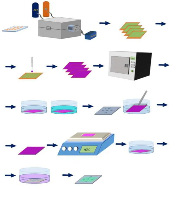
Figure 14. Sample preparation. Graphene samples grown on Cu foil pieces in CVD are covered by photoresist and baked for 16 hours at 60˚ in the furnace.
x
Samples are slowly cooled in air and Cu is etched by (NH4)2S2O8 or HNO3
solution, and fished out onto prepared clean SiO2/SiN /Si frames.
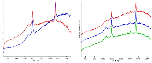
Graphene/photoresist are dried in air and baked at 90˚C for few seconds. Finally, the photoresist is removed by acetone (96-98%) and rinsed with IPA several times. ... 40 Figure 15. Optical microscopy images of (a) graphene on a SiO2/Si3N4/Si ,(b-c)
suspended graphene on a holey SiO2/Si3N4/Si frame. ... 44
Figure 16. ESEM images of graphene transferred onto a holey SiO2/Si3N4/Si
frame. Cu etch was made with a) HNO3 and b) (NH4)2S2O8. ... 45
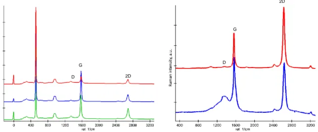
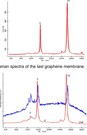
Figure 17. Suspended graphene on holey SiO2/ SiN/ Si washed with acetone once. ... 45 Figure 18. Raman spectroscopy of graphene on a holey substrate after acetone wash (once). ... 46 Figure 19.Suspended graphene on holey SiO2/ SiN/ Si washed with acetone twice. ... 47 Figure 20. Raman spectroscopy of graphene on a holey substrate after acetone wash (twice). ... 48 Figure 21(a-d). The ESEM images of Suspended graphene sample. ... 49 Figure 22. The Raman spectra of the last graphene membrane. ... 50 Figure 23.Comparison of Raman spectroscopy results of graphene samples washed with acetone once (blue) and the last sample (red). ... 50 Figure 24(a,b). Raman spectra of suspended monolayer graphene. ... 51 Figure 25. Raman spectra of suspended monolayer graphene with different strain values. ... 51 Figure 26, (a-c) Electron diffraction patterns of single layer suspended graphene from three different points. ... 52 Figure 27. (a-f)TEM images of a suspended graphene (arrows indicate: red-tears/holes, yellow-contaminations/residues, blue-grain boundaries, green-folds, black-chain consisting of few atoms). ... 53
xi
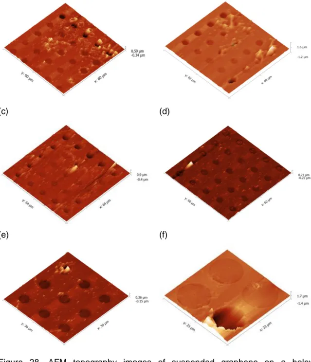
Figure 28. AFM topography images of suspended graphene on a holey
SiO2/Si3N4/Si frame (a-b) After the single acetone wash, (c-f) After the double acetone wash. ... 55 Figure 29 (a-f). The tapping mode AFM imaging (topography) of individual holes with suspended graphene. ... 56 Figure 30. The 2D Young`s Modulus distribution and Force Map (inset) of
graphene before the ion bombardment. ... 58 Figure 31. The 2D Young`s Modulus distribution of graphene after the ion
bombardment with a dose of 4.345 pA/s. ... 59 Figure 32. The 2D Young`s Modulus distribution of graphene after the ion
bombardment with a dose of 10.863 pA/s. ... 60 Figure 33. The 2D Young`s Modulus distribution of graphene after the ion
bombardment with a dose of 11.949 pA/s. ... 61 Figure 34. The 2D Young`s Modulus distribution of graphene after the ion
bombardment with a dose of 21.725 pA/s. ... 63 Figure 35. The 2D Young`s Modulus distribution of graphene after the ion
bombardment with a dose of 43.450 pA/s. ... 64 Figure 36. The 2D Young`s Modulus distribution of graphene after the ion
bombardment with a dose of 74.680 pA/s ... 65 Figure 37. The 2D Young`s Modulus distribution of graphene after the ion
bombardment with a dose of 109.984 pA/s. ... 66 Figure 38 (a-i). The 2D Young`s Modulus distribution of graphene after the ion bombardment with a dose of 127.635 pA/s. ... 67 Figure 39. The distribution of 2D Young`s Modulus of graphene after ion
irradiation with dose of (a) 0 pA/s, (b) 4.345 pA/s, (c) 10.863 pA/s, (d)11.949 pA/s, (e)21.725 pA/s, (f) 43.450 pA/s, (g) 74.450 pA/, (h)109.984 pA/s, (i)
127.635 pA/s. ... 68 Figure 40. The comparison of distributions of 2D Young`s Modulus of graphene after ion irradiation with different doses. ... 69 Figure 41. The change of 2D Young`s Modulus of graphene with the Ga+ ion irradiation dose. ... 70
xii
Figure 42. The change of 2D Young`s Modulus of graphene with the Ga+ ion
irradiation dose. ... 71
Figure 43.Optical image of suspended (a) MoS2 film, (b-c) MoS2 flakes. ... 73
Figure 44 (a-c). The optical image of suspended WS2 flakes. ... 73
Figure 45. ESEM images of the MoS2 film (3 layers) on a holey substrate... 74
Figure 46. ESEM images of MoS2 flakes on a holey substrate. ... 75
Figure 47 (a-c). ESEM images of WS2 flakes on a holey substrate. ... 75
Figure 48. Raman spectra of the MoS2 film (3L). ... 76
Figure 49. PL of MoS2 film taken by Raman Spectroscopy. ... 77
Figure 50. (a) The Raman Spectra and (b) Mapping of MoS2 flakes ... 77
Figure 51. The Raman spectra comparison of MoS2 with different thicknesses. 78 Figure 52. (a) The PL spectra and (b) PL mapping of MoS2 flakes. ... 79
Figure 53. (a) The Raman spectra and (b) Raman mapping of WS2 flakes. ... 80
Figure 54. (a) The PL spectra and (b) PL mapping of WS2 flakes. ... 80
Figure 55. AFM images of the MoS2 film. ... 82
Figure 56. AFM images of MoS2 flakes. ... 83
Figure 57. AFM images of WS2 flakes. ... 84
Figure 58. The 2D Young`s Modulus of MoS2 film. ... 85
Figure 59. The 2D Young`s Modulus of MoS2 flakes. ... 86
Figure 60. The 2D Young`s Modulus of WS2 flakes. ... 87
Figure 61. The distribution of 2D Young`s Modulus of MoS2 film. ... 88
Figure 62. The 2D Young`s Modulus distribution of MoS2 flakes. ... 88
Figure 63. The 2D Young`s Modulus distribution of WS2 flakes. ... 89
Figure 64. Comparison of the 2D Young`s Modulus distribution of the MoS2 film, WS2, and MoS2 flakes. ... 90
Figure 65. (a) Top view of the structures of graphene, (b) single defect in 2×2×1 and (c) 3×3×1 graphene. ... 99
Figure 66. Force-Map of graphene. ... 100
Figure 67. (a)Force-map and (b) Histogram of distribution of 2D Young`s Modulus. ... 104
1
CHAPTER 1
Introduction
1.1 Historical Background
From the beginning of the XXI century with an exploration of graphene in 2004, numerous studies are focused on two-dimensional material like graphene, WSe2,
MoS2, MoSe2, WSe2. Before Novoselov and Geim (2004) isolated pristine
graphene for the first time by mechanical cleavage from the bulk graphite, which was used for thousands of years, according to the Mermin-Wagner theorem it was believed that two-dimensional crystals are not stable because of long-wavelength fluctuations and to obtain graphene was an uphill task [1][2][3][4][5][6].
Graphene is sp2-bonded carbon sheet consisting of aromatic hexagonal
rings with a bond length of 0.142 nm Figure 1(a), and stacked layers of graphene form graphite by weak van der Waals (vdW) interactions [3][7][8][9][5] as shown in Figure 1(b). The conduction and weak interactions are caused by partially filled π orbitals [10].
2
(a) (b)
Figure 1. Schematic illustration of a) single layer graphene`s structure, b) stacked graphene sheets (graphite) structure.
Graphene showed a new route to researchers owing to unique electrical, mechanical, chemical, physical, optical and thermal properties [3][7][5][11]. Graphene has many intriguing properties such as extraordinarily high Young’s modulus, high electron mobility (˜250,000 cm2/Vs) at room temperature and good thermal conductivity (5000W/m K), anomalous quantum Hall effect [3][12]. Because of these unusual properties, graphene is expected to have many applications such as gas detection, transparent conducting electrodes, energy storage devices (supercapacitors and lithium ion batteries), field effect devices, sensors, photodetectors, solar cells, polymer composites, nanocomposites, actuators/ resonators, biological membranes, sensors for DNA sequences, cancer detectors, piezoresistive pressure sensors, gas impermeable membranes, gas or liquid separation [3][12]. Pristine graphene (defect-free) is chemically inert, except highly reactive edge parts [13]. A dense electron cloud in the perfect lattice makes graphene, regardless of thickness, to be impermeable to all atoms and molecules under ambient environment [14].
After the discovery of graphene, two-dimensional materials drew the attention of many researchers by their unique properties and potential applications. Despite all intriguing properties, the gapless character of pristine graphene limits its applications for logical operations in modern electronic
3
devices [15][16]. Two strategies were suggested to solve this problem, the first one was opening the band gap by top-down engineering, while the second one was to explore new analogous materials [17]. The mechanical exfoliation method used for graphene synthesis allowed to obtain numerous new prospective materials [18]. Among recently discovered two-dimensional crystals, transition metal dichalcogenides (TMDs) are the most promising materials for next-generation electronic devices owing to remarkable electronic and optical properties [15][19][20].
TMDs are materials consisting of group-VI transition metals and chalcogens, which has a general formula MX2 [15][16][20]. Bulk TMDs were
studied long before the first graphene was isolated by Novoselov and Geim [15][18]. One unit layer of TMDs is a transition metal M ( M=Mo, W) sandwiched between two chalcogens X (X= S, Se, Te) [18][20][21][22]. Different combinations of transition metals and chalcogens are possible, thus more than 40 types of TMDs can exist [20]. MX2 are covalently bonded in a 2D plane, while neighboring layers are stacked by weak van der Waals forces like in a bulk graphite [15][16][22]. Due to the weak interactions between layers, TMDs can be thinned to a few or single-layer structures [22]. Usually, TMDs exist as three polytypes 1T, 2H and 3R, which are labeled as trigonal (T), hexagonal (H) and rhombohedral (R), respectively, and numbers are layers in a unit cell [18][21][23][24]. Natural MoS2 exist predominantly in the form of 2H, while
synthetic MoS2 may contain 3R and 1T phases [18]. Due to the unique electrical,
optical and mechanical properties differing from the bulk counterparts, two-dimensional TMD crystals, especially MoS2 and WS2, are the most frequently
studied materials [19]. TMD crystals have unlimited application fields like catalysis, energy storage, solar cells, sensing, optoelectronics, electronics, spintronics, valleytronics chemistry, and physics [15][18][19][23] [24][25][26].
4
1.2 Literature Overview
Properties
Both graphene and TMDs have extraordinary properties which make them attractive materials for numerous studies and applications. Basically, all exceptional features of graphene are based on perfect honeycomb structure with hybridization of sp2 [27]. While two-dimensional TMD crystal`s properties are
differing from graphene`s and drastically depend on their thicknesses. Some of these important properties of graphene and TMDs` are summarized below.
1.2.1.1 Electrical and Electronic Properties
Pristine graphene is a zero gap semi-metal with charge carrier having exceptional nature to behave masssless Dirac fermions [3][4][28][29]. SLG has a band structure of two intersecting bands (valence and conduction bands) at Dirac points (K and K`) as shown in Figure 2(a) [3]. Due to high quality and defect-free lattice, pristine graphene has very high electronic conductivity. However, some external factors, like the introduction of defects, interaction with the underlying material, can affect the conductivity of SLG [3]. The number of layers also play a significant role in its conductivity Figure 2 (b).
5
(a) (b) (c)
Figure 2. Schematic illustration of band gap for a) single-layer graphene, b) double-layer graphene, c) double layer graphene when an electrical field perpendicular to graphene sheets is applied.
Although graphene is thinnest potential material for new generation electronic devices, zero energy band gap of graphene is a limiting factor in using it in logical operations requiring frequent on/off switching [3][28]. There are several methods of modifying the band structure of graphene, such as doping, functionalization and defect introduction [3][28]. Apart from these methods, application of an external electrical field can be helpful to modify band structure of graphene as shown in Figure 2 (c). The ability to control electronic properties of graphene by external interferences (apply voltage, introduce defects, functionalization) has opened new routes in modern electronics [4].
Electronic properties of graphene such as mobility of electrons and holes are strongly affected by the introduction of defects [28]. Defects can change local curvature and bond length, also they can cause local rehybridization of σ and π-orbitals. The presence of defects in graphene lattice leads to changes in trajectories of electrons and electron scattering. Controlled generation of defects is handy to tailor band gap, Fermi level and conductivity of graphene [13].
Among all properties of two-dimensional TMD crystals, the most intriguing properties are electronıc, which mainly depends on the thickness of the material [15]. Semiconducting property of TMDs is arising from the band-gaps, which ranges from 500 meV to 2 eV depending on the layer number [15]. Thus,
band-6
gaps of bulk MoS2 and WS2 are 1.2 eV and 1.3 eV, while band-gaps for the
single layers of the same crystals shift to 1.9 eV and 2.1 eV, respectively [15]. In addition, with the reduction of material thickness, the indirect band-gap changes to the direct band-gap [15][18]. The high on/off current ratio of MoS2 makes it a
prospective material for logical operations [19][20].
Electron mobilities of single-layer MoS2 and WS2 are in the range of
1-1000 cm2 V-1 s-1 and 40-200 cm2 V-1 s-1, respectively [21][26][30][31].
Unfortunately, TMDs have lower mobilities compared to other conventional semiconductors with a similar band-gaps like InP and GaAs [21]. It should be noted that there is no significant difference between carrier mobility of CVD-grown and exfoliated MoS2 [21]. Besides the grain boundaries in MoS2 have less
influence on charge transport compared to point defects, whilst in CVD-grown graphene grain boundaries limit the carrier mobility [21]. Consequently, it was suggested that CVD-grown MoS2 have a comparable quality to mechanically
exfoliated samples [21]. Also, electronic structure of TMDs can be modified by applying the external electric field[18]. Another interesting property is, compared to bulk counterparts, 2D TMDs are highly sensitive to environmental perturbations, because of the high surface-to-volume ratio and exposed bonds [15]. This feature allows playing with its electronic properties by the surface modification by chemical functionalization [15].
1.2.1.2 Optical properties
Single layer graphene has a transmittance of 97.7% for incident light over a broad wavelength range and it decreases linearly with the increase of a number of graphene layers [3]. Despite the high light transmittance, graphene can be imaged by optical microscopy on a suitable substrate and by an increase of layer number contrast rises [3]. Direct optical imaging of monolayer MoS2 is also
7
Interestingly, modification of optical transition is possible by changing Fermi energy with electrical gating [3]. The tunability is broadening the application range in optoelectronics and photonics; thus graphene can be used in emitters, IR detectors, modulator, transparent conductors, ultrafast photodetectors and etc. In addition, tunability of photoluminescence (PL) is another important property of graphene, which allows developing low-cost optoelectronic devices [3].
Monolayer TMDs are prospective candidates for optical emitters, optoelectronic and photovoltaic devices owing to the high PL intensities[15]. The PL intensities of bulk TMDs are several orders of magnitude (for MoS2 104
factors) lower than that for monolayer samples and can be tuned by modification [15][31].
1.2.1.3 Thermal properties
As it was mentioned before, graphene and TMDs have many application fields and electronic devices are one of them. Generally, electronic devices need components with good thermal management for better performance. Heat generated during the operation of the device must be dissipated.
Interestingly, heat in graphene is mostly carried by phonons not by electrons as in metals [27]. Suspended pristine single-layer graphene has a high thermal conductivity of about 5000 W/mK, but for supported graphene, it falls to ~600W/ mK [3][27]. Factors such as defects, edges and isotropic doping can affect the thermal conductivity of graphene due to phonon scattering. For this reason, the thermal conductivity of graphene is very sensitive to the presence of vacancies and Stone-Wales (SW) defects [3][27]. Also, it worths to mention that graphene exhibits negative thermal expansion coefficient [5].
The thermal conductivity of TMDs shows high structure dependence. Muratore et al. demonstrated that In layered TMDs thermal transport
8
characteristics along a cross-plane direction is influenced by phonon scattering at domain boundaries [32].
1.2.1.4 Chemical properties
Pristine graphene is highly inert, as was mentioned before. However, defects increase the reactivity and different groups (oxygen, carboxyl, hydroxyl, hydrogen) can be attached to vacancies with dangling bonds. Also, SW and reconstructed vacancy defects can change the local
π
-electron density and enhance reactivity [13].In contrast, TMDs have more versatile chemistry. Hence it has many potential applications in the field of catalysis, energy storage, water-splitting and electrocatalytic hydrogen evolution reaction (HER) [24]. The absence of dangling bond makes layer stable against reaction with surrounding species. The chemistry of material depends mainly on the edge termination (coordination bond type), which can be either by M or X [24]. It was calculated by DTF, that MoS2
sheets have an active edge, which can be used in HER [24]. Also, as in graphene sheets, the existence of defects can critically change the stability of TMDs [24].
1.2.1.5 Mechanical properties
Mechanical properties of 2D materials play a significant role for their applications. In recent years flexible electronic devices have received a great interest and 2D materials are the most promising candidates. However, applied strain and other external forces can modify the structure of crystalline graphene and TMDs, hence affect the performance and lifetime of devices [3][33]. Consequently, the mechanical properties of these materials must be well studied.
9
It was theoretically predicted that pristine graphene has the highest Elastic Modulus and strength [3][33]. AFM measurements have proved that monolayer defect-free graphene yields superior Young`s modulus [3][33]. Mechanical properties of graphene show strong dependence on structural characteristics. Thus, the presence of structural defects, which is almost inevitable especially for macro scale samples, dramatically changes mechanical properties of graphene. It is expected that defects will decrease Young`s modulus and tensile strength of graphene [13]. Several groups have shown the linear dependence of Young`s modulus on vacancy defect concentration and more smooth dependence on Stone-Wales defect concentration by MD (molecular dynamics) simulations [27]. Also, the other useful property of graphene is the low friction coefficient [34].
Despite the extremely high Young`s Modulus, the lack of band-gap limits graphene`s applications. Therefore, TMDs are being studied frequently as a substitute material. The mechanical and electrical properties of representative TMD materials WS2 and MoS2, have shown a high dependence on the applied
tensile strain [35]. The PL and band-gap of monolayer WS2 crystals decrease
with a strain but band-gap remains direct, whilst in multilayer WS2 and monolayer
MoS2 crystals, a transition of direct band-gap to the indirect occurs [35]. In
addition, when the strain was applied to monolayer MoS2 relatively rapid drop in
PL and band-gap were observed [35]. Thus, WS2 is more attractive for the
flexible devices. In spite of the intensive studies on 2D materials, the experimental measurements of the mechanical properties of TMDs still remain few. Several groups have measured Elastic Modules of WS2 and MoS2 by
nanoindentation method [35].
1.2.1.6 Young`s Modulus
A modulus can be defined as the numerical value (constant) representing a physical property of the material or reaction of material to the external forces.
10
Modulus of elasticity or Young`s Modulus (E) is the mechanical property of a material, which shows how stiff is the material and given as a ratio of stress (σ) to strain (δ) as shown in Equation (1) [36]. Stress is defined as force (F) per unit area (A), while strain is a ratio of elongation (ΔL) of material to its original length (L), as given in Equation (2) and (3), respectively [37].
E =
σ
Ɛ
(1)σ =
F
A
(2)Ɛ =
ΔL
L
(3)The stress-strain relation can be shown as given in Figure 3 but we usually don’t know the exact shape of this relation without measuring. As can be seen from the Figure 3, there are two regions in this diagram, linear and nonlinear, and modulus of Elasticity can be calculated from both of them [37].
11
Figure 3. Schematic stress-strain diagram showing the linear and nonlinear behavior of a material.
As it was mentioned before mechanical properties play very important role in the fabrication of electronic devices and their performance. That’s why many researchers worked on studying mechanical properties of graphene, which was the most popular material of scientific world in last decades. Researchers have investigated that graphene, despite its atomic thickness, is extremely stiff and strong, also it can withstand ultra-high pressures, what makes it a good candidate for water desalination [38].
The Young`s modulus of defect-free monolayer graphene obtained by the mechanical cleavage of HOPG (highly oriented pyrolytic graphite) was found to be ~1 TPa, while the breaking strength is ~130 MPa [38]. However, CVD-grown graphene is expected to have lower Young`s modulus because of unavoidable presence of intrinsic defects like grain boundaries and vacancies[38]. But still, CVD graphene has many applications because of the ability to produce large area samples and knowing the mechanical properties can increase the number of applications.
12
Liu et al. have measured the 2D moduli of WS2 and MoS2 by AFM
nanoindentation as 177±12 and 171±11N/m, respectively [39]. Since 2D Young`s Modulus of graphene is ~ 340 N/m, values for WS2 and MoS2 are about the half
of graphene`s [39]. Elastic properties of the heterostructures of graphene, WS2,
and MoS2 also were measured, it appeared that values are lower than the
summed modulus of the hetero-layers [39].
Defects in graphene
In this section, different types of defects existing in graphene are summarized. Defects in graphene can be classified by their extends as zero and one-dimensional, dimensional defects do not exist because graphene is two-dimensional itself [40]. The first type of defects are also called point defects, typically vacancies and interstitial atoms, one-dimensional one is line defects like dislocations. Defects can have certain mobility and migration depends on defect types, rising exponentially with temperature [40]. The presence of defects such as Stone-Wales or Double Vacancy changes the planarity of graphene sheet by inducing local Gaussian curvature [13].
Stone-Wales (SW) defect
It is well-known that hexagonal rings in graphene can reconstruct to non-hexagonal rings by rotation without added or removed atoms (carbon), it is the simplest defect type and called Stone-Wales defect given in Figure 4.These defects can be caused by rapid temperature change, electron beam. Such defects are more likely to occur because the of lower threshold energy compared to displacement or removal of carbon atoms [41].
13
Figure 4. Schematic Stone-Wales defect (77-55) in graphene lattice.
Single vacancies (SV)
Single vacancy is the simplest defect type, which occurs when one atom (carbon) is deficient. SV defects have been observed by TEM and STM [13][40][42]. Also, Density functional theory (DFT) and Molecular dynamics (MD) calculations showed that single vacancy leads to reconstruction and formation of non-hexagonal rings [13][41]. As given in Figure 5, Jahn-Teller distortion leads to the formation of pentagonal and nanogonal rings, one dangling bond remains because of geometrical reasons [13][40]. Also, defects can migrate throughout the graphene sheet, when efficient energy for migration supplied (heat and electron) [13].
(a) (b)
Figure 5. Schematic defects (a) Single vacancy defect and (b) Atomic structures of reconstructed single vacancy defect V1 (5-9).
14
Multiple or Double vacancies (DV)
Double or multiple vacancies can be created by coalescence of single vacancies or removal of neighboring atoms. When two atoms are missing, non-hexagonal rings without dangling bonds form instead of six-membered carbon rings, as shown in Figure 6. DV defects are thermodynamically more favorable over SVs, because of lower formation energy per missing atom (4 eV for DVs and 8 eV for SVs) [40]. Migration energy for DVs is comparably higher than SVs, hence DVs are mobile only at very high temperatures [13].
Removal of more atoms leads to the formation of more complex and bigger defects. In addition, even numbered vacancies are energetically more favorable because no dangling bond remains [13][40][43]. However, if the number of removed atoms is too large and bending does not occur, the reconstruction is almost impossible. Therefore, holes with dangling bonds appear in graphene sheets [13].
(a) (b) (c)
Figure 6. Schematic illustration of defects (a) Double vacancy defect, (b) atomic structures of reconstructed double vacancy defect V2 (5-8-5, (c) atomic structures
of reconstructed double vacancy defect V2 (555-777).
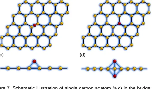
Adatoms
Interstitial atoms do not exist in graphene as in three-dimensional crystals, because of the high-energy requirement for the in-plane position [13]. However,
15
adatoms can exist in the third dimension in energetically favored bridge configuration without straining the crystal lattice, as shown in Figure 7 (a,c) [13]. Additional atoms can migrate not only over the graphene surface but also through-the-lattice and form metastable dumbbell configuration Figure 7 (b,d), which has higher barrier energy than bridge configuration. In addition to this, when two adatoms meet they form a dimer, which changes the curvature of graphene if agglomerated [13].
(a) (b)
(c) (d)
Figure 7. Schematic illustration of single carbon adatom (a,c) in the bridge; (b,d) in the dumbbell configuration.
Foreign (noncarbon) atoms also can exist as adatoms in graphene lattice as shown in Figure 8. Strong interactions between noncarbon atom and carbon lead to the formation of covalent bonds (chemisorption), while weaker interaction leads to physisorption due to van der Waals interactions[13]. The introduction of such defects changes the electronic properties of graphene. Another type of foreign adatoms is “inverse Stone-Wales defect”, which increases the reactivity of graphene sheet [13].
16
(a) (b)
Figure 8. Schematic illustration of noncarbon (metal-green) atom (a) on single vacancy (b) on double vacancy. Metal atoms use the third dimension.
Substitutional Impurities
Foreign atoms can replace one or few carbon atoms as substitutional impurities. Some impurities such as boron and nitrogen, which have radii close to Carbon's, behave as natural dopants since they have one electron less or more, respectively [13]. Electronicproperties can be changed by the introduction of transition metals impurities, located out of graphene plane, because of larger in size compared to a carbon atom. Covalently bonded impurities are expected to be stable and not to migrate throughout the lattice [13].
One-dimensional defects
One-dimensional or line defects can be observed in graphene lattice, caused by tilt boundaries separating domains with different orientations [13]. Usually, line defects are caused by simultaneous graphene nucleation at different points of metal substrates, leading to the formation of independent domains [13]. Different lattice orientations of graphene grains arise from the mismatch between graphene and metal [13]. Such defects have a significant influence on the
17
properties of materials, especially on two-dimensional material like graphene, which is extremely sensitive to defects. Atomic structure of grain boundaries and their sizes play important role in determining the properties of polycrystalline materials[13].
Edges defects
Generally, graphene edges prefer zigzag or armchair orientation because of minimum number of dangling bonds at the edges. Edge defects appear because of atom removal or reconstruction, caused by electron sputtering. Defective edges can consist of non-hexagonal rings such as five or six-membered rings. Saturation of dangling bonds with non-carbon atoms as hydrogen also causes structure disorder and increases defect numbers at the graphene edges[13].
The effect of defects on the properties
Defects are unavoidably introduced into graphene and TMDs during the synthesis, consequently presence of defects effects the mechanical and other properties of two-dimensional materials [33]. MD simulations showed that Young`s modulus of graphene linearly decreases with a concentration rise of SV defects, while elasticity modulus is less sensitive to Stone-Wales dislocations [27][41][44][45]. Also, MD simulations revealed that SVs have a higher influence on Young`s modulus of graphene compared to DVs because SV has more dangling bonds [41]. Also, the shape and location of defects play an import role in mechanical properties of graphene[41][45]. Reconstructed DV and SV defects show different effects on Young`s modulus, hence reconstruction of DV defect (without any dangling bonds) leads to the significant increase in modulus close to the pristine while reconstruction of SVs does not influence that much [41]. It was
18
suggested that by the saturation of dangling bonds of vacancy defects can improve the elastic properties of graphene [41].
The other interesting phenomena was observed by Lopez-Polin et al. They found out that introduction of defects could be an easy method for the increasing of the graphene`s Young`s modulus [46]. For this purpose, the suspended graphene sample was irradiated by a various dose of Ar+ [46]. As a
result, the highest 2D Young`s modulus of 550 N/m for the irradiated graphene sample with defect content of 0.2% was measured [46]. However, higher defect content leads to decrease in Young`s modulus of graphene as previously simulations showed. This unexpected influence of defects was explained by strong coupling between out-of-plane and in-plane fluctuations reflecting the anharmonicity [46].
19
CHAPTER 2
Materials and Methods
2.1 Graphene synthesis
Many researchers are still working on the synthesis of graphene and improvement of its quality. Some of the widely used synthesis methods are described below.
Exfoliation and cleavage
Graphene can be obtained from the bulk graphite by exfoliation or mechanical cleavage. The simplest way, used by Novoselov and Geim (2004), is to peel of graphene layers from highly oriented pyrolytic graphite (HOPG) mesa stuck on the photoresist by adhesive tape until monolayer or few layers are left on the photoresist. Although this method provides high-quality graphene, it is limited by low production [3][7][29].
20
For higher production chemical oxidation method was developed, however during the oxidation of graphite structural defects are introduced to graphene sheets[3]. The other drawbacks for chemical oxidation method are agglomeration and aggregation of graphene sheets, which compel to use stabilizers[3]. Also, high-quality graphene can be obtained by intercalation of small molecules between graphene sheets in graphite to prevent agglomeration [3].
Plasma-induced layer-by-layer thinning
Oxygen plasma
Oxygen plasma is one of the strongest conventionally used plasmas and it is a good oxidizing agent for carbon materials [47]. Oxygen plasma can etch graphite or graphene, hence it can be used for the top-down synthesis of graphene by layer-by-layer thinning of thick samples [47]. This method is suggested for obtaining graphene sheets with necessary thickness but it needs very precise control [47]. However, aggressive behavior of oxygen plasma leads to the generation of defects and destruction of the lattice structure, which changes properties of graphene [47].
Hydrogen plasma
Hydrogen plasma can be used for the preparation of graphene but the process needs an elevated temperature because hydrogen plasma is not efficient at ambient temperature [47]. Hydrogen plasma is weaker compared to oxygen plasma, therefore it is better for layer-by-layer thinning of graphene. Better control over the process makes hydrogen plasma an attractive method to obtain graphene with fewer defects compared to oxygen plasma [47]. The limitations of
21
this method are slow rate and necessity of adding heavier atoms like nitrogen (N) or argon (Ar), as well as the predominance of hydrogenation rather than etching of graphene layers [47].
Other plasmas
There are several other plasmas used for thinning of the graphene such as nitrogen, halogens, H2O2, air and noble gases. However, nitrogen plasma
functionalizes and dopes graphene, thus it is used less for etching. Noble gases, especially Ar, are also used for graphene etching but it takes too long compared to all other plasmas. The main drawback of all plasma assisted fabrication of graphene from the bulk sample is non-uniform etching of graphene sheets [47].
Chemical vapor deposition (CVD)
Thermal decomposition of SiC
Apart from exfoliation and cleavage methods, there are several more methods to prepare single or few-layer graphene (FLG), like epitaxial growth on SiC, graphene growth in CVD and plasma enhanced chemical vapor deposition (PECVD) [29]. In order to grow graphene epitaxially on SiC, SiC is heated to 1200˚C under ultrahigh vacuum (UHV) [5][10]. This method does not require any transfer process, what makes it attractive among other techniques [5]. The transfer of graphene grown on SiC to other substrates is possible, but conventional transfer method leads defects [29]. This method has some drawbacks as difficulties in controlling of thickness for large areas and various structural defects during the growth process, which affecting some electrical properties of it [3].
22
Plasma enhanced CVD growth of graphene
Plasma enhanced chemical vapor deposition (PECVD) is allowing to grow graphene flakes at lower temperature (650˚C) compared to conventional CVD systems. CH4 and H2 are used as precursors to synthesize graphene on various
substrates [3].
Chemical Vapor Deposition (CVD)
Among all methods, CVD growth is the most promising for large-scale growths [29]. First time it was used by Somani (2006) and it is successfully being used by researchers [3][5][48]. For first successful graphene synthesis in CVD system Ni foil was used, but nowadays other metal substrates such as Cu, Ir, Ru, Pt, Pd, Re, Rh, Co and some metal carbides are also used [5]. Amongst these metals, Cu is the most suitable, because of low cost and remarkably low carbon solubility [48]. Because of low C solubility in Cu, predominantly single-layer graphene is obtained under suitable condition [48]. After growth graphene must be transferred to other substrates depending on further processes and applications. Although the quality of CVD grown graphene is acceptable, during the wet transfer process some unwanted impurities and defects like cracks, vacancies, tears, folds, contamination can be introduced to the graphene [48].
Conventional wet transfer procedure roughly consists of following steps [48]: 1. Deposition of polymers (polymethyl methacrylate (PMMA),
polydimethylsiloxane (PDMS)) on graphene/Cu foil for temporary support.(Polymer/ Graphene/ Cu foil).
2. Cu etch.
3. Rinsing graphene/ polymer with deionized water (DI) water. 4. Fishing out graphene/ Cu foil onto a substrate (Si).
23 5. Complete polymer removal.
6. Rinse with acetone, IPA.
Many researchers are still working on optimization of transfer process in order to minimize the formation of defects. There are two methods used for metal etch: with and without polymer-support. Metal etch without supporting material was used by Hong group but it leads to the formation of ripples, cracks, tear on graphene, because of the high sensitivity of one atom thick graphene to even slight disturbance. Generally, polymer-supported Cu etching methods are preferred by researchers for high-quality and large graphene sample [29].
PDMS is the first polymer used as supporting material for graphene transfer, it has good properties like high durability, resistance to many solvents, low reactivity, moldability and low surface free energy [29]. The low adhesion force between graphene and PDMS provides an easy release of graphene from the supporting polymer, therefore allows to transfer graphene to substrate with higher surface energy [29]. Etch time for metal sandwiched between PDMS/graphene and the wafer is too long, what makes transfer made by the assist of PDMS weak [29].
PMMA is another conventionally used polymer for graphene transfer, which covalently bonds to graphene unlike PDMS having weak van der Waals force [29]. PMMA can be easily deposited on graphene/Cu in spin-coater and removed by acetone. Even so, it reduces the quality of monolayer graphene by introducing cracks and tears, because of ripples on graphene flake created during the growth and thus preventing graphene to make good contact with substrate[29]. The quality of graphene transferred by this method can be improved by coating graphene/ Cu by additional PMMA layer [29]. PMMA residues, caused by incomplete polymer removal by acetone, are other problem of using PMMA, which has an influence on physical and electrical properties of graphene. The post-annealing process was suggested as a solution for complete removal of PMMA residue from graphene surface [29]. Many other approaches like
24
electrochemical delamination and layer-by-layer graphene stacking were developed by use of PMMA [29].
Apart from PDMS and PMMA, other photoresists are being used as supporting polymer like Haas Shipley SA-1800. Graphene/ Cu is easily coated by drop cast method and annealed in a furnace, also it can be washed away by acetone. The simplicity of using photoresist makes it an attractive method to use. However, for full removal of polymer, it must be washed with acetone several times.
The polymer behaves like a backing layer, so the transfer process continues with the Cu etch step. For the Cu etch process several solutions are being used as etchants, like ammonium persulfate ((NH4)2S2O8), iron chloride (FeCl3), nitric
acid (HNO3), iron nitrate (Fe(NO3)3) and a mixture of hydrogen peroxide (H2O2)
and hydrochloric acid (HCl )[48]. Some of them are resulting in metal remain (Cu, Fe), that’s why the appropriate etchant selection is essential to avoid additional contamination. Another problem is tears, holes, and folds, mainly caused by water trapped between substrate and graphene. Complete removal of supporting polymer layer is also important to obtain clean and high-quality graphene samples. Generally, the polymer is washed away by acetone, another effective way of removing PMMA is annealing of the sample after acetone wash. All defects like residues, cracks, and tears can significantly, reduce the quality and affect some properties of graphene [48].
2.2 TMDs synthesis
All methods used for the synthesis of TMDs can be classified as top-down and bottom-up. Both of them have advantages over each other and disadvantages. Generally, top-down methods are preferred for the synthesis of high-quality TMD crystals which are mainly used for fundamental studies, while bottom-up methods are preferable for large-scale productions [19]. The production procedure of 2D
25
TMDs plays a significant role in their applications because the quality and properties of materials depend on the synthesis methods and control[22].
Exfoliation
The exfoliation approach used for the preparation of 2D materials is the top-down methods, which includes chemical, mechanical and solvent exfoliation [31]. Among these methods, mechanical exfoliation of the bulk crystal is the best way to obtain extremely clean samples of different thicknesses [31]. Consequently, 2D TMD crystals obtained by mechanical exfoliation are the mostly used for device demonstrations and fundamental research[31]. By the mechanical exfoliation of bulk TMDs, samples with the thicknesses varying down to single layer can be prepared, however, flakes are limited by small sizes [31].
The chemical and electrochemical exfoliation approach is preferred for solution-based and printable electronics with a relatively large quantity production [19][31][49]. The lithium intercalation is the one example of this method, where lithium reactants such as n-butyllithium in hexane are used for the intercalation of TMD layer bonded by weak van der Waals interaction [23]. In addition, bulk TMDs can electrochemically intercalated but its mechanism is not well studied yet[23]. Other ions like alkali metals can be alternative candidates for the intercalation of TMDs [23].The yield of single layer TMDs prepared by this method is high enough [23]. Contaminations, doping, defects and poor control over the thickness and size are limitations of this method[19][31]. Also, this method is time-consuming, sensitive to the environment, compatible only with some solvents and might need a post-treatment for reconstruction of lattice structure which can be modified during the exfoliation procedure [19][50].
The third exfoliation method is solvent-based, which allows producing large quantities. In contrast with chemical exfoliation, common solvents can be used for the preparation of few- and monolayers of TMDs [50]. In addition, it is
26
insensitive to water and air and can be a good approach for the synthesis of hybrid films[50]. Contaminations and poor control over the thickness and size are the drawbacks of this approach [31].
CVD growth
Since the number layers and the size ( area) of 2D materials significantly affect the performance and properties of nanosheets/flakes, development of a new strategy to overcome problems of conventional exfoliation methods was necessary. The CVD growth of 2D materials is the very promising bottom-up approach. This approach can be characterized as a very reliable method with precise thickness control, which allows growing large-sized graphene and TMD nanosheets [31]. Generally, for the growth of TMD crystals chemical vapor is generated from the solid source by its evaporation and vapor is carried by inert gases like Argon (Ar) or Hydrogen (H2) [31].
There are several reported CVD growth processes, in which different precursors are used. So MoS2 is grown by sulfurization of Mo film deposited on
SiO2/Si substrate by sulfur vapors [16][19]. It is an easy and fast way for growing
MoS2 on an insulating substrate, where the thickness and lateral dimensions
depend on the deposited Mo film [19]. The lack of uniformity ( single and few-layer MoS2), metallic property and low on/off rate possibly caused by metal
remains are the limitations [16][19]. Another variation of the same method with a relatively high uniformity is a synthesis of the vertically aligned MoS2, which can
be grown on the various substrates including glassy carbon, quartz and oxidized silicon by the rapid sulfuration [19]. In this method sulfur is the limiting reactant [19]. For the large area, MoS2 growth metal film can be replaced by the MoO3
layer. As a result film with high on/off ration current can be obtained. Similarly, WS2 films can be synthesized by this strategy [19]
27
The Atomic Layer Deposition( ALD) offers a high thickness (layer number) control and good uniformity for the TMDs( WS2) growth [19]. The number of WS2
layers can be controlled by the cycle number of precursors WO3 [19]. The MoS2
also can be produced by ALD, however, resulting material can suffer from the low uniformity, small crystal grains and polycrystallinity [19]. It was suggested to overcome this issue by the peeling of the top MoS2 layer with a PMMA, but it
might generate defects and damage the nanosheet [19].
Also, 2D TMDs with a quality and electrical properties comparable with a exfoliated TMDS can be obtained from the thermal decomposition of thiolsalts like (NH4)MoS4 (ammonium thiomolybdate) [16][19]. However, this method has
some drawbacks like polycrystallinity, long and complicated procedure, including technical difficulties in the deposition of uniform (NH4)MoS4 film [19].
The direct reaction of vapor phases of metal oxides like MoO3 or WS2 and
S powders results in a single-crystalline MoS2 and WS2 on different substrates
[16][19]. In addition, aromatic and inorganic seed molecules like reduced graphene oxide (r-GO) or hafnia (HfO2) can be used for promoting the growth
[16][19]. The MoS2 powder transported to the insulating substrate by the physical
vapor allows producing monolayer MoS2 with good optical properties [19].
It worth noting that heterostructures/ alloys of TMDs became critical for the band-gap tuning. This alloys can be produced by both top-down and bottom-up approaches [19].
2.3 Characterization methods
Generally, several characterization methods are used for imaging 2D materials such as optical microscopy, scanning electron microscopy (SEM), atomic force microscopy (AFM), Raman spectroscopy, Transmission electron microscopy (TEM) [3]. Generally, a combination of few techniques is used for characterization of graphene and 2D TMDs.
28
Optical imaging
Optical microscopy is the cheapest and easiest nondestructive methods for imaging samples. However, for graphene samples, it is very important to choose suitable substrate for better contrast. Silicon covered with dielectric SiO2 and
Si3N4 is the most commonly used substrate, because of enhanced contrast[3].
The wavelength of incident light is another key factor for enhancing the contrast[3]. As a result, suitable selection of incident light and substrate makes it possible to image graphene flakes in optical microscopy. TMDs can be imaged by the optical microscopy on Si substrate.
Transmission Electron Microscopy (TEM)
Generally, TEM is used for imaging samples with atomic resolution. In TEM electron beam is transmitted through the suspended thin sample and collected in detector [3]. This method makes it possible to obtain the atomic structure of material only at low operating voltages, since a high voltage, like 80 eV, is sufficient to introduce defects and damage monolayer graphene sheets [3][11].
Besides, TEM gives information about the crystallinity of material, thus amorphous structures and contamination can be easily distinguished [3]. Meyer et al. could directly image all individual carbon atoms of graphene and theoretically predicted defects like Stone-Wales, vacancies and line defects[11].
29
Scanning Electron Microscopy (SEM)
Another characterization technique is SEM (ESEM1), which gives an opportunity
to obtain more detailed images of samples. Details like folds, tears, wrinkles, and contamination can be seen in high-resolution SEM images [51][52]. SEM is widely used for imaging suspended graphene and TMDs, and also graphene or TMDs on substrates like Si, copper (Cu) foil, Si3N4/Si or SiO2/Si [53][54].
Raman spectroscopy
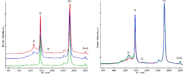
Raman spectroscopy is the nondestructive and simple method, which allows obtaining valuable information about the vibrations of crystal lattices and accurately determine the layer number of graphene and TMDs[55]. In Raman, an incident light (laser) sent to the crystal emit or absorb phonons and scattered in materials [20]. Hence, Stokes (photon loss) and Anti-stokes (photon gains) are detected and analyzed [20].In Raman spectroscopy carbon allotropes have distinctive peaks around 1350cm-,1600 cm- and 2700 cm- known as D,G and 2D
(G`), respectively [55][56]. These peaks provide valuable information about defects, layer number, doping concentration, the effect of strain and temperature [3][57][58]. D-band is related to defects and G-band is a result of in-plane vibration of sp2 carbon atoms while stacking orders are denoted as 2D (G`)-band
[55]. The G-band is a doubly degenerated E2g phonon mode at the Brillouin zone
center and 2D-band is associated to the inter-valley double-resonance Raman scattering [3][56][57][58]. D band arise because of disorders and defects in the structure, fluctuation and charge puddles, therefore D band absent in pristine graphene[3].
As it was mentioned above, Raman spectroscopy allows to accurately measure the number of graphene layers. Single-layer graphene can be easily
30
distinguished from graphite, by comparison of G and 2D (G`) band peaks. Monolayer graphene has a very sharp 2D band and low G-band intensity, whereas G-band intensity rises almost linearly with the increase of layer number [55][58]. Also, the 2D band splits to few components for few-layer graphene, broadens and shows a blue shift[3]. The Raman spectroscopy and PL spectroscopy can be used for determining the layer number, doping and strain of TMDs [21].
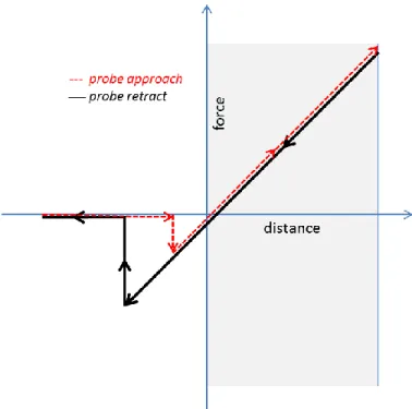
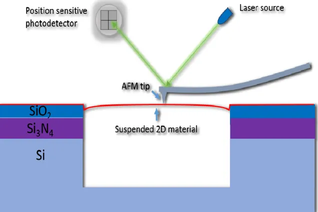
Atomic Force Microscopy (AFM)
Generally, the thickness and topography of graphene and TMDs are directly measured by AFM, which works on the principle of changes in attraction and repulsion forces between material and tip caused by van der Waals interactions. When the tip comes into contact with a sample the force goes to zero (straight line) and the tip is attracted, resulting in a dip in the force-distance curve as can be seen from the Figure 9 then it is repulsed. The position-sensitive photodetector measures the deflection of the cantilever to the extension of the piezoelectric scanner and force-distance curve like in Figure 9 is obtained. The displacement can be calculated from the Equation (4) given below:
z
piezo= Ƞ
piezo+ Δz
material (4)where Ƞ piezo is a deflection of a tip, z piezo is the location of piezo and the Δzmaterial
is the deflection of the material. However, AFM has an instrumental offset of 5 Å, which is higher than the thickness of single layer graphene leads to incorrect measurements [55]. Apart from these, because of high sensitivity to small forces caused by deformation of materials, AFM can be used for mechanical characterization of 2D materials [3]. Other modes of AFM allow determining magnetic, frictional, electrical and elastic properties of samples [3][34].
31
Figure 9. Schematic illustration of Force-distance curve.
2.4 Measurement of Young`s modulus of 2D materials
There are several methods used for measurement of Young`s modulus of graphene, as nanoindentation and Raman-based. While the nanoindentation is a robust method for measuring the elastic properties of both graphene and TMDs. These two methods are described below.
Raman-based measurements
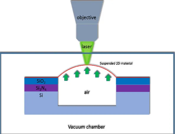
Raman is the non-destructive method used for investigating intrinsic properties of materials, which also can be used for measurement of the Modulus of Elasticity [59]. Owing to impermeability of pristine graphene to all gases, Young`s modulus of defect-free graphene can be estimated by Raman with a simple setup illustrated in Figure 10 [59]. As it can be seen from the Figure 10, graphene is
32
transferred onto Si/SiO2 substrate with a blind hole, what allows to confine an air
in well. The prepared system is placed in a vacuum chamber for manipulation of the pressure applied to the suspended graphene by changing the vacuum value. When the vacuum chamber is evacuated chamber pressure drops, graphene bulges upward due to the pressure difference caused by air confined in Si well under graphene [59]. As the vacuum increases the biaxial strain increases, and thus graphene begins to deform [59].
Because of the high sensitivity of Raman spectroscopy to mechanical deformations, accurate measurement of strain resulting the deformation is possible[59]. Researchers have shown that G and 2D bands of graphene are showing red-shift and each of them splits into two because of deformation [59]. Measured strain cannot be used itself, but it must be compared with the values calculated in finite element methods [59].
.
Figure 10. Schematic illustration of the experimental setup used for measurement of Young`s modulus by Raman.