The Operation of a Novel Hot Electron
Vertical Cavity Surface Emitting Laser
N. Balkan, A. O'Brien, A. Boland Thorns, R. Potter, N. Poolton, M. Adams, J. Masum,
tA. Bek, tA. SerpengUzel, tA. Aydinh, and J. Roberts
Essex University, Department of Physics, Colchester, Essex, C04
3SQ,U.K.
1• Bilkent University, Department of Physics, Bilkent, Ankara 06533,
Turkey.
lSheffield University, Department of Electronic and Engineering, Sheffield, U.K.
ABSTRACT
The hot Electron Light Emission and Lasing in Semiconductor Heterostructure devices (HELLISH-i) is novel surface emitter consisting of a GaAs quantum well (QW), within the depletion region, on the n side of GaiA1As p-n
junction. It utilises hot electron transport parallel to the layers and injection of hot electron hole pairs into the quantum well
through a combination of mechanisms including tunnelling, thermionic emission and diffusion of lucky' carriers. Super
Radiant HELLISH-i is an advanced structure incorporating a lower distributed Bragg reflector (DBR). Combined with the finite reflectivity of the upper semiconductor-air interface reflectivity it defines a quasi-resonant cavity enabling emission output from the top surface with a higher spectral purity. The output power has increased by two orders of magnitude and
reduced the full width at half maximum (FWHM) to 2Onm. An upper DBR added to the structure defines HELLISH-VCSEL which is currently the first operational hot electron surface emitting laser and lases at room temperature with a l.5nm FWHM. In this work we demonstrate and compare the operation of UB-HELLISH-l and HELLISH-VCSEL using
experimental and theoretical reflectivity spectra over an extensive temperature range.
Keywords: Hot electron laser, surface emitting device, longitudinal transport, Vertical Cavity Surface Emitting Laser(VCSEL).
1. INTRODUCTION
The Vertical Cavity Surface Emitting Laser (VCSEL) has become one of the most important devices in recent years. It was first realised in 1979 but did not come to fruition until growth systems such as Molecular Beam Epitaxy
(MBE) and Metal Organic Vapour Phase Epitaxy (MOVPE) advanced sufficiently to cope with such stringent and precise
requirements. ( for a review see 1). Since then the interest and research in this area has avalanched and the VCSEL has
improved enormously in terms of power output and efficiency. In fact VCSELs with efficiencies up to 55%andpowers of
around 5mW single mode from GaAs quantum wells have been reported2. These devices can now rival conventional semiconductor lasers and are available commercially, VCSEL technology has also been extending into the visible
wavelength range.
There have also been many advances in the direction of novel, light emitting devices based on longitudinal
transport. One type of longitudinal transport light emitting device is known as CHINT3. In this structure hot electrons are transferred in real space between two separately conducting channels. If the second channel is a complementary layer then it has been shown that light emission occurs which has an intrinsic logic function with respect to the electrical inputs.
HELLISH (Hot Electron Light Emission and Lasing in Semiconductor Heterostructure) is another novel
longitudinal transport device. This has been researched extensively resulting in two main types of devices; HELLISH-i and 2.46 HELLISH-i consists of a 130A GaAs SQW situated on the n-side of an AlGaAs p-n junction within the depletionregion. Light emission is from the device surface, independent of the applied electric field and therefore exhibits an XOR
function with respect to the applied voltage. HELLISH-2 has a similar material system but is a more complex structure as it includes an inversion layer and a multiple QW (MQW) structure with QW's of varying well widths. This has been shown to produce multi-wavelength operation and logic tasks which are discussed in detail elsewhere78.
HELLISH-i has been adapted and converted from an LED to a super radiant structure by the addition of a DBR
lost Iioio
lie device Ites and
hsiratc is reflected hacL tliioiih the device. The GaAs-au ntei lace has
reflectivity olapprsiliiitcIv
()
dueto iliscoiitiiiuities in the refractive iiid'x. and forms a j irtial or quasi-cavity. Altliouh there
arcniaii losses 11(1111 tIle
tipper surface (7IY ) the device is still able to maintain a high enough photon (lensitv to initiate
stiiiiiilatcd eiriissioii 'Flierelore it is able to operate as a super radiant structurebased on stirniihited eiiiissioii rather than
emission as ii the niginal device.
Recentl\ a \'('SFl device has been realised by iiicorpoiitinZ an upper and lower l)UR to the original structure. In this case the original IIFLLISII structure defines the cavity and this device is able to lase at room temperature. lo date this is the first demonstration of a hot electron based \!('SEI at room tertiperattire.
2. RESULTS
ANI)
DISCUSSIONS
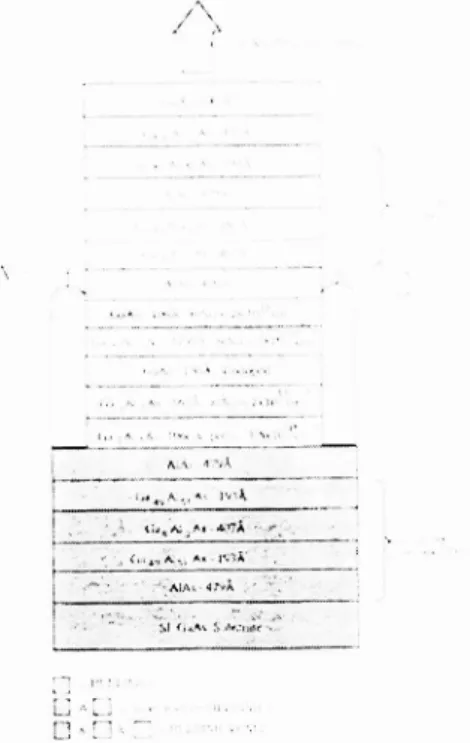
Al three waters crc grown by MOVPE on semi—insulating GaAs substrates and thestructures aieitiven by
I As shown in the kes. HELLISI I-I
forms the cavityof I1ELLISH-VCSLL; and SuperRadiant HELLISI I consistsof the lower and active region.
The lowerDI3R has 27 periods of AIGaAs layers withvarying Al concentration and
provides a reflectivity better than99(4• Theupper DBR is iiiuch thillner andonly has 17 periods which
allo
s an outputfioni thetopsurilice inthe
tori
of
lasing. The QW is centralisedwithinthe
active region inorder tocoincide with an anti— lode of the confined optical field therefore increasingefficiencyby maximlsiflgpair] with each iou nd tripthrough the cavity.For all threestructures the devices investigated were simple bars and Hall barsfabricated over a
l(R)prii to .iiitu
range. Au/( ic/Ni contacts were evaporated directl\ onto the top layer then diffused through all avers for the devices without the upper DBR. With I IELLISI I-VCSEL the upper I)HR had to he selectively etched in order to evaporate contacts directly
onto the n region after which ther were diffused through the active layers. (' ontacts were tested for each of device avers
uid weie ohrriic oven' 70K<i'<300K. which is the usual operating range.
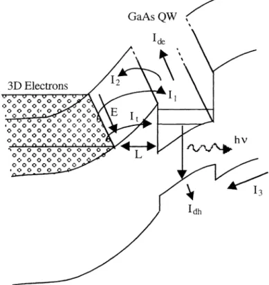
The operation of the device is based on the heating of electrons and holes in their respective channels in the
iao 7Al() p- junction by the application of longitudinal electric fields4. Due to their lower elective mass the electrons heat up more readilr than the holes and occupy higher energy levels. Non equthihnuni electrons mjection into the quantliiii well ma occur through the following injection mechanisms: The occupation of the higher -I) states in the n-las ci is in
4A (...,A.,,
- ' 'AIM - 4A - S
effect identical to the lowering of the built-in potential by the application of a forward bias in a conventional p-n junction
device. Therefore, effective lowering of the potential barrier should enhance both the tunnelling and the thermionic
injection of hot electrons into the quantum well as depicted in figure 2andas described in (4-6). The dominant mechanism
at low fields is expected to be the tunnelling process. The accumulation of excess negative charge in the depletion region induces a self modulation of the junction. The n-side potential barrier increases, while the p-side depletion region and
potential barners decrease enhancing hot hole diffusion into the QW. Another mechanism that may contribute to the overall injection, particularly at intermediate and higher electric fields , isassociated with the well-known 'lucky drift' model9. The hot carriers drifting towards the appropriate contact in their respective channels suffer collisions with phonons which lead to relaxation of momentum and/or energy. In the 'lucky drift' model the carrier velocity is determined by momentum-relaxing collisions without there being in the same period any significant energy relaxation. Whilst this lucky drift is occurring in the
transverse direction, the carriers can also diffuse in the orthogonal direction towards the opposite side of the junction (i.e.
hot electrons go towards the p-side and hot holes towards the n-side). Thus these carriers can gain sufficient energy from the
field to be captured by the quantum well. Since the holes have to gain considerably more energy than the electrons (as a
consequence of the position of the quantum well with respect to the junction), it follows that the region of the device where the recombination of carriers in the well is maximised is offset towards the cathode. Infra-red photographs of the near-field emission indicate that much of the radiation is generated near the cathode, in agreement with this qualitative theory. More quantitative estimates of the device performance based on this model will be the subject of future work.
Radiative recombination takes place in the QW. Because the operation of the device is based purely on electric
field heating of carriers, the resultant light emission is independent of the polarity of applied bias.
Figure 2: The carrier dynamics involved with HELLISH-i operation. E is applied longitudinal electrical field, Ij and It are injection of excess electrons into the wefl by thermionic emission and tunnelling respectively. '2 is the total (thermionic emission and tunnelling) reverse current from the well. Ide and idh are electron and hole drift currents, respectively, and 13 is hot hole diffusion into the quantum well.
GaAs QW
'de
3D Electrons
.-.c. j c'
'-'0000000
0000000 0
0 0 0 C. 0 v
0 r
0 C0 0 0
-,. 0
0 0 0 C' 0
0 0 0 0 0 0 C 0 0
o 0 0 0 0 0 0 0 0 0
0 00000000(
0000000000
.
(. ? .. ..
r .
0 0 0 0 0 0 0 0 C
0 000 00000.
0 0 0 0 0 0 0
-0000
0 0 0 0 0
'dh
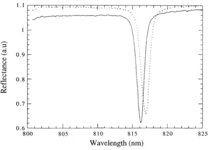
With the two advanced structures the operating principles are exactly the same and only difference is that the DBR reflectivity spectra determines the quantity of light emission from the sample surface. It is not just the intrinsic hot electron effects that are responsible for the emission spectrum, but the combination of HELLISH EL spectra (gain spectra) and DBR
reflectivity spectra. The room temperature reflectivity spectra for Super Radiant or Ultra Bright (UB) HELLISH) is given by Figure 3. In the UB device all emission normally lost through the substrate in HELLISH is reflected back through the device via the lower DBR so increasing the photon density. Although the reflectivity spectra does limit the light emission, there is no distinctive cavity resonance, so a large degree of stimulated emission will be emitted. In the case of HELLISH-VCSEL, however, there is a definite cavity and resonance wavelength at 816 nm as also shown in figure 3. Therefore the majority of photons are confined to the cavity, losses are low so lasing is possible on a single longitudinal mode at the
resonant wavelength. 90 80 70 60 50 40 30 20 10
Figure 3: (a) The reflectivity spectra for HELLISH-VCSEL and (b) Super Radiant HELLISH at room temperature.
This description is summarised by Figure 4 which shows the electroluminescence (EL) spectra for each device.
These experiments were performed by applying electrical pulses with a duration of 3Rs and duty cycle less than 1% parallel
to the device layers. By comparing the spectra of all devices it is possible to see the development of a HELLISH LED to
VCSEL.
HELLISH-I has a broad EL spectrum with peaks at around 1. 46 eV and I .54 eV. The light emission extends over a 1 10 nm range, from 780-890 nm, and has a FWHM of 70 nm. With UB-HELLISH the EL intensity has increased by two
orders of magnitude. Note that the HELLISH EL spectrum has to be increased forty times to fit onto the same graph. UB-HELLISH spectrum has a main peak at 820 nm (1.52 eV) and a reduced FWHM of 20 nm as defined by the quasi-cavity resonance of reflectivity spectrum in 3(a). The high energy tail of the HELLISH -1 is also modulated by the reflectivity spectrum to give the small hihg energy peaks in the UB spectrum. With HELLISH-VCSEL the EL spectrum has a peak at
816 nm (1.52 eV) with the FWHM is reduced to 1 .5 nm as defined by the cavity resonance in figure 3(b). For both theUB and VCSEL structures the resonant wavelength was observed to shift by nmas a function of position on the wafer. This
variation is accounted for by the non-uniformities in DBR layer thickness commonly obtained with MOVPE grown
material'2
> Q 100b
0 600j
650 700 750 800 850 Wavelength(nm) 0 900 950 1000 650 700 750 800 850 900 950 1000 1050 lit wavelength (nm)rj)
0
0
H-VCSELx5UB-HELLISH
— — - HELLISHx4OI
0.7 0.6 -:. -0.5 -: -600 650 700 750 800 850 900 950 Wavelength(nm)
Figure 4: A comparison of EL spectra for HELLISH- 1 ,UB-HELLISHand HELLISH-VCSEL at room temperature.
If the reflectivity spectrum of a HELLISH-VCSEL 3x1 mm device is considered ,shownin Figure 5, then it can be seen that the resonance wavelength shifts by at least 1 nm across the length of the device. Therefore this coupled with the 1 nm resolution of our monochromator results in a resonant frequency width of 1 .5 nm and hence explain why the observed
FWHM of VCSEL spectra is 1.5 nm. This could be improved by reducing the non-uniformities during growth and
optimising device design for example by reducing the size of the surface area.
1.1 0.9 0.8 0.7 0.6 800 825 Wavelength(nm)
Figure 5: Reflectivity spectra from the two end points of a 3x1 mm HELLISHVCSEL simple bar at room
Altlioiih this
structure is tar from optiinised a whole ran'e 01 device tiptiratiotis have been tested .iinl all ha\ C emitted light\vmtll lie expected characteristics. In figure (i we sl'u an inira-red photoraph of the siii face eniisslon liomimtOni LILI INtl \'CSH at E=7(H) V/cm. The efketmve exposure tune is of the order of one second. 1)espiie the huge sue 0) the device the intensity is remarkably unitrm. In devices with comparable lengths . however, the emission is lot ,i1wa s uniform htit tends to concentrate nearer to the cathode Currently the smallest operational device is a I (X)x75 pm 111.1.11511 \ (d " hiich ieluires ((V tim achieve an applied electrical field of I kV/cni. 11 a l(hpm structure can be realised then this
ill ouls require IV to obtain an electric field if I KV/cni which is comparable to conventional V('SEI.s.
P igureIi: I nfra—red photograph of the surface emission froma 3.5 mm HELd .ISH—VCSEI at F=7(.8)V/cni
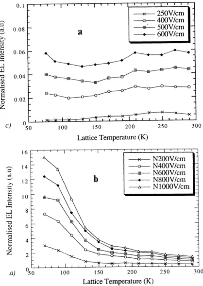
In I inure 7(a and (hI we show the temperature dependence of the emitted light intensity for L—IELLISI-I- I and HEI LISH- VCSEL. It is evident front the figure that the VCSEL efficiency has a much stronger temperature (lcpcndence than the simple device. It is reduced by about a factor of 7.5 when the teniperature is increased from 1=77 K to rooni temperature. This reduction can be partl due to the disparity in the temperature dependencies of the cavity resonance wavelength and GaAs QW hand gap. and hence the gain peak. This is illustrated in figure 8 where the calculaled band gap and the cavity resonance wavelength are plotted against temperature. In figure 8 we also plot the experimental results of temperature dependence of the resonance mode of HELLISH-VCSEI, and gain peak (EL peak) of the HELLISH-I device. Both the theoretical and the experimental result show that the difference between the resonance mode and the gain peak increases with teniperature giving rise to reduced efficiency at high temperatures as observed.
(ID (ID
0
z
(ID LL'0
(ID0
z
Figure 7: Temperature dependence of the emitted light as a function of temperature. (a) HELLISH-i device and
(b)HELLISH-VCSEL
In order to compare these structures with conventional devices it is necessary to consider the output power of a 3x1
mm device for each structure at room temperature, as given by Figure 9. HELLISH-i and UB-HELLISH were analysed up to an electrical field of 1.2 KV/cm and gave 2. 1 mW and 4.7 mW respectively. HELLISH-VCSEL was also investigated for thermal stability and tested up to 2.7 KV/cm. Increasing the electrical field to I .8 KV/cm gave an output power of 5.5mW
but after this point the device began to heat and the power saturated. In all structures emitted power was independent of the
applied electrical field. HELLISH-VCSEL is currently an unoptimised structure and produces 5.5mWsingle longitudinal
mode emission but has many transverse modes due to the large dimensions of the devices investigated The efficiency is estimated to be around I %,however,by optimising device design, growth and by fabricating
smaller devices this should be improved.
0.1 0.08 0.06 0.04 0.02 ———-— 1 _____________________________ 250V/cm
—c—
400V/cm500V/cm
-a
•
600V/cm 0 Cj 50 100 150 200 LatticeTemperature (K) 250 300 16 14 12 10 8 6a)
050 100 150 200 250 300 Lattice Temperature (K)E
0
0)0
0.95 0.90 a 0.85 0.80 Bandgap Resonance Mode 0.75 100 200 300 400 Temperature (K) 7 6 86() .. 05(1 - A a E 840 a b-
a 030 a:
a 820 £ a A a __•_ -.—
810 a....— , 800 50 00 • 150 200 250 300 350 LatticeTemperature (K)Figure 8: (a) Calculated temperature dependence of the band gap (upper line) and the cavity resonance wavelength (b) Experimental temperature dependence of the HELLISH EL (gain) peak wavelength (triangles),and HELLISH -VCSEL
Emission peak (as modulated by the cavity resonance)
5 4 3 2 0 0 500 1000 1500 2000 2500
AppliedElectric Field (V/cm)
3000
3. CONCLUSIONS
The operation of a novel hot electron light emitter has been demonstrated. With the introduction of a lower DBR the device is shown to emit ultra bright light with enhanced spectral purity. When the device is placed into a vertical resonant cavity consisting of a couple of BDR mirrors, it lases with an output power of 5.5mWin single longitudinal
mode. The device is very simple to fabricate in 2-D arrays with only two diffused-in point contacts required. The operation of the device is determined by the applied electric field and therefore, light emission is independent of the polarity of bias voltage.
4. ACKNOWLEDGEMENTS
We are grateful to EPSRC for funding the project (GR1L35034). N. B is grateful to TUBITAK, Turkey for TOKTEN
consultancy at Bilkent University.
REFERENCES
1 . T.E. Sale,' Vertical Cavity Surface Emitting Lasers, Research Studies Press Ltd. Taunton, Somerset, England
(1995)
2. C. Jung, R.Jager, M. Grabherr, P.Schitzer, R. Michalzik, B. Weigi, S. Muller, and K. Ebeling 4.8 mW single mode oxide confined top surface emitting vertical -cavity lares diodes" Electronics Lett. 33, pp 1790-1791 (1997)
3. S. Luryi, 'Light emitting devices based on the real space transfer of hot electrons', Appl. Phys. Lett. 58,
ppl727-l729 (1991)
4. A. Straw, N. Balkan, A. O'Brien, A. da Cunha and R.Gupta and M. Arikan,'Hot Electron Light Emission and Lasing Semiconductor Heterostructures Type 1', Superlattice and Microstructures 18 pp.33 (1995)
5. N. Balkan, A. da Cunha, A. O'Brien, A. Teke, R.Gupta, A. Straw and M. Arikan, 'Hot Electron Light Emitting Semiconductor Heterostructure Devices (HELLISH) Type 1&2', Proc. of HCIS Int. Conf 'Hot Caniers in Semiconductors' ed. K. Hess, J.P.Leburton,U. Ravaioli, Plenum Press, pp6O3-6O9 (1996)
6. A. O'Brien, N. Balkan and J. Roberts,'Ultra Bright Surface Emission From a Distributed Bragg Reflector Hot
Electron Light Emitter', Applied Physics Letters 70(3) pp366-368 (1997)
7. N. Balkan, A. Teke, R. Gupta, A. Straw, J. H, Wolter and W. van Vleuten, 'Tunable wavelength hot electron light
emitter', Appl. Phys. Lett. 67 (7), pp. 935-937 (1995)
8. A. Teke, R. Gupta, N. Balkan, W van der Vleuten and J. H. Wolter, 'A tunable hot-electron light emitter', Semicond. Sci. Technol. 12, pp. 3 14-320 (1997)