FOURIER TRANSFORM PLASMON
RESONANCE SPECTROMETER
A THESIS SUBMITTED TO
THE GRADUATE SCHOOL OF ENGINEERING AND SCIENCE OF BILKENT UNIVERSITY
IN PARTIAL FULFILLMENT OF THE REQUIREMENTS FOR THE DEGREE OF
MASTER OF SCIENCE IN
MATERIAL SCIENCE AND NANOTECHNOLOGY
By
Doolos Aibek uulu
January 2017
ii
FOURIER TRANSFORM PLASMON RESONACE SPECTROMETER By Doolos Aibek uulu
January 2017
We certify that we have read this thesis and that in our opinion it is fully adequate, in scope and in quality, as a thesis for the degree of Master of Science.
___________________________________________ Coşkun Kocabaş (Advisor)
___________________________________________ Aykutlu Dana
___________________________________________ Alpan Bek
Approved for the Graduate School of Engineering and Science:
___________________________________________ Ezhan Karaşan
iii
ABSTRACT
FOURIER TRANSFORM PLASMON RESONANCE
SPECTROMETER
Doolos Aibek uulu
M.S in Material Science and Nanotechnology Advisor: Coşkun Kocabaş
January, 2017
Nanophotonics is an emerging field of research aiming to control interaction of light with matter in nanometer scale. Electrons localized on metallic nanoparticles generate localized plasmon oscillations with interesting optical properties that can be used for various sensing applications. Spectroscopic sensing using plasmonic particles could provide more detailed information, however it requires bulky spectrometers which limits its applications. In this thesis, a nanometer scale Fourier Transform Plasmon Resonance (FTPR) spectrometer is presented. FTPR spectrometer consists of a nanometer slit-grove or slit-ridge plasmon interferometer with varying optical path. The inherent coherence of the surface plasmons propagating through the sub-wavelength holes yield high contrast spatial interference pattern. FTPR spectrometer converts this spatial interference pattern in to spectroscopic information using Fast Fourier Transform (FFT) algorithm. In our design, there is no need for a bulky dispersive spectrometer or dispersive optical elements. We anticipate that high sensitivity of surface plasmons together with spectroscopic information and nanometer dimensions provides new avenues for plasmonic sensors.
iv
ÖZET
FOURİER TRANSFORM PLAZMON REZONANS
SPEKTROMETRESİ
Doolos Aibek uulu
Malzeme Bilimleri ve Nanoteknoloji, Yüksek Lisans Advisor: Coşkun Kocabaş
Ocak, 2017
Nanofotonik bilimi ışık ile nanometre boyutundaki cisimin etkileşmesini kontrol etmeyi amaçlayan alan olarak bilinmektedir. Nanoparçacıkların üzerindeki elektronların plazmon osilasyon üretmesi ile birlikte ilginç optik özellikleri bir çok sensör uygulamalarında kullanılır. Plazmonik parçacıları kullanarak ayrıntılı detaylı spektroskopik bilgi edilebilir, ama spektrometrelerin geniş hacimli olması plazmon uygulamalarını sınırlıyor. Bu tezde, Fourier Transform Plazmon Rezonans (FTPR) Spektrometresi geliştirilmiştir. FTPR spectrometre nanometreler büyüklüğünde kesik-oyuk veya kesik-çıkıntı şeklinde ışık yolu değişebilen plazmon interferometre içerir. Değişebilen ışık yolu dolayısıyla, dalga boyundan küçük delikten geçen ışık yüksek kontrastta girişim örüntüsü oluşturmaktadır. Biz ışığın spektroskopik bilgisini elde etmek için plazmonik interferometre kullandık. Bizim spektrometremiz boyutsal girişim örüntüsünü Hızlı Fourier Transform algoritması kullanarak spektroskopik bilgiye dönüştürmektedir. Bizim tasarımımızda, hacimli dağınımlı spektrometreye ya da dağınımlı optik parçalara ihtiyaç duyulmamaktadır. FTPR spectrometresi yüzey plasmonların hassasiyetine ek olarak spektroskopik bilgiyi kullanarak nanometre boyutunda yeni bir sensor olacağını öneriyoruz.
v
Acknowledgement
First, I would like to express my most sincere gratitude and appreciation to my advisor Prof. Coşkun Kocabaş. His guidance and support have always motivated me throughout the time of my research and study. Without his guidance and support this thesis would not have been possible.
I would also present my gratitude to Prof. Aykutlu Dana and Alpan Bek for their judgments and helpful critics as the thesis committee.
Especially, I am thankful to Dr. Nurbek Kakenov and Dr. Osman Balci. Without their help, none of the Fourier Transform Plasmon Resonance spectrometer measurements would have been possible.
I would like to thank Kocabaş Research Group, both present and former members for providing me wonderful atmosphere during the course of the years. Namely, I thank Dr. Evgenia Kovalska, Dr. Eda Goldenberg, Pınar Köç, Burkay Uzlu, Zeinab Eftekhari.
Above all, I am grateful to Timur Ashirov, Eliza Sopubekova and Begimai Adilbekova for their support and guidance throughout during my two years that I spent at Bilkent University.
I am also thankful to the faculty and staff of UNAM for providing me delightful atmosphere throughout my study.
I dedicate this dissertation to my family. I am thankful to my father Aibek Turdakunov, my mother Gulmira Abdyrazakova, my sisters Nurperi Alakunova, Aigul Alakunova and Malika Alakunova for their love, care, and patience.
vi
vii
Contents
1 Introduction 1
1.1 Organization of thesis ... 4
2 Surface Plasmon Polaritons 6 2.1 Optical properties of noble metals ... 6
2.2 Drude-Sommerfeld theory ... 7
2.3 Interband transitions ... 9
2.4 Surface plasmon polaritons at plane interface ... 10
2.5 Properties of surface plasmon polaritons ... 12
2.6 Excitation of surface plasmon polaritons ... 14
2.7 Application of surface plasmon resonance ... 20
3 Plasmonic Interferometers 22 3.1 Extraordinary transmission through subwavelength apertures ... 22
3.2 Plasmon interferometer ... 24
3.3 Application of extraordinary transmission ... 27
4 Focused Ion Beam (FIB) and Electron Beam Induced Deposition (EBID) 28 4.1 Focused Ion Beam (FIB) ... 28
4.2 Electron induced beam deposition ... 33
4.3 Focused Ion Beam applications ... 35
viii
5.1 Fabrication ... 38
5.2 Experimental setup ... 40
5.3 Results ... 42
5.4 Optimum thickness of platinum ridge for high contrast interference fringes 44 5.5 Plasmonic decay ... 46
6 Fourier Transform Plasmon Resonance (FTPR) spectrometer 48 6.1 Fourier Transform Infrared spectrometer ... 48
6.2 Static Fourier Transform Spectroscopy ... 52
6.3 Wavelength of surface plasmon polaritons... 55
6.4 Fourier Transform Plasmon Resonance spectrometer ... 60
7 Discussion and conclusion 69 7.1 Advantages of Static Fourier Transform spectrometers ... 69
7.2 Limits ... 72
ix
List of Figures
Figure 1. 1 Working principles of three different spectrometers are presented. On top grating based spectrometer is shown. Scheme in the middle presents narrowband filter spectrometer while figure at the bottom shows FFT spectrometers ... 3 Figure 2.1 Graph of real and imaginary parts of dielectric constants of silver.
Graph was calculated from experimental data of silver. ... 8 Figure 2.2 Calculated dispersion curve from experimental data for light and SPPs.
Red line is standing for light dispersion curve while green is for SPPs. Wavevector (𝑘𝑠𝑝𝑝)of SPP is always bigger than wavevector (𝑘) of light, which leads momentum mismatch on very smooth metal surface. ... 15 Figure 2.3 Otto configuration. Blue triangle stands for prism while yellow
rectangle stands for thin gold metal film. Red line is incident light and violet lines show excited SPP. In Otto configuration, there is a gap between thin metal film and prism ... 17 Figure 2.4 Kretschmann configuration. Blue triangle stands for prism while yellow
rectangle stands for deposited thin gold metal film. Red line is incident light and violet lines stand for excited SPP. ... 18
x
Figure 2.5 Schematic of grating coupling illustration. To overcome momentum mismatch, periodical and continuous grooves are etched on the surface of metals. Impinging photons can excite SPP as shown in the figure. .. 19 Figure 3.1 Incident beam is shown by red arrows while excited SPP is shown by
a violet arrow. Polarization of the incident beam is polarized perpendicular to the groove line. ... 26 Figure 4.1 Schematic illustration of dual platform FIB. The angle between FIB
and SEM is 520. Sample is tilted 520 to make FIB column perpendicular to the sample ... 30 Figure 4.2 Schematic representation of the working principle of a focused ion
beam. Highly energetic Ga+ ions are focused on a gold thin film on a glass surface to generate localized gold etching. ... 32 Figure 4.3 Schematic illustration of electron induced deposition of Pt on Au.
Electrons decompose gas molecules coming from gas injector and therefore non-volatile species will be deposited while volatile species will be pumped out. ... 34 Figure 5.1 Schematic representation of ridge-groove interferometer. Yellow color
represents Au on glass and gap between gold films is a slit etched by FIB. Blue long cuboid is deposited ridge and angle between ridge and slit is 50. ... 37 Figure 5.2 A SEM image of a ridge-slit. Lengths of both Pt ridge and slit are
150µm and scale bare is 20 µm. Left solid line is platinum ridge and groove line is slit etched by FIB. ... 39 Figure 5.3 Schematic illustration of the experimental setup used to image SPPs on
the gold surface. Laser (635nm) is used as a monochromatic light source. Polarizer is used to polarize the light coming from the laser.
xi
Light scattered from the interference fringes is collected by an objective and sent to a CCD camera. CCD camera captures the optical image of the interference pattern. ... 41 Figure 5.4 a) An image of interference fringes on the interferometry taken by CCD
camera. b) The interferogram of the optical image. ... 43 Figure 5.5 a) Optical images of interference patterns on the ridge-slit pairs. Six slit
ridge pairs are presented with varying thickness (t=20nm, 35nm, 80nm, 100nm, 135nm and 200nm). b) Contrast thickness graph, maximum contrast achieved at thickness t=80-100nm. ... 45 Figure 6.1 Schematic illustration of FTIR spectrometer. Light coming from a
source split into two by using a beam splitter. Light recombines and travels towards the detector after it reflects from mirrors. Left mirror moves back and forward to scan the sample while the second mirror is fixed. ... 50 Figure 6.2 Interferogram of broad band beam and Fourier Transform of
interferogram. ... 51 Figure 6.3 Schematic illustration of a static Fourier Transform spectrometer.
Wollaston prisms are used to make phase difference between orthogonally polarized light. Signal is detected by array of detectors. FFT of signal is taken to reconstruct the spectrum ... 54 Figure 6.4 𝑛𝑒𝑓𝑓 versus wavelength graph. Effective refractive index of gold
changes dramatically around 500nm, and for silver it is lower (350nm). ... 57 Figure 6.5 a) Excitation of surface plasmon polaritons. b) Incident wavelength
xii
Figure 6.6 Optical images and interferograms. a) and c) optical images of interference fringes on different interferometer with angles 5º and 10º. b) and d) interferograms of optical images in a) and c). ... 61 Figure 6.7 FTPR spectrum results. Black line spectrum of SPPs before multiplying
effective refractive index, red line represents spectrum after SPPs spectrum is multiplied with effective refractive index. Finally, blue line is spectrum of laser taken by using conventional spectrometer. .... 63 Figure 6.8 Schematic illustration of the experimental setup for broad band source.
Broad band source is used instead of laser. Polarizer is used to make light TM polarized. Interference fringes are observed on the interferometry and far field light is collected by 20X objective lens. Then high quality images are taken by a CCD camera ... 64 Figure 6.9 Bandpass (10nm) interferometer images. a, b and c are the optical
images of interference fringes for different wavelengths 600nm, 700nm, and 800nm, respectively. d) is interferogram of these fringe patterns. Orange dashed line is to shows how the period of fringes are changing. ... 66 Figure 6.10 a) Black, blue and pink lines represent the spectrum of SPPs, which is
not the real spectrum. Other three spectra show spectrum of real spectrum of light after it is multiplied with the effective refractive index. b) Comparison of spectra taken from FTPR and spectra taken from conventional spectrometer. Peak points almost match with each other. ... 68 Figure 7.1 CMOS image sensor on the left and portable FTPR sensor integrated
on CMOS image sensor to remove camera and optical microscope. .... 71 Figure 7.2 AFM images if the slit ridge interferometer. The thickness of ridge
1
Chapter 1
Introduction
Surface plasmons polaritons (SPPs) are the collective oscillation of the free electrons at the metal dielectric interface. SPPs are excited by external electric field. When the energy and momentum of external light is matched with the momentum of SPPs, Surface Plasmon Resonance (SPR) is achieved. Resonance condition of this surface mode is highly sensitive to any changes in dielectric medium[1], which makes SPR unique for sensor applications. This uniqueness in SPR sensors grab the attention of many researchers. Various forms of SPR sensors with different excitation and detection methods have been demonstrated. Most common excitation methods such as grating coupling and prism coupling are introduced in 1960s [2]. These methods are widely used for biological and chemical sensing. Besides the superior sensitivity of SPR sensors, the localized electric field on the surface can enhance the detection. In addition to chemical and biomolecular detection, extraordinary transmission due to SPPs is noticed by Ebbesen et. al in 1998[3]. In their study Ebbesen et al. used subwavelength hole arrays which display very unusual behavior of light transmission. Intensity of light transmitted through the holes was higher than classically predicted light intensity. This was another promising application of SPR in opto-electronics. Many other researchers came up with different types of optical and geometrical corrugations to observe extraordinary transmission. One of the famous corrugation is
2
bull’s eye where subwavelength hole is located at the center of many circular grating grooves with increasing radius[4]. Incident light is coupled with SPPs excited from grooves and travels towards the subwavelength hole. Three times higher transmission is observed through the subwavelength hole than classically predicted transmission of light. Using the same idea with different scheme, where slit and groove pair are fabricated by focused ion beam, very high contrast interferometer devices are built to analyze physiological concentration of glucose[5].
There are three main challenges in the field of SPR sensors, (1) improving the detection sensitivity up to single molecule level, (2) miniaturization of the SPR sensors and (3) spectroscopic detection. Although there is a significant progress for the first two challenges, spectroscopic detection with SPR sensors remains outstanding challenge due to requirement of a dispersive optical elements.
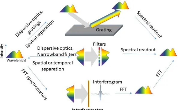
Figure 1.1 shows mechanism of three different spectrometers. Working principle of conventional spectrometer is shown in Figure 1.1 on top. In these types of spectrometers, gratings or prism are used to separate spectrum into colors before measuring their intensity. Second type of spectrometer is shown in Figure 1.1 in the middle path. In this spectrometer, tunable broad band filters are used instead of grating and intensity light passed through each filter is measured individually. Last type of spectrometer mechanism is shown in Figure 1.1 on the bottom. It has totally different working principle comparing to previous ones. In this type of spectrometers, no dispersive optical elements or filters are needed. Broad band light is sent directly to interferometer without being separated. The interferogram fringe patterns which contain information about spectrum are detected by moving the mirror. Taking Fast Fourier Transform of these fringe patterns, spectrum is reconstructed back. Further explanation will be discussed in chapter 6.1.
3
Figure 1. 1 Working principles of three different spectrometers are presented. On top grating based spectrometer is shown. Scheme in the middle presents narrowband filter spectrometer while figure at the bottom shows FFT spectrometers.
4
In this thesis, Fourier Transform Plasmon Resonance spectrometer is presented. We used a plasmonic interferometer to obtain spectroscopic information of light. Our spectrometer converts spatial interference pattern into spectroscopic information using Fast Fourier Transform Algorithm. We design a slit-grove or slit-ridge plasmon interferometer with varying optical path. Due to the varying optical path, the transmitted light yields a high contrast interference pattern which can be converted into spectroscopic information. In our design, there is no need for a bulky dispersive prism or dispersive optical elements. Our design is based on inherent coherence of the surface plasmons propagating through the subwavelength metal holes.
1.1 Organization of thesis
In this thesis, Fourier Transform Plasmon Resonance spectrometer is presented. The results of measurements are compared with the results of conventional spectrometer. Brief review of surface plasmon interferometers and physics lying behind the surface plasmons are also given in first chapters.
In Chapter 1, an introduction to surface plasmon resonance sensors and different types of spectrometer is made and motivation to Fourier Transform Plasmon Resonance is given.
In Chapter 2, optical properties of metal are theoretically explained. SPP excitation methods are also discussed.
Chapter 3 is a review of surface plasmon polaritons interferometer with experimental calculations
In Chapter 4, Focused ion beam (FIB), Electron induced deposition and application are briefly discussed.
In Chapter 5, we present subwavelength ridge-slit interferometer on gold made by FIB and electron induced deposition.
5
In Chapter 6, we present characterization of our Fourier Transform Plasmon Resonance spectrometer and compare them with the results of conventional spectrometer. Moreover, in this chapter both FTIR and static FTIR are discussed. In Chapter 7, we discuss the limitations FTPR spectrometer.
6
Chapter 2
2
Surface Plasmon Polaritons
Surface plasmon polaritons (SPP) are collective oscillation of electrons at the interface of dielectric and metal. The coupling of this oscillation with electromagnetic waves is called surface plasmon polaritons. Explaining the optical properties of metal will be a good step to understand SPP behavior.
2.1 Optical properties of noble metals
Optical properties of metals are dependent on frequency of incident light and can be described by complex dielectric function [6]. Electrons in conduction band generally considered as free electrons and they can move in bulk metal almost freely. Moreover, existence of electric field can oscillate these free electrons leading displacement of electron from their equilibrium point. Then individual electric dipoles are created. By adding all individual electric dipoles, polarization per unit volume is obtained. Polarization P is expressed by following equation.
𝑷(𝜔) = 𝜀0𝜒𝑒(𝜔)𝑬(𝜔) (1)
7
Due to the polarization, electric displacement takes place Electric displacement can be written as:
𝑫(𝜔) = 𝜀0𝜀(𝜔)𝑬(𝜔) = 𝜀0𝑬(𝜔) + 𝑷(𝜔) (2)
By substituting equation (1) to equation (2) we get following expression.
𝜀(𝜔) = 1 + 𝜒𝑒(𝜔) (3)
From equation (3), it is obvious that dielectric permittivity of metal is strongly dependent to the frequency of external electric field.
2.2 Drude-Sommerfeld theory
Considering only effects of free electron without including interband transition will be a good start to explain SPPs behavior. Drude-Sommerfeld model works well for free electrons in metal.
𝑚𝑒
𝜕2𝑟
𝜕𝑡2 + 𝑚𝑒Г
𝜕𝑟
𝜕𝑡 = 𝑒𝐸0𝑒−𝑖𝜔𝑡 (4)
me and e represents effective mass and charges of an electron respectively, frequency
and amplitude of applied electric field are noted by ω and E0. Г = vF/l where vF is
fermi velocity and l is the mean free path of electron between scattering events, and Г is proportional to damping term of the equation. Substituting r(t)=r0e-iωt to equation
(4) and using equation (3) we get:
𝜀𝐷𝑟𝑢𝑑𝑒(𝜔) = 1 − 𝜔𝑝2
𝜔2+ iГ𝜔 (5)
Where 𝜔𝑝 = √𝑛𝑒2/(𝑚
𝑒𝜀0) is plasma frequency. Equation (5) can be written in terms
8 𝜀𝐷𝑟𝑢𝑑𝑒(𝜔) = 1 − 𝜔𝑝 2 𝜔2 + Г2+ i Г𝜔𝑝2 𝜔(𝜔2+ Г2) (6)
By using the constant values of ωp and Г one can plot the imaginary and real part of
permittivity. Figure 2.1 shows experimentally obtained dielectric constants for silver which fits theoretical dielectric curves well. In this figure, we can see that real part of dielectric constant of silver is always negative, which makes refractive index strongly imaginary. Imaginary refractive index prevents light penetrating to large extend.
Figure 2.1 Graph of real and imaginary parts of dielectric constants of silver. Graph was calculated from experimental data of silver [7].
9
2.3 Interband transitions
Drude-Sommerfeld theory can explain the optical properties of metals infrared region. However, this theory is not enough to explain interband transition. Interband transition happens when the higher energy light is applied, typically around 2.5eV (500nm) for gold. Higher energy incident light can excite electrons from lower shells of the atom. These electrons are called bound electrons. Similar equation to Drude-Sommerfeld model with additional terms is used to explain optical behavior of metal including interband transition. Bound electrons excited from lower shells are not free, and they have restoring force.
𝑚𝜕2𝑟 𝜕𝑡2 + 𝑚𝛾
𝜕𝑟
𝜕𝑡+ 𝛼𝑟 = 𝑒𝐸0e−𝑖𝜔𝑡 (7)
Where m is effective mass of bound electron. Effective mass of bound electrons and effective mass of free electrons are generally different. γ represents damping constant of radiating bound electrons, while α is standing for spring constant of restoring force to keep electrons around the atom. Using same, r(t)=r0e-iωt substitution as we did in
previous chapter we get:
𝜀interband(𝜔) = 1 + ώ𝑝
2
(𝜔02+ 𝜔2) − 𝑖𝛾𝜔
(8)
Where ώ𝑝 = √𝑛̃𝑒2/𝑚𝜀
0. 𝑛̃ is bound electron density, ώp is plasma frequency and
𝜔0 = √𝛼/𝑚. As it is done above, equation is divided to real and imaginary parts as: 𝜀interband(𝜔) = 1 + ώ𝑝 2(𝜔 02− 𝜔2) (𝜔02 + 𝜔2)2− 𝛾2𝜔2 + 𝑖 𝛾ώ𝑝 2𝜔 (𝜔02+ 𝜔2)2− 𝛾2𝜔2 (9)
When interband transitions of bound electrons are also considered, experimental and theoretical data fit each other well. As mentioned early sections of this chapter,
10
interband transitions play significant role. Moreover, importance of this transition can be also seen from the equation (9)
2.4 Surface plasmon polaritons at plane interface
Collective oscillation of electrons at the surface or at the interface is called SPP. To understand SPPs we deal with the interface of two medium. One of the medium has complex, frequency dependent dielectric function while other medium has real dielectric function. To describe surface plasmon polaritons at plane interface, homogenous solution of Maxwell’s equation is used. Considering 𝑧 = 0 coincides with plane interface, solution for Maxwell’s equation will be:
∇×∇×𝐸(𝑟, 𝜔) −𝜔2
𝑐2 𝜀(𝑟, 𝜔)𝐸(𝑟, 𝜔) = 0 (10)
Where 𝜀(𝑟, 𝜔) = 𝜀1(𝜔) when 𝑧 < 0 and 𝜀(𝑟, 𝜔) = 𝜀2(𝜔) when 𝑧 > 0. Electromagnetic field exponentially decreases on both sides of the interface with the increasing distance from interface. In this point, just p-polarization is examined, since s-polarized electromagnetic wave do not excite SPP. P-polarized plane waves are on both upper and lower parts of the interface. In another word, it is on both half spaces. For half spaces j can be taken as 𝑗 = 1 and 𝑗 = 2 and equation can be written as:
𝐸𝑖 = ( 𝐸𝑗,𝑥
0 𝐸𝑗,𝑧
) 𝑒𝑖𝑘𝑥𝑥−𝑖𝜔𝑡𝑒𝑖𝑘𝑗,𝑧𝑧, 𝑗 = 1, 2. (11)
Wavevector component will be held by following relation
𝑘𝑥2+ 𝑘𝑗,𝑧2 = 𝜀𝑗𝑘2, 𝑗 = 1, 2. (12)
Here 𝑘 = 2𝜋/𝜆, λ is wavelength in vacuum. Displacement field is not affected by source ∇ ∙ 𝐷 = 0. This condition is given as:
11
𝑘𝑥𝐸𝑗,𝑥+ 𝑘𝑗,𝑧𝐸𝑗,𝑧 = 0, 𝑗 = 1, 2. (13) This helps to write equation (11) as:
𝐸𝑗 = ( 1 0 −𝑘𝑥 𝑘𝑗,𝑧 ⁄ ) 𝑒 𝑖𝑘𝑗,𝑧𝑧, 𝑗 = 1, 2 (14)
To simplify, the notation 𝑒𝑖𝑘𝑥𝑥−𝑖𝜔𝑡is omitted. Boundary conditions should match and function should be continuous at the boundaries to solve the equation. So, component of electric field which is parallel to the interface and component electric displacement which is perpendicular to the interface should be continuous. Then the next equation can be written as:
𝐸1,𝑥− 𝐸2,𝑥= 0
𝜀1𝐸1,𝑥− 𝜀2𝐸2,𝑧 = 0 (15)
Equations (13) and (15) will form four homogenous equations to calculate four unknown components. Possible solutions are obtained when determinant is zero. First solution of equations is when 𝑘𝑥= 0 and this does not explain excitation on the
interface. Second solution is held when:
𝜀1𝑘2,𝑧− 𝜀2𝑘1,𝑧 = 0 (16)
From the combination of equation (12) and equation (16) and substituting 𝑘 = 𝜔 𝑐⁄ we get: 𝑘𝑥2 = 𝜀1𝜀2 𝜀1+ 𝜀2𝑘2 = 𝜀1𝜀2 𝜀1+ 𝜀2 𝜔2 𝑐2 (17)
12 𝑘𝑗,𝑧2 = 𝜀𝑗
2
𝜀1+ 𝜀2𝑘2 𝑗 = 1,2 (18) From equations (17) and (18) conditions for the existence of interface mode are derived. Imaginary part of dielectric function is taken as small to neglect them so solution for the equation will be easy. Since we are looking propagating wave at the interface, 𝑘𝑥2 in equation (17) should not be imaginary. To fulfill this condition both
product and sum of the dielectric functions should be both negative or positive. Moreover, to obtain solutions at the boundary of the interface, wavevector should be imaginary because of anticipated exponential decay. Wavevector will be imaginary when denominator of equation (18) is negative. Then the final conditions to get wave mode at the interface are:
𝜀1(𝜔) ∙ 𝜀2(𝜔) < 0 (19)
𝜀1(𝜔) + 𝜀2(𝜔) < 0 (20)
Here one of the dielectric functions must be negative and greater in magnitude than other. This condition will be held at the interface of noble metals such as gold and silver and some dielectric materials such as glass and air.
2.5 Properties of surface plasmon polaritons
In this part of the chapter properties of surface plasmon polaritons is discussed. Same equations from the previous chapters will be used to explain surface plasmon polaritons. We will consider the imaginary part of dielectric constant of metal due to scatterings and other types of loses. Let’s take dielectric constant of metal as:
13 Here both 𝜀′
1 and 𝜀˝1are real. SPPs propagation happens at metal dielectric interface.
We assume that our dielectric material has real dielectric constant, 𝜀2, to avoid energy losses.
Because of the close relation between dielectric constant and wavenumber, complex wavenumber can be written as 𝑘𝑥= 𝑘′
𝑥+ 𝑖𝑘˝1. SPP wavenumber is determined by
the real part of wavenumber whereas imaginary part of wavenumber stands for the damping of SPP propagation at the interface. Using equation (17) and assuming 𝜀̀1 ≫
𝜀˝1 real and imaginary parts of 𝑘𝑥 are calculated as:
𝑘′ 𝑥≈ √ 𝜀′ 1𝜀2 𝜀′ 1+ 𝜀2 𝜔 𝑐 (22) 𝑘˝𝑥 ≈ √ 𝜀′ 1𝜀2 𝜀′ 1+ 𝜀2 𝜀˝1𝜀2 2𝜀′ 1(𝜀′1+ 𝜀2) 𝜔 𝑐 (23)
From equation (17) wavelength of SPP is written as:
𝜆𝑆𝑃𝑃= 2𝜋 𝑘′ 𝑥≈ √ 𝜀′ 1 + 𝜀2 𝜀′ 1𝜀2 𝜆 (24)
Here λ is the wavelength of light in vacuum.
𝑘˝𝑥 defines propagation length of SPP along the interface and at the same time it is responsible for exponential decay of the electric field amplitude. This decay is main source of heat generated in metal. The equation for decay length from the interface is calculated by using equation (18) as:
𝑘1,𝑥 =𝜔 𝑐 √ 𝜀′ 12 𝜀′ 1+ 𝜀2[1 + 𝑖 𝜀˝1 2𝜀′ 1] (25)
14 𝑘1,𝑥 =𝜔 𝑐 √ 𝜀22 𝜀′ 1+ 𝜀2[1 − 𝑖 𝜀˝1 2(𝜀′ 1+ 𝜀2)] (26)
2.6 Excitation of surface plasmon polaritons
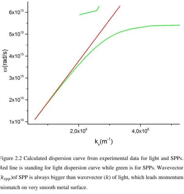
Surface plasmon polaritons are propagating surface plasmons excited by external applied electric field. However, to excite SPPs, energy and momentum conservation should be fulfilled. Just illuminating light on material which has very smooth surface will not excite any plasmon polaritons, because of momentum mismatch. Figure 2.2 shows dispersion curves of light and SPPs. Dispersion curve light is shown in red while dispersion curve of SPPs is in green. From the graph in Figure 2.2 it is obvious that these two curves never meet with each other and SPPs wavevector (𝑘𝑠𝑝𝑝) is
always bigger than wavevector of light(𝑘). This is the explanation where momentum mismatch comes from. In order to excite SPPs one should overcome momentum mismatch first. There are two ways such as prism coupling and grating coupling to overcome this issue.
15
Figure 2.2 Calculated dispersion curve from experimental data for light and SPPs. Red line is standing for light dispersion curve while green is for SPPs. Wavevector (𝑘𝑠𝑝𝑝)of SPP is always bigger than wavevector (𝑘) of light, which leads momentum mismatch on very smooth metal surface.
16
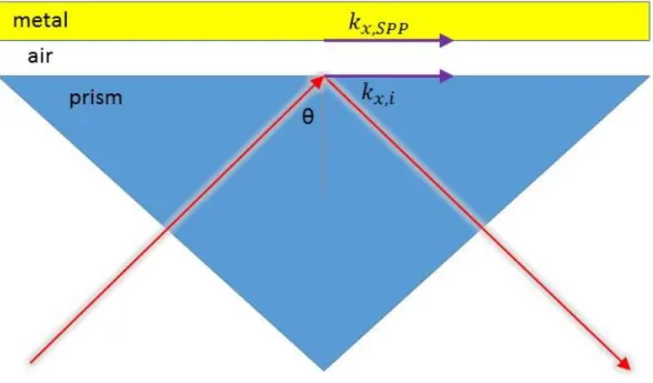
Prism coupling is extensively used method to excite SPP. Although there are two types of prism coupling, their working principles are almost same. First type is Otto configuration[8]. In Otto configuration, there is a gap between metal and prism. See Figure 2.3. Incident light is shown in red. At a critical angle, evanescent wave will be observed on the surface of prism and the tail of evanescent wave will excite the SPP. In figure 2.3 excited SPP is shown in violet. However, the gap between metal and glass should be arranged precisely to excite SPPs.
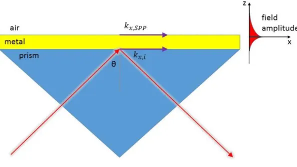
Kretschmann configuration is an alternative method to Otto configuration[9]. In Kretschmann configuration metal is directly evaporated on prism instead of having a gap between metal and prism as shown in Figure 2.4 [10]. This method solved the gap controlling problem. In this configuration thickness of metal should be controlled precisely, which is easy comparing to gap controlling in Otto configuration. Thickness of metal is important, since when it is too thin SPP will be damped very fast and when metal is to thick SPP cannot be excited due to the absorption.
In both Kretschmann and Otto configurations reflection of light detected to understand weather SPP is excited or not. When SPPs are excited, intensity of reflected light will be minimum. Minimum intensity is due to the destructive interference of surface plasmon and the reflected light. Moreover, when broad band wavelength is used, wavelength which is not reflected, considered to be converted to surface plasmon polaritons [6]. Both of these ways are widely used to observe biomolecular sensing and chemical interactions of specimen between metal.
17
Figure 2.3 Otto configuration. Blue triangle stands for prism while yellow rectangle stands for thin gold metal film. Red line is incident light and violet lines show excited SPP. In Otto configuration, there is a gap between thin metal film and prism
18
Figure 2.4 Kretschmann configuration. Blue triangle stands for prism while yellow rectangle stands for deposited thin gold metal film. Red line is incident light and violet lines stand for excited SPP.
19
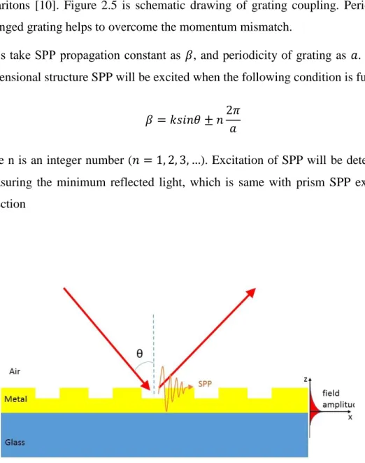
Patterning the surface of the material is another way to excite the surface plasmons polaritons [10]. Figure 2.5 is schematic drawing of grating coupling. Periodically arranged grating helps to overcome the momentum mismatch.
Let’s take SPP propagation constant as 𝛽, and periodicity of grating as 𝑎. For one dimensional structure SPP will be excited when the following condition is fulfilled:
𝛽 = 𝑘𝑠𝑖𝑛𝜃 ± 𝑛2𝜋
𝑎 (27)
Here n is an integer number (𝑛 = 1, 2, 3, …). Excitation of SPP will be detected by measuring the minimum reflected light, which is same with prism SPP excitation detection
Figure 2.5 Schematic of grating coupling. To overcome momentum mismatch, periodical grooves are etched on the surface of metals. Impinging photons can excite SPP as shown in the figure.
20
Surface roughness and small defects are another way to excite SPP [11]. There is no need for grating which is an array of grooves or ridges on metal. SPP can be also excited using just ridge or groove instead of arrays, when phase matching condition is fulfilled:
𝛽 = 𝑘𝑠𝑖𝑛𝜃 ± ∆𝑘𝑥
(28)
Effects of groove and ridge on SPP are theoretically studied by G. Brucoli et. al. [11]. According to their study the depth of groove and height of the ridge are very important for the excitation of SPP.
2.7 Application of surface plasmon resonance
During the last four decades, we have seen development of optical sensors in research on biological interactions and chemical reactions. Some of the common sensors are ellipsometry, spectroscopy, interferometry and SPR sensors. Principle of all these sensors to measure absorbance, fluorescence properties of molecules and refractive index of medium. The main idea of this thesis is based on SPR sensors and following paragraphs mainly focus on applications of SPR sensors.
Potential of SPR sensors was recognized by I. Pockrand et. al in 1978 [12]. In addition, Gordon et. al. also observed process at the interface of the metal by looking attenuated total reflection (ATR) of impinging light [13]. In one of the studies in 1982 gas detection was also achieved using SPR sensors [14]. Since then scientists continuously doing researches on SPR sensors, they come up with different types of SPR sensors. Moreover, some of them even commercialized by several companies [15].
First type of SPR sensor is based on ATR method. In this method Kretschmann configuration is used and incident monochromatic light reflected at the interface of prism and thin metal layer. At critical angle this light evanescently tunnels the thin metal and excited SPR on the outer boundary of the metal[15]. Excitation of SPR will
21
happen at a critical angle and intensity of reflected light will be minimum at this angle. Since SPR is very sensitive to the medium, changes in the medium will change the angle of minimum intensity reflection.
Using SPR sensors concentration of chemical species can be found in liquid and gas without help of any reagent. Concentration of ethanol in water was calculated by this method[16]. Moreover, ATR based sensors also used to monitor biomolecular interaction on the surface of the metal. This study shows that SPR sensors can detect not only the concentration but also binding specificity and kinetic constants [17]. Kretschmann prism coupling was used and with broad band light for biosensing. Refractive index is determined from the changing resonance wavelength [18]. Although grating coupling sensors are not used as widely as prism coupling sensors, they have some advantages on prism coupling. Grating coupling sensors are easy to produce and low cost fabrication comparing to prism coupling sensors [19, 20]. In 2001 SPR based grating coupling device was presented by Brockman and Fernandez [20] . In their study, they used four hundred array sensing gold channels coated on plastic chip. Reflected light detected by CCD camera. This system further improved by other groups to detect antibody [21].
22
Chapter 3
3
Plasmonic Interferometers
In this chapter of thesis plasmon interferometers are presented. There are many studies and applications of surface plasmon interferometers [22-24]. SPPs are electromagnetic waves propagating on the surface of a metal and thus they can interfere constructively and destructively. As in the case of electromagnetic interferometry, high contrast constructive and destructive interferences strongly dependent on relative phase. In plasmonic interferometers, high contrast interference patterns are obtained due to the extraordinary transmission though the subwavelength aperture or slit. This extraordinary phenomenon is first observed by Ebbesen et. al. In their work, they have shown that SPP plays a very important role in transmission through subwavelength holes.
To understand how SPP interferometer works, extraordinary transmission through a subwavelength aperture should be understood first. In the following section, we will explain extraordinary transmission phenomenon.
3.1 Extraordinary transmission through subwavelength apertures
The extraordinary transmission firstly observed by Ebbesen et. al. They used subwavelength aperture arrays to observe extraordinary transmission phenomenon
23
[3]. This phenomenon has attracted attention of many researchers and they come up with many other geometrical corrugations such as hole arrays [25, 26] and holes surrounded by circular surface corrugations [27]. Moreover, light transmission through subwavelength apertures has been theoretically investigated [28].
Light can be described by a wave and a particle and thus diffraction theory can be used to explain light. However, diffraction of light is really complex even for very simple geometrical shapes of apertures, although transmission through aperture on opaque material is studied more than hundred years. Diffraction theory is explained in many books with different aspects [29]. We will discuss transmission through aperture for two cases. The first case is when the radius of aperture is larger than wavelength (𝑟 ≫ 𝜆). This phenomenon can be explained by classical diffraction theory [10]. Huygens-Fresnel principle can be used to study the nature of transition when radius of aperture is larger than the wavelength of light. When the radius of aperture much bigger than wavelength of impinging photons, transmission trough aperture will be 𝑇 ≈ 1. We are not interested with this case. Extraordinary transmission occurs when 𝑟 ≪ 𝜆.
There is analytical solution of transmission through subwavelength aperture suggested by Bethe and Bouwkamp for infinitely thin opaque metal [30, 31]. To have infinitely thin and opaque metal, conductivity of metal should be also infinite. However, this transmission is not allowed because real metal has finite thickness and conductivity. Moreover, opaque metal has thickness on the order of several skin depths and when material is thick enough, tunneling of the radiation is not allowed. Therefore, localized surface plasmons significantly influence the transmission phenomenon.
The light transmitted through the subwavelength circular holes was at least 2-3 times larger than classically expected transmission of light. This cannot be explained by just considering diffraction theory. The fact that transmitted light was higher than classically expected transmission suggests that transmission phenomenon is mediated
24
by SPP through the aperture [3, 32]. Moreover, extraordinary transmission is strongly dependent on shape of aperture, depth of groove and height of ridge [11, 32].
This phenomenon can be also observed using single aperture surrounded by ridges, grooves or any other corrugations with different geometrical shapes. One of the interesting surface corrugation is bull’s eye, centric hole surrounded with circular grooves [33]. Grooves excite SPPs and it travels towards the hole and tunnels through the hole exciting far field electromagnetic wave.
In one of the previous studies, instead of holes, arrays of gratings were used to fulfill the phase matching of the SPPs with the incident beam light. In this experiment, they played with groove height in order to tune efficiency of coupling
To increase the transmission, geometrical dimensions of apertures can be optimized. By playing with geometry of nanoaperture, it is possible to determine the spectral position of localized surface plasmon (LSP). Due to the field enhancement at the edge of the aperture, transmission is increased. Moreover, using high index dielectric material and multilayer structures it is also possible to improve transmission through subwavelength aperture.
3.2 Plasmon interferometer
When light illuminated on a slit-groove interferometer, wavefront component on the groove, 𝐸𝐺, partially scatters SPP, which propagates towards the slit. Initial amplitude
of scattered SPP is given by groove scattering coefficient, 𝛽𝐺. Reaching the slit after propagating distance d, SPP gains an additional phase [34]
𝜓(𝑑, 𝜃) = 𝑘𝑆𝑃𝑃𝑑 − 𝑘0sin(𝜃) 𝑑 + 𝜙1 (29) Where 𝑘0 and 𝑘𝑆𝑃𝑃 are complex wavenumbers for free space and for SPP, respectively. θ represents an angle of incidence, while 𝜙1 is total phase gained during the scattering. SPP interferes with 𝐸𝑆, which is component of wavefront on the slit. Total intensity 𝐼𝑆𝐺 transmitted through the slit groove interferometer is given by:
25
𝐼𝑆𝐺(𝑑, 𝜔) = 〈|𝐸𝑆(𝜔) + 𝛽𝐺𝐸𝐺(𝜔)𝑒𝑖𝜓(𝑑,𝜃)| 2
〉 (30)
𝐼𝑆𝐺(𝑑, 𝜔) = 𝐼𝑆(𝜔) + 𝛽𝐺2𝐼𝐺(𝜔)𝑒−𝛼𝑑+ 2𝛽𝐺𝑒−𝛼𝑑/2|𝑊𝑆𝐺(𝜔)|𝑐𝑜𝑠{𝑅𝑒𝜓(𝑑, 𝜃)} (31) Where 𝜔 = 𝑐𝑘0, c is speed of light in vacuum, 𝛼 is absorption coefficient of SPP,
𝐼𝑆(𝜔) = 〈𝐸𝑆∗(𝜔)𝐸𝑆(𝜔)〉 and 𝐼𝐺(𝜔) = 𝐸𝐺∗(𝜔)𝐸𝐺(𝜔) are spectral densities of incident
wavefront on slit and groove, |𝑊𝑆𝐺(𝜔)| = 〈𝐸𝑆∗(𝜔)𝐸𝐺(𝜔)〉, is cross spectral density relating the two field with angle brackets indicating averaging. In their study, Drew Morrill et. al. [34] measured quantity of 𝐼𝑆(𝜔) using an isolated slit. Assuming
𝐼𝑆(𝜔) = 𝐼𝐺(𝜔), and normalizing equation 31 to 𝐼𝑆(𝜔), normalized transmitted
intensity, 𝐼𝑛(𝑑, 𝜔), is generated:
𝐼𝑛(𝑑, 𝜔) = 1 + 𝛽𝐺2𝑒−𝛼𝑑+ 2𝛽𝐺𝑒−𝛼𝑑/2|µ(𝑑, 𝜔)|𝑐𝑜𝑠{𝑅𝑒𝜓(𝑑, 𝜃)} (32) Here µ(𝑑, 𝜔) is spatial degree of coherence. The magnitude of µ(𝑑, 𝜔) is obtained from experimental data, determining visibility of the interference fringes:
µ(𝑑, 𝜔) = 𝑣(𝑑, 𝜔) =|𝐼𝑚𝑎𝑥− 𝐼𝑚𝑖𝑛|
4𝛽𝐺𝑒−𝛼𝑑/2 (33)
𝐼𝑚𝑎𝑥 and 𝐼𝑚𝑖𝑛 are the maximum and minimum intensities after normalization,
26
Figure 3.1 Incident beam is shown by red arrows while excited SPP is shown by a violet arrow. Polarization of the incident beam is polarized perpendicular to the groove line.
27
3.3 Application of extraordinary transmission
In the last part of plasmonic interferometer we will discuss extraordinary transmission and their applications as sensors. Extraordinary transmission is explained in our previous chapter. Many scientist come up with different methods based on nanohole arrays [35-37] and different applications of this transmission phenomenon.
In addition to nanohole arrays, slit-groove pairs also play a very important role in transmission and hence high contrast interferometry can be achieved. This slit-groove interferometers have also many applications [38, 39]. Surface plasmon interferometry, where slit groove pairs etched by focused ion beam, is also used to measure the group velocity of surface plasmon [39].
Plasmon interferometer is one of the very sensitive methods used to understand binding of molecules on surface. In one of the recent works sensing using refractive index has become very popular [40]. By observing the shift of the valleys of the interference high sensitivity is reported.
Feng et al used parallel groove slit groove configuration [5]. Multi-wavelength light is illuminated on the surface of GSG configuration and transmitted light directly observed through the slit. Transmitted light depends on the slit groove distance and wavelength of light. This sensor has very small sensing volume in several tens of femto liters.
One of the interferometry application is to measure the refractive index [1, 41]. Refractive index of ionic liquid is calculated by Yavas and Kocabas [1]. They have used slit-groove pairs on gold with small angle between them. SPPs excited from the groove interfere with SPP on slit and give high contrast interference fringes. From the period of this fringes refractive index of liquid can be calculated.
28
Chapter 4
4
Focused Ion Beam (FIB) and
Electron Beam Induced Deposition
(EBID)
4.1 Focused Ion Beam (FIB)
Focused Ion Beam (FIB) is technique used for ablation and deposition. By using FIB nano 3D shapes can be created. In principle, FIB is very similar to Scanning Electron Microscope (SEM), the only difference between them is the ion source, which is used in FIB, instead of electron source in SEM [42]. FIB instrument contains ion column, detectors, gas inlets, computer, ion sources and vacuum system. It contains three vacuum chamber. One pumping region is for ion source and ion column. Pressure inside the ion column is 10-8 torr. High vacuum is required to prevent the ion source
from contamination. Second pumping region is for the detector. Last vacuum region is sample chamber where sample is held. To increase the mean free path of ion, high vacuum system is required. Otherwise, ions in the chamber will interact with junk
29
molecules inside the chamber and thus meaning of free path of the ions will be diminished.
Liquid ion sources are used in FIB. Ga is a very common ion source because of its low melting point. First ion source is melted and very high electric field is applied to ionize the liquid Ga. To accelerate ions, potential difference is applied and energetic ions transferred to the chamber through tungsten needle. Typical applied voltage to accelerate the Ga+ range from 1keV to 50keV and current can vary from 1pA up to 10-20nA. To control the direction of ions, electromagnetic coils are used. Moreover, FIB has movable stage similar to SEM. Stage can move in x, y, z directions and can also rotate 3600.
Two types of detectors are commonly employed in FIB instrument. One detector is used to detect secondary electrons while other is used to detect secondary ions to image. In either case, applying large current is risky since ions are very massive comparing to the electron and they are destructive. Ion milling and etching starts even in very small applied current.
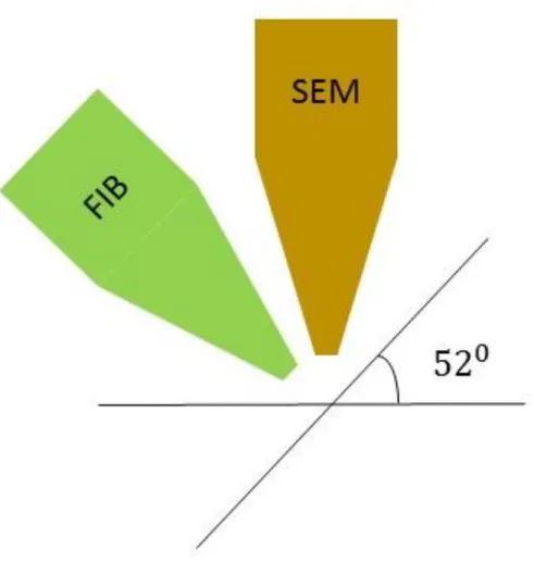
FIB instruments have dual platform column, where both electron and ion columns are located inside the chamber as shown in Figure 4.1. Electron column is needed to use the equipment as SEM to prevent the sample from being etched while imaging and FIB column is used for milling and etching. Angle between electron and ion column is 520. Sample can be tilted 520 to make ion gun perpendicular to sample.
30
Figure 4.1 Schematic illustration of dual platform FIB. The angle between FIB and SEM is 520. Sample is tilted 520 to make FIB column perpendicular to the sample
31
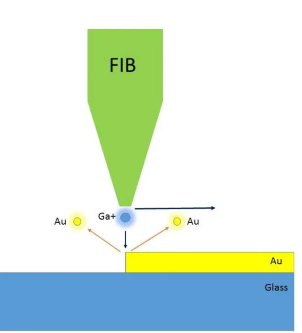
When accelerated ion particles interact with solid sample several processes takes place. Some of the ions will enter the solid and slow down while other ions are backscattered. Moreover, collision of ions may lead to defect formation, electron or photon excitation [43]. In addition, ion collusion leads amorphization, crystallization, phase transformation and sputtering.
Energetic incident ion on solid surface transfers its kinetic energy to the atom of the solid. During this process, some of the atoms will be ejected from the surface of the solid. Many of these ejected atoms are generally neutral atoms and some of them are positively and negatively charged ions [43]. Figure 4.2 shows schematic representation of etching process in FIB. Incident accelerated ions are Ga+ ions shown with blue and ejected gold atoms are shown in yellow. FIB is scanning from left to right.
32
Figure 4.2 Schematic representation of the working principle of a focused ion beam. Highly energetic Ga+ ions are focused on a gold thin film on a glass surface to generate localized gold etching.
33
4.2 Electron induced beam deposition
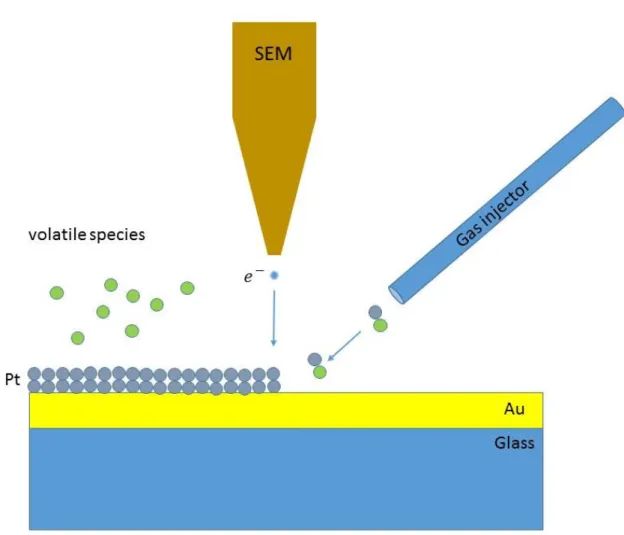
While using SEM for imaging, it is possible to see that the surface of the sample is contaminated. This is because of the deposition of junk atoms inside the chamber. This is unintentional deposition. However, carefully arranging gas injection controlled deposition is possible and it has very useful applications. Decomposition of gaseous molecules by electron beam and deposition of non-volatile fragment is called electron beam induced deposition (EBID). SEM and STEM are both used as accelerated electron provider. SEM has high accuracy and thus very smooth structures can be achieved. Precise nano 3D and complex structures [44] also created using EBID.
As gas injection precursor, liquid, solid and gasified materials are used. These materials are evaporated before they are introduced to the high vacuum chamber. Electron energy can decompose the molecules and deposit, generally secondary electrons are used to decompose. Figure 4.3 shows deposition mechanism of EBID. Gas precursor injects gaseous molecules and hence accelerated electrons decompose molecules. Non-volatile species are deposited on the surface while volatile species are pumped out.
There are wide variety of precursor materials used for FIB induced deposition but in this thesis, we only used Pt source. Although dual platform FIB is very precise and easy to control, a fabrication with FIB is a sequential process and thus large are fabrication is impossible and it is time consuming.
34
Figure 4.3 Schematic illustration of electron induced deposition of Pt on Au. Electrons decompose gas molecules coming from gas injector and therefore non-volatile species will be deposited while non-volatile species will be pumped out.
35
4.3 Focused Ion Beam applications
Nowadays, nanostructure fabrication becomes one of the essential part of nanotechnology and nanoscience since photolithography has limits around its wavelength of exposing beam. Moreover, photolithography needs a mask while FIB does not need any mask [45] to make nanofabrication on solid. FIB can etch sub 5nm structure which makes it very useful in fabricating nanostructures [46].
A. Hemamouche et. al. presented nanoholes and nanomasks on the surface of freestanding Si, SiN and SiO2 which have few tens of nanometers thickness. They
also make nanopores on atomically thin graphene and hexagonal boron nitride. It is claimed that FIB can reproducibly fabricate sub 10nm holes on these materials and this is reproducible.
Creating nanoholes on freestanding graphene can be used for gas permeation [47]. Celebi et. al. presented nanopores on the surface of freestanding graphene and they used for gas sieving.
Nanostructures fabricated by FIB are used to develop nanoimprint masks [48]. By etching Si with FIB and taking the replica of the surface of Si using PDMS they calculated the depth of nanochannels and nanoholes. The fabricated nanostructures on Si can be used many times.
36
Chapter 5
5
Fabrication
of
Plasmon
Interferometer using Focused Ion
Beam (FIB)
There are many sensor applications of surface plasmon polaritons. One of these sensor applications is plasmonic interferometer. Generally, plasmonic interferometers have slit-groove pairs created on a thin metal surface using FIB [49]. Groove is the main source to excite SPPs while the transmission of light is observed through the slit.
In this part of thesis slit-ridge interferometer on thin gold metal is presented. A slit on a gold thin metal surface is written by using FIB and Pt ridge is deposited by using EBID. Almost all of the plasmonic interferometers have slit-groove pairs, but we replaced groove with platinum ridge. Pt ridge efficiently excites SPPs and high contrast interference patterns are observed.
We used thermal evaporator to evaporate gold on glass and got very smooth 160nm thick gold film on the surface of glass. After thermal evaporation, gold film is etched
37
with FIB and Pt ridge is deposited using EBID. Figure 4.1 is a schematic representation of slit-ridge interferometer. Yellow thin film is gold on glass, and gap between films shows the etched slit. Blue rectangular line stands for deposited Pt ridge.
Figure 5.1 Schematic representation of ridge-groove interferometer. Yellow color represents Au on glass and gap between gold films is a slit etched by FIB. Blue long cuboid is deposited ridge and angle between ridge and slit is 50.
38
5.1 Fabrication
Many experimental studies showed that the thickness of metal is very important and in order to have high contrast fringes, generally the thickness of metal thin film is around 200nm [38, 50]. In our interferometer device, thickness of gold film was 180 nm which is enough. We used FIB with Ga+ source to etch slit. We do not apply high current to Ga+ ions in order to avoid destructive etching. To etch efficiently we always keep voltage (30kV) and current (28pA) fixed. We only controlled the dimensions of slit with dwell time without changing the voltage and current. It should be noted here that dwell time is the time spend by incoming beam in the same position point.
We used dual platform FIB instrument in UNAM to deposit platinum ridge. As discussed in the 4th chapter, dual platform FIB instrument has both electron and ion columns. In this FIB instrument, both electron beam induced deposition and ion beam induced deposition can be done. Without taking out the sample from the chamber after the etching process we can immediately deposit Pt on the gold surface. We used electron induced deposition. Applied voltage and current of SEM were 5kV and 1.6nA, respectively. In deposition process, we have controlled the height of Pt ridge is controlled by dwell time as in the etching process.
Another good thing with this machine is that high quality SEM images can be simultaneously obtained. Figure 4.2 is a SEM image of a slit and the Pt ridge. The lengths of both ridge and slit are 150µm and scale bar is 20 µm.
39
Figure 5.2 A SEM image of a ridge-slit. Lengths of both Pt ridge and slit are 150µm and scale bare is 20 µm. Left solid line is platinum ridge and groove line is slit etched by FIB.
40
5.2 Experimental setup
In our experiment, we used laser with a wavelength 635nm and the visible part of the electromagnetic spectrum. Figure 4.1 shows the schematic illustration of our experimental setup. Light is monochromatic and polarized. It is important to notify that the incoming light should be perpendicularly polarized to our ridge to support SPPs. The Pt ridge on gold interferometer, is the main source to excite SPPs and to overcome momentum mismatch. SPPs are excited on Pt ridge and travel towards the subwavelength slit aperture. When SPPs reach to the slit, they tunnel through the subwavelength aperture. Since SPPs can scatter into the far field, they can be observed in the commercial optical microscope. We have collected the light using 20X objective of optical microscope. Before light reaches to CCD camera we have magnified the image 1.5 times.
41
Figure 5.3 Schematic illustration of the experimental setup used to image SPPs on the gold surface. Laser (635nm) is used as a monochromatic light source. Polarizer is used to polarize the light coming from the laser. Light scattered from the interference fringes is collected by an objective and sent to a CCD camera. CCD camera captures the optical image of the interference pattern.
42
5.3 Results
In this chapter of Thesis, we demonstrate an interferometer with a subwavelength ridge and groove. There are many examples in the literature about the slit-groove pairs but there is not any study about the slit-ridge interferometers [23]. We show fabrication advantages of slit-ridge interferometers. Controlling the height of deposited ridge is easier than controlling the depth of groove. Moreover, we observed very high contrast interference fringes using slit-ridge pairs.
Basically, we have used the experimental setup discussed above. The length of both slit and ridge is 100µm and angle between them is 50. Monochromatic laser is used to excite SPPs. Excited SPPs on the ridge travel towards the slit and we see constructive and destructive interference patterns. When SPPs reach the slit they tunnel through the slit and excite far field electromagnetic wave which can be observed by an optical microscope. The image is taken by using a CCD camera. Due to the constructive and destructive interferences of SPPs, we observed high contrast interference fringes. Interference fringe patterns are shown in Figure 4.4 a). We have taken a line profile of the fringe patterns and get an interferogram of image. The interferogram is shown in Figure 4.4 b). By looking at Figure 4.4 a and b, it is easy to conclude that we have very high contrast interference fringes.
43
Figure 5.4 a) An image of interference fringes on the interferometry taken by CCD camera. b) The interferogram of the optical image.
44
5.4 Optimum thickness of platinum ridge for high contrast interference fringes
To find out the optimum height for high contrast fringes, we write array of slit-ridge pairs. We keep the dimensions of slit fixed and change the thickness of ridge. We create six slit-ridge arrays with lengths 100µm and thicknesses t=20nm, 35nm, 80nm, 100nm, 135nm and 200nm. Figure 5.5 a) shows the interferogram of six interferometers on the same sample. From left to right, the thickness of the ridge increases. It is obvious that central interferometers have very high contrast interference patterns. As we have done before we took images of interferogram. In order to calculate the contrast of fringes we used Michelson contrast formula [51]:
𝐶𝑜𝑛𝑡𝑟𝑎𝑠𝑡 =𝐼𝑚𝑎𝑥 − 𝐼𝑚𝑖𝑛
𝐼𝑚𝑎𝑥 + 𝐼𝑚𝑖𝑛 (34)
We took average of maximum and minimum point on the interferogram and by using the formula above we calculate the contrast for each interferometer. Contrast versus height graph is shown in Figure 5.5 b). In the graph, it is clear that the highest contrast is achieved at the ridge thickness of 80-100nm. We keep the width of the Pt ridge same and it was around 130nm. Theoretically expected height to efficiently excite SPPs was 100nm [11]. We have compared our result with the result of our previous work [1]. We showed contrast of slit-ridge interferometer with dashed orange line in Figure 5.5 b), and it is showing that ridge-slit interferometer contrast is very high comparing to slit-groove interferometer. Moreover, after we found optimum height, we used it in all of our following experiments.
45
Figure 5.5 a) Optical images of interference patterns on the ridge-slit pairs. Six slit ridge pairs are presented with varying height (t=20nm, 35nm, 80nm, 100nm, 135nm and 200nm). b) Contrast thickness graph, maximum contrast achieved at thickness t=80-100nm and orange dashed line shows contrast achieved from slit-groove pairs from our previous work.
46
5.5 Plasmonic decay
It is well known that SPPs decay exponentially into the dielectric and metal media. To observe decay of SPP, we fabricate slit and ridge of interferometer 200µm long, which is two times longer than the length of our previous interferometers. The lengths of both slit and ridge have been increased up to 200µm. Some part of SPPs is converted to heat during the travel at the metal dielectric interface. Increasing the length of the interferometer will be good solution to observe the decay of SPPs, since SPPs decay with increasing distance.
To analyze interferometer, we used the same setup. Optical images of interferometer are shown in Figure 4.6 a. By following the same process, we took a line profile to get an interferogram of the images. In Figure 4.6 b, it is noticeable that intensity of SPPs decreases with the increase in distance. We have observed collective oscillation of SPPs which is due to the oscillation come from diffraction of laser.
In addition, we calculated variation of contrast with the distance between the ridge and slit. As the distance increases, a decrease in the contrast of the image is expected. Length of the interferogram does not give the real distance travelled by SPPs, since SPPs excited on ridge and travel towards the slit. In order to find real distance travelled by SPPs, we multiplied the length of interferogram with a sinus of 5º, which is an angle between the slit and the ridge. After this multiplication, we calculated the contrast using the same Michelson contrast formula and plotted the contrast distance graph in Figure 4.6 c). In this graph, distinct decay in intensity is clearly observed.
47
Figure 5.6 a) 200µm long slit-ridge optical interference image. b) A line profile of the image. c) These is a decrease in the contrast with the increasing distance between the ridge and the slit.
48
Chapter 6
6
Fourier
Transform
Plasmon
Resonance (FTPR) spectrometer
6.1 Fourier Transform Infrared spectrometer
The history of Fourier Transform Infrared Spectroscopy goes back to 1880s. In 1880s, Michelson invented an interferometer, which is known as Michelson interferometer. Using his interferometer, he accurately measured wavelengths of light, and he was awarded Noble Prize in physics in 1907. In fact, the discovered interferometer is designed to examine the existence of aether (medium where light waves propagate), and as a result Michelson showed that aether does not exist [52]. Michelson knew the potential of interferometer to obtain the spectrum, but time consuming calculations are needed to convert interferogram to spectrum. The invention of computers made Fourier transform calculations faster. J. W. Cooley J. W. Tukey invented the Fast Fourier Transform algorithm which is a mathematical algorithm. Joining of microcomputers and FFT algorithm leads to the development of FTIR that we know today.
49
An interferometer measures the interference of light. Incident light is first split by a beam splitter. Reflected lights from the movable and fixed mirrors recombine back. Half of the incident beam travels towards the detector. Beam interference is detected by a detector because of the path difference between the reflected lights from two mirrors.
The most famous interferometer design is Michelson interferometer. Michelson interferometer generally consists of one light source, one fixed and one movable mirror. Right arm of interferometer also includes detector as shown in Figure 6.1. Beam splitter is located at the center of the interferometer[52]. It partially transmits and reflects the beam. Beams reflected from both movable and fixed mirror recombine at the beam splitter and travel together towards the detector. Recombination of beams is a simple process, and it is just interference of light. When amplitudes of light interfere constructively, overall amplitude will become larger and when they interfere destructively, overall amplitude becomes smaller.
To theoretically calculate the optical path difference and interference, we assume that our source sends monochromatic light beam. We will get constructive interference when the optical path difference is 𝛿 = 𝑛𝜆. At the same time, we will get destructive interference when optical path difference is 𝛿 = (12+ 𝑛)𝜆. Here n is an integer number and λ is wavelength of beam light. To achieve constructive path difference, mirror should move with distance 𝛿 = 𝑛𝜆 and to achieve destructive interference mirror should be moved to distance 𝛿 = (12+ 𝑛)𝜆. By moving movable mirror back and forth interferogram is measured. This process is called a scan. Result of one scan is generally very noisy and to get rid of this problem sample is scanned many times. Finally, signal on interferogram is converted to spectrum using Fourier Transform. This is in fact the working principle of FTIR.
50
Figure 6.1 Schematic illustration of FTIR spectrometer. Light coming from a source split into two by using a beam splitter. Light recombines and travels towards the detector after it reflects from mirrors. Left mirror moves back and forward to scan the sample while the second mirror is fixed.
51
Fourier’s theorem states that any function can be written in terms of sine and cosine waves. Fourier Transform is numerical calculation of superposition of sine and cosine waves. Interference patterns detected by Michelson interferometer is superposition of long band beam. At zero path difference point, intensity will be very high as shown in Figure 6.2. This interference signal involves all information for both intensity of light and wavenumber. By using Fourier Transform, interferogram (interference signal) is transformed to spectrum back. The right hand side shape in Figure 6.2 shows the spectrum after Fourier transform is taken.
Figure 6.2 Interferogram of broad band beam and Fourier Transform of interferogram.
![Figure 2.1 Graph of real and imaginary parts of dielectric constants of silver. Graph was calculated from experimental data of silver [7]](https://thumb-eu.123doks.com/thumbv2/9libnet/5756561.116340/20.918.203.787.451.907/figure-graph-imaginary-dielectric-constants-silver-calculated-experimental.webp)