of b˙ilkent university
in partial fulfillment of the requirements
for the degree of
master of science
By
Serdar ¨
Ozdemir
July, 2004
I certify that I have read this thesis and that in my opinion it is fully adequate, in scope and in quality, as a thesis for the degree of Master of Science.
Assoc. Prof. Dr. Ahmet Oral(Supervisor)
I certify that I have read this thesis and that in my opinion it is fully adequate, in scope and in quality, as a thesis for the degree of Master of Science.
Assoc. Prof. Dr. Recai M. Ellialtıo˘glu
I certify that I have read this thesis and that in my opinion it is fully adequate, in scope and in quality, as a thesis for the degree of Master of Science.
Assist. Prof. Dr. Okan Tekman
Approved for the Institute of Engineering and Science:
Prof. Dr. Mehmet Baray
Director of the Institute of Engineering and Science
noise Hall sensors are fabricated from GaAs and InAs structures using optical lithography techniques. Noise analysis of both types of sensors are done at 77 K and 300 K for various Hall currents. Minimum detectable magnetic fields are calculated from these noise measurements. The range of the Hall currents that makes the sensors work most efficiently are also calculated.
Keywords: Scanning Hall Probe Microscopy, Hall sensor,magnetic field. iii
¨
OZET
GaAs VE InAs YAPIDAN HALL AYGITLARI ¨
URET˙IM˙I
VE KARAKTER˙IZASYONU
Serdar ¨Ozdemir Fizik, Y¨uksek Lisans
Tez Y¨oneticisi: Do¸c. Dr. Ahmet Oral Temmuz, 2004
Ge¸cti˘gimiz son on yılda, Taramalı Hall Aygıtı Mikroskopisi manyetik alan ¨ol¸c¨umlerinde yaygın olarak kullanılan bir y¨ontem oldu. Taramalı Hall Aygıtı Mikroskopisi i¸cin GaAs ve InAs yapılardan d¨u¸s¨uk g¨ur¨ult¨ul¨u Hall sens¨orleri optik lito˘grafi tekni˘gi kullanılarak ¨uretildi. Bu sens¨orlerin 77 K ve 300 K de g¨ur¨ult¨u analizleri yapıldı . G¨ulr¨ult¨u ¨ol¸c¨umlerinden ¨ol¸c¨ulebilen minimum manyetik alan b¨uy¨ukl¨ukleri hesaplandı. Bu sens¨orlerin en verimli ¸calı¸stı˘gı Hall akımı aralı˘gı belirlendi.
Anahtar s¨ozc¨ukler : Taramalı Hall Aygıtı Mikroskopisi, Hall aygıtı, manyetik alan. iv
I would like to express my special thanks to M¨unir Dede, Mehrdad Atabak, Koray ¨Urkmen and the other friends at Bilkent University Physics Department and Nanomagnetics Instruments Ltd.
Contents
1 Introduction 1
1.1 Organization of the Thesis . . . 4
2 Scanning Hall Probe Microscopy 5 2.1 Classical Hall Effect . . . 5
2.2 Scanning Hall Probe Microscope . . . 9
2.2.1 The Electronics . . . 9
2.2.2 The Microscope . . . 10
2.2.3 The Experiment . . . 12
3 Hall Sensor Fabrication 17 3.1 Process Techniques . . . 18 3.1.1 Photolithography . . . 18 3.2 Wafer . . . 25 3.2.1 Wafer Cleaning . . . 26 3.3 Fabrication . . . 27 vi
4 Noise Analysis 32
5 Noise Analysis of GaAs Sensors 35
5.1 Measurement of Hall Coefficient . . . 35
5.2 Noise Measurement of GaAs Hall Sensors . . . 36
5.2.1 Room Temperature Measurements at 300 K . . . 36
5.2.2 Low Temperature Measurements at 77 K . . . 37
6 Noise Analysis of InAs Sensors 45 6.1 Measurement of Hall Coefficient . . . 45
6.2 Noise Measurement of InAs Hall Sensors . . . 45
6.2.1 Room Temperature Measurements at 300 K . . . 47
6.2.2 Low Temperature Measurements at 77 K . . . 47
List of Figures
1.1 Hysteresis Curve of a soft magnetic material. . . 2 1.2 Hysteresis Curve of a hard magnetic material. . . 3
2.1 There passes a current through the semiconductor bar put in a magnetic field along z direction[10]. . . 6 2.2 Hall Sensor Bridge Type [10]. . . 7 2.3 Typical schematic of a Hall sensor for magnetic field measurement.[2] 8 2.4 Room Temperature Scanning Hall Probe Microscope. [14] . . . . 11 2.5 Low temperature Scanning Hall Probe Microscope[14]. . . 11 2.6 The head of the microscope where sensor is mounted.There is a
steel jacket to guard the piezoelectric tube and decrease the exter-nal noise. . . 12 2.7 The head of the microscope where sensor and sample are mounted.
The jacket is removed in this figure. . . 13 2.8 The Hall sensor mounted on the head.The quartz tube is also seen
in the figure. The quartz tube is mounted on the slider piezoelectric. 14 2.9 The Hall sensor is mounted on the head. . . 15
3.1 A 5 µm x 20µm rectangular STM grating. . . 19
3.2 NiFe grating.The parts between rectangles of 5 µm x 20µm are covered with NiFe. . . 20
3.3 NiFe grating.The rectangles of 5 µm x 20µm are covered with NiFe. 20 3.4 Equtriangular grating of one side 10 µm. . . 21
3.5 Square grating of one side 5 µm. . . 21
3.6 Hexagonal grating of one side 10 µm. . . 22
3.7 The spinor and hot plate system. . . 22
3.8 Karl-Zuss MJB3Mask aligner. . . 23
3.9 Chamber of the RIE system. . . 24
3.10 Chamber of the RIE system. Ions bombard the surface of the wafer. 24 3.11 Hall probe definition on GaAs wafer. Typical size of the hall sensor 1 µm. . . 28
3.12 Hall probe definition on InAs wafer. Typical size of the hall sensor 1 µm. Etch depth is more than 2.5 µm. . . 28
LIST OF FIGURES x
3.14 Metallization of an InAs sensor is shown.In this case there is no need for annealing. . . 30 3.15 In the figure the gold coated tip is shown near the hall sensor. . . 30
4.1 Vref(in mV) of the sound card at low frequencies. . . 34
5.1 The Hall coefficient calculation of two GaAs sensors at room tem-perature for different Hall currents. . . 36 5.2 The Hall coefficient calculation of two GaAs sensors at 77 K for
different Hall currents. . . 37 5.3 Noise measurement for 1 µA Hall current of GaAs sensor (no2) at
300 K. . . 38 5.4 Noise measurement for 2 µA Hall current of GaAs sensor (no2) at
300 K. . . 39 5.5 Noise measurement for 3 µA Hall current of GaAs sensor (no2) at
300 K. . . 39 5.6 Noise measurement for 4 µ A Hall current of GaAs sensor (no2)at
300 K. . . 40 5.7 Noise measurement for 5 µ A Hall current of GaAs sensor (no2) at
300 K. . . 40 5.8 Noise measurement for 2.5 µA Hall current at room temperature
from a publication [7]. . . 41 5.9 Previously measured minimum detectable field as a function of
Hall current from a publication is shown [7]. . . 41 5.10 Minimum detectable field of GaAs Hall sensor(no2) as a function
(no2) at 77 K. . . 44 5.15 Noise measurement for 20 µA Hall current of GaAs Hall sensor
(no2) at 77 K. . . 44
6.1 The Hall coefficient calculation of two InAs sensors at room tem-perature for different Hall currents. . . 47 6.2 The Hall coefficient calculation of two InAs sensors at 77 K for
different Hall currents. . . 48 6.3 The Hall coefficient calculation of an InAs sensors both at 77 K
and at room temperature for different Hall currents. . . 49 6.4 Noise measurement InAs sensor (no4) for 5 µA Hall current at 300
K. . . 49 6.5 Noise measurement InAs sensor (no4) for 10 µA Hall current at
300 K. . . 50 6.6 Noise measurement InAs sensor (no4) for 20 µA Hall current at
300 K. . . 50 6.7 Noise measurement InAs sensor (no4) for 30 µA Hall current at
LIST OF FIGURES xii
6.8 Noise measurement InAs sensor (no4) for 40 µA Hall current at 300 K. . . 51 6.9 Noise measurement InAs sensor (no4) for 50 µA Hall current at
300 K. . . 52 6.10 The minimum detectable magnetic field is again measured for
dif-ferent Hall currents at room temperature for InAs sensor (no4). . 52 6.11 Noise measurement of InAs sensor (no4) for 5 µA Hall current at
77 K. . . 53 6.12 Noise measurement of InAs sensor (no4) for 10 µA Hall current at
77 K. . . 53 6.13 Noise measurement InAs sensor (no4) for 20 µA Hall current at 77
K. . . 54 6.14 Noise measurement InAs sensor (no4) for 30 µ A Hall current at
77 K. . . 54 6.15 Noise measurement InAs sensor (no4) for 40 µA Hall current at 77
K. . . 55 6.16 Noise measurement InAs sensor (no4) for 50 µA Hall current at 77
K. . . 55 6.17 The minimum detectable magnetic field is measured for different
Hall currents at 77 K for InAs sensors. . . 56 6.18 Minimum detectable magnetic field as a function of Hall current
6.1 Measured Hall Coefficient values for two different InAs sensors at room temperature for various applied current. . . 46
7.1 Table of minimum detectable field of GaAs, InAs and InSb Hall sensors at 77 K and 300 K. The minimum detectable field of InSb film at 3000 K is from a publication [7]. There is no data for the same material at 77 K. . . 58
Chapter 1
Introduction
In the past two decades, the effort in understanding the magnetic properties of materials increased enormously. One of the major factors of devotion of such kind of research in magnetic imaging is the multi-billion magnetic recording industry[1]. Recently, various kinds of thin films and magnetic materials are in-vestigated by various magnetic imaging techniques[2]. For a better understanding of the magnetic material, there is an ongoing research about different techniques where the aim is better resolution and easy usage[3].
Biot-Savart Law states that a magnetic field is produced whenever there is a motion of the electrical charge. Microscopically, the orbital motion and the spin of the electrons are equivalent to tiny current loops. Magnetic moment of atom is the vector sum of the magnetic moments of the orbital motions and the spins of all the electrons in the atom. The macroscopic magnetic properties of the materials arise from these magnetic moments of the component atoms. There are four main types magnetism:
In diamagnetism, the magnetization is in the opposite direction to an ap-plied field. Diamagnetism is a weak form of magnetism and generally masked by other types. In diamagnetism, the magnetic susceptibility is negative.
The reason for diamagnetism is the changes in the direction of the motion of
Figure 1.1: Hysteresis Curve of a soft magnetic material.
the electrons opposing the applied field (similiar to Lenz Law).
In paramagnetism, the atoms of the material have net spin or orbital mag-netic moments which are aligned when an external magmag-netic field is applied. The susceptibility in this case is slightly positive.
In ferromagnetism, there are net atomic magnetic moments which can line up although the applied field is removed. These kind of materials have a large positive magnetic susceptibility and they are capable of being magnetized by weak magnetic fields. Ferromagnetic materials exhibit magnetic hysteresis. The hysteresis curve is obtained plotting the magnetic field, B, versus the magnetic field intensity H. The area enclosed by the loop is the hysteresis loss per unit volume in taking the specimen through the prescribed cycle. This dissipation depends on the temperature and nature of the material.[4] [5]
The hysteresis curve of soft alloys is thin and hard alloys is thick. The coercive field, which is the reverse field intensity that reduces B to 0, is low for soft magnets and high for hard magnets [4]. Ferromagnetic materials retain certain amount of magnetization when the field is removed. For hard alloys this amount is much grater than the soft ones. For that reason, hard alloys can be used as permanent magnets.
CHAPTER 1. INTRODUCTION 3
Figure 1.2: Hysteresis Curve of a hard magnetic material.
The characteristic properties of the ferromagnetic materials can be explained by the presence of domains. A ferromagnetic domain is a region of volume (10−12
to 10−8 m3) which contains atoms whose magnetic moments are aligned in the
same direction. A domain behaves like a magnet with its own magnetic axis and moment. The formation of a domain depends on the strong interatomic forces within the crystal lattice[4]. When there is no external magnetic field, the magnetic axes of the domain are arranged randomly. Even though a weak magnetic field is applied, the magnetic axes of the domains tend to align along the same direction of the applied field. The chief ferromagnetic materials are iron, cobalt and nickel and many alloys based on these metals.
In anti − ferromagnetism, the direction of the magnetic moments of the neighboring domains align in the opposite direction and the spontaneous magne-tization is zero in total.
First of all, Hall sensors from InAs and GaAs wafers were fabricated in class-100 clean room using optical lithography techniques. Then ferromagnetism in IrMn (100 nm.) + CoFe (100 nm.) thin film was investigated by both InAs and GaAs Hall sensor at room temperature [6]. Because of high noise, no domain was observed. Then we turned our attention to analyze the noise spectrum of the GaAs and InAs sensors. The noise spectrum of GaAs sensors were investigated previously [7]. We had the chance of comparing data of these sensors at room
tion about our Hall Microscope and its working principles. The third chapter is about Hall sensor production in Class-100 clean room from beginning to the end. The fourth chapter discusses the noise analysis in Hall probe microscopy. The fifth chapter is about the results obtained from characterization of GaAs sensors and the sixth chapter is about the results of InAs sensors. Seventh chapter gives information about the conclusion and the future work.
Chapter 2
Scanning Hall Probe Microscopy
Scanning Hall Probe Microscopy has been proved to be a quantitative and non-invasive technique for magnetic field imaging of ferromagnetic materials at room temperature. [8] Spatial resolution up to 50 nm and field resolution of 70 mG √
Hz was reported previously [9]. The working principle of Scanning Hall Probe Microscopy is the Classical Hall Effect.
2.1
Classical Hall Effect
When current(I) flows through a conductor or a semiconductor and there is an external transverse magnetic field(B) in the environment, an electric field both normal to I and B will be induced[10].
When a bar shaped semiconductor is put in a magnetic field along z-direction(Bz) and a current(Ix) is driven along x direction.
Ix = qnAVx (2.1)
q is the electrical charge, n is the carrier density, Vx is the velocity of charges,
A is the area of the cross section. Due to the magnetic field, Lorentz Force is 5
Figure 2.1: There passes a current through the semiconductor bar put in a mag-netic field along z direction[10].
applied to the carriers.Assuming that majority carriers are electrons (the material is n-type), the electrons will be deflected towards side 1 and there will be a net electric field in the -y direction.
qEy = qVxBz (2.2)
The induced voltage should be:
VH = Eyd = VxBzd (2.3)
VH =
IBz
qwn (2.4)
and the carrier concentration is:
n = IBz qwVH
(2.5)
CHAPTER 2. SCANNING HALL PROBE MICROSCOPY 7
Figure 2.2: Hall Sensor Bridge Type [10].
RH =
1
nq (2.6)
Hall effect can be used to distinguish n-type and p-type samples and determine the carrier concentration.
The conductance of the sample should be:
σ = nqµ (2.7)
µ = σRH (2.8)
The assumption here is that the drift velocity(Vx) is same for all carriers. In
real case, we have to think of a statistical distribution of velocities and in that case,
µ = rσRH (2.9)
Figure 2.3: Typical schematic of a Hall sensor for magnetic field measurement.[2] For mobility and carrier density measurements, a geometry shown in figure 2.2 can be used. By measuring the Hall voltage and the voltage(V) across the outer pairs of the contact, carrier concentration and the mobility can be calcu-lated accurately. Carrier concentration can be calcucalcu-lated using the above discus-sion. We can calculate the sheet conductance using the length, width and the voltage(V).[10]
ρ = LI
wV (2.10)
The other thing which Scanning Hall Probe Microscopy is used for, is the magnetic field measurement. Magnetic field can be calculated according to:
Bz =
VHw
IRH
(2.11) We can calculate the Hall coefficient of the sensor by applying a known field and measuring the Hall voltage for some certain current passing through the sensor. If we know the Hall coefficient and the geometry of the sensor, we can measure the Hall voltage while applying certain current to the the sensor and using those, we can calculate an unknown external magnetic field.
CHAPTER 2. SCANNING HALL PROBE MICROSCOPY 9
2.2
Scanning Hall Probe Microscope
Scanning Hall Microscope is based on magnetic field imaging of a specimen us-ing Hall Effect. After the production of Hall sensors, their Hall coefficients are measured. Knowing Hall coefficients, magnetic field measurements are done. Although the principle of SHPM seems to very simple, the instrumentation is complex. We can divide the necessary parts into two parts. First of them is the electronics unit which communicates with the computer.[9]
2.2.1
The Electronics
The electronics system consists of 8 different electronic cards functioning for dif-ferent purposes [11].
Power Supply: Generates voltages for the whole electronics system.
Scan DAC: Generates x-y scan voltages. There some plastic balls on the sample holder. By using them, it is possible to move the sample so that sensor can image the magnetic field at different parts of the sample. This can be done without taking the sample out. Its one advantage is that the sample is sometimes not clean enough because we do the measurement at normal room conditions instead of a clean room, dust can stick onto the surface of the sample while mounting it to the microscope. It causes some tunnelling problems. By moving in the x-y plane, we can move away from the dusty region. The other advantage is that the alignment of the sensor and sample takes considerable time. By this way, we don’t have to align it, every time we face this kind of problem.
Hall Voltage Amplifier: This card amplifies x-y-z scan voltages and gener-ates the North, South, East and West voltages to derive the scan piezotube. The easiest way to solve the problems of this card is to check the capacitances on the card.
to the sensors and reads out the Hall voltage. It also amplifies and filters Hall voltage and sends it to VHallout terminal. Using the oscilloscope and the voltage
from this terminal, we can check the change in the magnetic field of the sample. Controller Card: This card controls the tunnelling between tip and sample and by this way, adjusts how far the sensor is away from the sample. The approach to the sample is controlled by this card. In the software we enter a tunnelling current (eg. 1 nA). The software applies a bias voltage between the sample and the tip of the sensor. The sample moves forward to the sensor in the automatic approach mode. When this card reads out tunnelling between the sample and tip in the range of the tunnelling current we wanted, it stops applying voltage to the slider piezoelectric . Then, we are ready to scan the surface.
2.2.2
The Microscope
The other part is the microscope itself. There are two different types of Scan-ning Hall Microscopes in our laboratory. One of them is designed for only room temperature measurements [Fig2.4] [12] [13].
The other can be used for both room and low temperature measurements. Low temperature measurements are done at 77 K and most usually magnetic properties of high Tc superconductors are investigated in these measurement. The temperature of the microscope should be lowered gradually. If the change in the temperature is high in a small time interval, the piezoelectric tubes can be damaged. Approximately, the change should be 3 K per minute. A cryostat is
CHAPTER 2. SCANNING HALL PROBE MICROSCOPY 11
Figure 2.4: Room Temperature Scanning Hall Probe Microscope. [14]
Figure 2.5: Low temperature Scanning Hall Probe Microscope[14]. very useful for low temperature experiments.
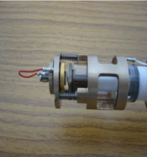
In the experiments, I used the microscope which works at both low and room temperatures. The microscope is shown in figure 2.5. In figure 2.6 the head of the microscope is shown. The head is the place where the sample and the sensor are mounted. There is a jacket to guard the piezotube and decrease the noise. In figure 2.7 the jacket is removed.
Figure 2.6: The head of the microscope where sensor is mounted.There is a steel jacket to guard the piezoelectric tube and decrease the external noise.
2.2.3
The Experiment
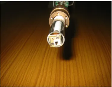
First of all, we remove the protection and mount the Hall sensor to the head by two screws. New Hall microscopes have guiding pins on the head, so that we can mount the probe on the right way for electrical connections. Mounted sensor is shown figures 2.8 and 2.9.
Then, we have to prepare the puck and place the sample on it. It is better to clean the puck with aceton. The inside of the puck must be clean. Then, we clean the sample holder and mount the sample on it with silver paint. The sample must be cleaned with dry air and if possible with aceton. Because we are approaching to the sample by using the tunnelling current between tip and the sample, the sample must be conductive. Up to 2 MΩ resistance is ok because when compared to the tip-sample resistance, it is small enough. The resistance of the sample IrMn and CoFe thin film I used in the experiments is 1.3 MΩ. Silver paint is used for sticking the sample to the holder and making a connection between the sample and the holder. It is a must because the microscope applies the bias voltage to the holder and the upside of the sample where we will image the magnetic field, must be connected to the holder again with silver paint. The sample which is connected to the holder is shown in figure 2.10.
CHAPTER 2. SCANNING HALL PROBE MICROSCOPY 13
Figure 2.7: The head of the microscope where sensor and sample are mounted. The jacket is removed in this figure.
inside the puck. We have to be careful at this stage because the surface of the sample must be clean and we shouldn’t touch it. The puck is shown in figure 2.11.
There are 3 screws on the puck for the alignment of the Hall sensor as shown in figure 2.7. After placing the puck on the head of the microscope, we have to check how well it moves on the quartz. At this stage, we have to make the sensor and the sample parallel using an optical microscope. Afterwards, we have to adjust a tilt angle about 1.5◦ between the sample and the sensor.
Then, we screw the jacket again and we are ready for scanning. The approach is done by slider piezoelectric tube. On the software we choose a tunnelling current. The software tries to approach to the sample until it reads out the same tunnelling current we have chosen. We tried to do the experiment with 1 nA. If we chose higher tunnelling current, the software gives higher voltages to the slider piezoelectric tube and it takes less time to approach. There are two piezoelectric tubes. Slider piezoelectric tube is used for approaching. The software applies a voltage to the slider piezoelectric by checking the tunnelling feedback. Slider piezoelectric moves due to this voltage. The quartz where the puck is placed
Figure 2.8: The Hall sensor mounted on the head.The quartz tube is also seen in the figure. The quartz tube is mounted on the slider piezoelectric.
moves because it is mounted to the slider piezoelectric. Then, the puck moves mechanically on the quartz and the sample approaches the sensor. To find the tunnelling, the sample moves one step forward of 2.4 µm. At this point, software applies voltage(∼ 4V) to the piezo and it approaches gradually to the sample. If it doesn’t find the specific tunnelling current; by applying negative voltage, it pulls the away from the sensor gradually again back to its step position. Then it makes the sample one step of forward (2.4 µm). It again approaches slowly in this step range to find the tunnelling. This process goes on until we read out the specified tunnelling current. When the software reads out the same tunnelling current we chose, it stops the approach. Then, we are ready to scan.
Scan is done with the scanner piezoelectric. We can assume that the sample surface is an x-y plane. We can chose the scan area and resolution before scanning. For example, the scan area is 52 µm x 52 µm and the resolution is 128 x 128 pixel. Then, the software reads out a data at each pixel and divides 52 µm2 area into
128 x 128 matrix. First it reads out data on the first line along x-axis. Then the sensor goes backward on the same line and comes to the starting point and then it moves to the next step on the y axis and continues the same way. By this way, we can also compare the data along backward and forward scanning. They must be mirror image of each other for good images. The software allows us to
CHAPTER 2. SCANNING HALL PROBE MICROSCOPY 15
Figure 2.9: The Hall sensor is mounted on the head.
scan the surface slow or fast. For fast scanning it is better to lift off the sample from the sensor. During the fast scan if there is problem like dust on the surface, sensor may crash to sample. Lift off is necessary for that reason. The real time scanning (much slower, 1 frame/second) gives better resolution because we image the sample in the tunnelling region without any lift off[15].
The Hall current that is applied to sensor may change. For GaAs Hall sensors fabricated this range is 0-5 µA. For InAs sensors it is up to 100 µA. We can decide it by measuring the resistances on the sensor. For GaAs case it is around 50 kΩ and for the InAs case, it is 6 kΩ. If the resistance is low we can apply high Hall current.
Figure 2.10: The sample mounted to the holder with silver paint is placed on tweezers. On the left part of the sample an electrical connection between top of the sample and the holder is done with silver paint.
Figure 2.11: The Hall sensor is mounted on the head.
Figure 2.12: On the right is the Hall sensor and on the left is the sample. There must be a tilt angle of 1.5◦.
Chapter 3
Hall Sensor Fabrication
Hall sensor fabrication is done in Class-100 clean room of Bilkent University Advanced Research Laboratory using photolithography techniques. Karl-Zuss MJB3 mask aligner, Thermal Evaporation coating, Reactive-Ion Etching and Rapid Thermal Annealing systems are used during the fabrication process. There are five production steps in Hall sensor fabrication. These are:
1. Hall Probe Etch 2. Mesa Etch 3. Recess Etch
4. Ohmic Contact Metallization 5. Tip Metallization
sitive chemical substance. When it is exposed with enough energy, the chemical bonds weaken and the developer of the photoresist solves the exposed parts. The photoresist we use in the class-100 clean room is AZ 5214 image reversal pho-toresist. Before exposing UV light onto the photoresist, we spin the photoresist using a spinner(fig 3.7). Different spin speeds results in different resist thicknesses (table 3.1). The advantage of spinning is that it smooths the resist on the wafer and make it uniformly spread on the surface. Although resist earns its name from its resistance to etchants, the thickness of the resist plays an important role in the etching process. Lower spin speed is favorable if we etch the wafer for long time periods after development. However the resist must be thin for getting small features(∼ 1 µm.) after development, so spin speed must be high. For Hall definition, we spin the photoresist with the maximum speed 10000 rpm to get features of size ≤ 1 µm. After spinning we prebake the sample at 110◦C for 55
seconds. Then, we do the exposure. The developer of the photoresist is AZ 400 K developer. Development time depends on the feature size (design of the mask) and the exposure time. The photoresist is image reversal. For getting reverse image of the mask we use, first we spin the resist again. After that, we bake in at 110◦C for 55 seconds on a hot plate as usual. Then, we expose UV light using a
mask. Then we bake the resist again but this time at 120◦C for 2 minutes. Next
step is very crucial. We expose without any mask and the total exposure energy (the first exposure with mask + exposure without mask) should be lower than 200 mJ/cm2. The developer(AZ 400K) is mixed with deionized water by 1 to 4
ratio and then it is used in the developing process. Photoresist sometimes sticks to the surface(eg. mask) and cannot be removed with acetone. At this time, we
CHAPTER 3. HALL SENSOR FABRICATION 19
spin speed(rpm) 2000 3000 4000 5000 6000 7000 8000 9000 Film Thickness(µm) 1.98 1.62 1.40 1.25 1.14 1.05 0.99 0.93
Table 3.1: Photoresist thickness(µm) at various spin rates(rpm). can use AZ 100 remover to get rid of photoresist.
One side of the mask is chromium and the other side is quartz. The Cr side must face the wafer during exposure. The quality of the mask depends on the size of the structures on it. Small features shows the quality of the mask.
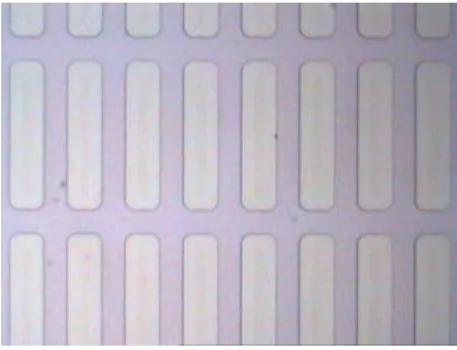
In the figures the positive and negative usage of the resist is shown. In figure 3.1, a 5 µm x 20 µm rectangular STM grating is shown. First rectangle definitions are done with photolithography and then parts between the rectangles are etched and after removing the resist, it is coated with gold. In figure 3.2, a magnetic grating fabricated using the same mask is shown. First rectangle definitions are done with photolithography as in the previous case. After development, the sample is coated with NiFe. After the lift off process, resist is removed and the parts between rectangles are NiFe and there is nothing on the rectangles. After that whole sample is coated with a thin layer of gold for electrical conductance. In figures 3.1 and 3.2 positive resist is used. In figure 3.3, the image reversal photolithography is done and sample is coated with NiFe and gold as in the previous case. Comparing figures 3.2 and 3.3, with the same mask one is positive and the other is negative photolithography.
Figure 3.3: NiFe grating.The rectangles of 5 µm x 20µm are covered with NiFe. 3.1.1.2 Mask Aligner
The Mask aligner is Karl-Zuss MJB3 mask aligner. It uses mercury lamp as UV source. The major lines in the Hg spectrum are:
- e line:546 nm - g line:436 nm - h line:405 nm - i line:356 nm
Our mask aligner uses h line. There is a time scale for deciding exposure time on the mask aligner. By multiplying power of the Hg lamp with the exposure time, we can calculate energy transferred to photresist per cm2. The mask aligner
CHAPTER 3. HALL SENSOR FABRICATION 21
Figure 3.4: Equtriangular grating of one side 10 µm.
Figure 3.5: Square grating of one side 5 µm.
proximity printing mode, the mask is placed in a close proximity to the sample. For better resolution of the features, contact printing is preferable. This technique has the capability of defining geometries of 1 µm. The only problem is that mask is deformed faster because of the actual contact between wafer and the mask. The resist sticks to the surface of the mask frequently in this mode.
3.1.1.3 Etching
There are two types of etching: Wet Etching and Dry Etching.
Wet etching is done using acidic solutions. The ones we use are H2SO4 and
Figure 3.6: Hexagonal grating of one side 10 µm.
Figure 3.7: The spinor and hot plate system.
etchants operate by first oxidizing the surface then dissolving the oxide and re-moving some of the gallium and arsenic atoms [17]. In H2SO4 solution, H2SO4
is mixed with H2O2 and H2O. Here H2O2 is the oxidizing agent, H2SO4 dissolves
the oxide and remove GaAs. In Hall Probe Etch , H2SO4 solution is used. The
etch rate is on the order of 2-2.5 nm/second. In Mesa Etch step, we again use the same solution. Here the concentration of H2SO4 increases tremendously by
lowering the deionized water concentration. The typical etch rate for this solu-tion is 0.8 µm/minute. The HCl solusolu-tion is used in Recess Etch of the GaAs processing. In the solution, HCl, H2O2, H2O are used. This solution etches 50
µm/hour. In wet etching, etchant solution usually etches from the side walls of the resist. This property is named undercut. Due to undercut, we cannot get features having perpendicular side walls. If we are trying to get features of one
CHAPTER 3. HALL SENSOR FABRICATION 23
Figure 3.8: Karl-Zuss MJB3Mask aligner. Oxygen Plasma Hall Definition Etch Flow Rate 20 sccm. 20 sccm. Base Pressure 8 10−3 4 10−3
Power 50 W. 75 W. Duration 5 min.
Table 3.2: Typical Oxygen Plasma Etching and Hall Probe Definition Etching settings. Hall Probe etch rate is 400-500 ˚A/minute.
micron size (like in the case of Hall etch), letting the sample in acidic solution too long can harm the features because of undercut. Most of the wet etchants have anisotropic behavior. They etch in one direction faster than the other. This can be understood from the interatomic bonds. Some bonds are weaker and on those planes wet etchants etch faster.
The other way is dry etching. Dry etching is done by Plasma Etching, Reac-tive Ion Etching(RIE), Ion Milling methods. Dry etching has some advantages over wet etching. Lateral etch rate is nearly zero, so undercutting doesn’t occur. Because of that reason, smaller patterns can be fabricated. Etch rate is more controllable. Plasma Etching is usually done for cleaning the sample from pho-toresist or other chemicals that sticks on the surface. I tried Oxygen Plasma for a number of times for cleaning the photoresist from the wafer. In Ion milling,
the wafer. Figure 3.10 shows the RIE chamber during the ionization process.
Figure 3.9: Chamber of the RIE system.
Figure 3.10: Chamber of the RIE system. Ions bombard the surface of the wafer.
3.1.1.4 Metallization
The purpose of the metallization is to make electrical connections onto the device. Most of the time, ohmic contact is necessary for allowing current to flow into the device. For n-type GaAs Gold-Germanium based metallization is necessary. For the GaAs sensors 270 ˚A Ge and 540 ˚A Au are coated on the surface. Using Rapid
CHAPTER 3. HALL SENSOR FABRICATION 25
Thermal Annealing at 450◦C, Ge dopes the GaAs during alloy. Ge and Au moves
into the surface of the wafer and electrical conduction is guaranteed [17]. Ge-Au is usually applied with another metal such as nickel or silver. The thickness of this layer could be 60 ˚A. Ni behaves like a wetting agent and prevent GeAu metal from balling up during annealing process. It is better to coat 100 ˚A Ti and 1500 ˚
A Au layer after annealing process. Ti helps Au stick to the surface and this last layer serves for easy bonding of the sensor the chip holder.
3.2
Wafer
In Hall sensor fabrication, I used two different kinds of wafers. First of them is GaAs/Al0.3Ga0.7As heterostructure sent by Dr. Hadas Shtrikman. These kind
of Hall sensors are usually used for low temperature measurements. The lattice constants of GaAs and Al0.3Ga0.7As are similar and the whole structure can be
treated like a single crystal. In the GaAs/Al0.3Ga0.7As heterostructure the top
layer is GaAs. Then, there comes the doped AlxGa1−xAs layer. There is a spacer
layer of undoped AlxGa1−xAs layer between GaAs and AlxGa1−xAs layers. In the
V-shaped potential at the interface undoped AlxGa1−xAs and GaAs, electrons are
trapped. The layer thickness where electrons are trapped is 10-20 nm and it lies 50-60 nm below surface of the wafer[2]. Because of that reason, at the Hall probe definition step, the etch depth should be at least 50 nm. It is better to etch down to 100-120 nm to guarantee a good Hall definition. The thin layer (10 nm) is also preferable because field distribution is sampled at a well defined height.
Hall sensors made from InSb wafers are shown to give good results for room temperature application[2]. Instead, I fabricated InAs sensors for room temper-ature experiments. The layers of InAs wafers are shown in the table below. The wafer was sent by Dr. Brian Bennet from Naval Research Lab., in the USA.
Bennett from Naval Research Lab, USA.
3.2.1
Wafer Cleaning
Before beginning to the process wafer must be clean as much as possible. For Hall sensor production, wafer is cleaved into 5 mm to 5 mm squares with a steel scriber. During this process, some small particles broken from the wafer may scratch or stick to the surface. If the wafer seems to be clean under optical microscope, just letting the wafer wait in acetone for two minutes, then, in isopropilalcohol for two minutes and repeating it for three times is enough. After that, we have to make sure that it is dry by blowing with nitrogen gun. It is usually better to clean the wafer in acetone beaker in ultrasonic bath. By this way, we can easily get rid of the things stuck onto the surface. The conventional way to clean the wafers is named three solvent cleaning.Its steps are:
• Keeping in boiling trichloroethane(methyl chloroform) for two minutes. • Keeping in acetone for five minutes.
• Keeping in boiling isopropilalcohol for three minutes
CHAPTER 3. HALL SENSOR FABRICATION 27
3.3
Fabrication
3.3.1
Hall Probe Definition
The most critical step in Hall sensor production is Hall probe definition. After cleaning the wafer (5mm x 5mm), we spin the resist 2 seconds at 1300 rpm and 40 seconds at 10000 rpm. Because feature size 1 µm, spinning with high speed is important. After prebake of 55 seconds at 1100C, we expose for 30 seconds develop
for 20 seconds. We fabricate 4 sensor at a time. The development time depends on how old the resist and the developer are. It is better to see the development of the resist with naked eye instead of waiting for 20 seconds. If we overdevelop it, we have to clean the resist and start from the beginning. Over development of small features is very dangerous because of undercutting. Then, we etch the wafer. The solution is H2SO4:H2O2:H2O. The typical etch rate for GaAs is 2
nm/second.Then we clean the sample with acetone and isopropilalcohol.
For the InAs wafers, the etch depth was more mysterious. The active layer seems to at 380 ˚A below the surface. From past experince with the GaAs wafers, we know that the resistances between two ends of the hall cross is nearly 50 kΩ. The tip and the Hall sensor resistance should be larger than 25 MΩ for preventing any leakage in the tunneling current. For a high tip resistance, the hall etch depth appeared to more than 2 µm. The etch is done using RIE, after postbaking the resist at 1200C for two minutes. Development process may also harm the wafer
structure. AZ 400 K etches the surface of the InAs wafer. If we face a problem after development, we don’t have any chance to clean the resist and start from the beginning.
3.3.2
Mesa Etch
On one wafer, 4 Hall definitions are made. Mesa etch is for separating these four probes from each other. I spin the resist 2 seconds at 1300 rpm and 40 seconds at 7000 rpm. After prebake, I exposure it for 30 seconds. The development
Figure 3.12: Hall probe definition on InAs wafer. Typical size of the hall sensor 1 µm. Etch depth is more than 2.5 µm.
time is 45 seconds. Then, we etch in the solution of H2SO4,H2O2,H2O. Typical
etch depth should be 1-1.5 µm. The etch duration of one and a half minute is satisfactory.
For the InAs sample, we already etched more than 2 µm. We can safely skip this step.
3.3.3
Recess Etch
After fabrication, the electrical connections are made using bonding wire. Bond-ing wires should be stuck to the recess etched parts. The process steps till etchBond-ing is similar to Mesa etch. Before etching we have to make sure that the edges of the wafer is clean. We can clean the undeveloped parts using acetone. The etching solution is HCl,H2O2,H2O. The recess etch depth is determined by the diameter
CHAPTER 3. HALL SENSOR FABRICATION 29
of the bonding wire. Up to now, we used two kinds of gold wires with diameters 12 µm and 25 µm. For that reason, it is safer to do the recess etch more than 50 µm.
Figure 3.13: The Recess Etch.
3.3.4
Ohmic Contact Metallization
Ohmic contact Metallization is very important in Hall sensors of GaAs wafer. The process is similar to the previous ones. First spin the resist at 1300 rpm for 2 seconds and 6000 rpm for 40 seconds. Then Prebake at 1100C for 55 seconds.
Expose for 1 minute. Before Development we have to let it wait in chlorobenzol for one minute. What cholorobenzol does is that it makes the upper part of the photoresist harder. In the lift off process, it makes acetone etch from the side walls of the resist and remove the resist part easily. We may wait 10 minutes for drying after letting it wait in cholorobenzol. Then, develop for 45 seconds. Ohmic contact metallization is 270 ˚A Ge, 540 ˚A Au, 60 ˚A Ni as discussed previously. After metallization, lift off process is done in an acetone beaker. We can change the power of the ultrasonics bath with a variac. Using ultrasonic bath with low power sometimes help the lift off process. For InAs case, the resistances of the Hall probe were around 6-8 kΩ. This resistance is low with respect to GaAs case. We didn’t do any ohmic contact metallization and coated with 100 ˚A Ti 1500 ˚A Au only.
After lift-off rapid thermal annealing is done at 4500C for 45 seconds. After
that, we do the same process from the beginning, but this time we coat with 100 ˚
A Ti 1500 ˚A Au for easy bonding.
3.3.5
Tip Metallization
The last step is tip metallization. The process part is just the same as ohmic contact metallization except we use tip mask in this process. We coat with 100 ˚
A Ti 500 ˚A Au. This metallization aims the high conductivity along the tip and easy approach to the sample before scanning process.
Figure 3.15: In the figure the gold coated tip is shown near the hall sensor. Before starting with a Hall sensor, testing the microscope with a STM tip and a grating is usually better. For this purpose various gratings with different
CHAPTER 3. HALL SENSOR FABRICATION 31
using discussions of the previous chapter. We have to do noise analysis to decide the range of the applicable Hall current[18].
The main noise that determines the maximum Hall current that can be applied is Johnson Noise. Johnson noise is:
Vj =
q
4kbT RBW (4.1)
where kb is the famous Boltzmann constant, T is the temperature, R is the
series resistance of the sensor and BW is the measurement bandwidth. In GaAs sensors the series resistance is around 50kΩ. In InAs sensors, it is around 6kΩ at 300 K. The high self resistance in GaAs sensors increases this thermal noise tremendously. The Hall voltage is given as:
VH = IHRHB (4.2)
where VH is the Hall voltage IH is the applied Hall current RH is the Hall
CHAPTER 4. NOISE ANALYSIS 33
coefficient B is the magnetic field. Then signal to noise ratio [18] is:
S N = IHRHB √ 4kbT RBW (4.3)
The increase in the signal to noise ratio decreases the minimum detectable magnetic field. When signal to noise ration is 1, we get the minimum detectable magnetic field [19] [7]. 1 = S N = IHRHB √ 4kbT RBW (4.4) Bmin = √ 4kbT RBW IHRH (4.5) Bmin = Vnoise IHRH (4.6) The noise analysis of the InAs and GaAs sensors are done at both 77 K and at 300 K. In this process, the hall voltage is connected to the sound card of a pc. and a fast Fourier transform signal analyzer is used for detecting the noise. The signal analyzer gave us the dB values at the output of the Hall voltage for different applied Hall currents as a function of frequency. The noise at the Hall voltage is calculated by:
dB = clog(Vnoise Vref
) (4.7)
Vref is the reference voltage on the sound card and c is a constant. This
voltage and the constant is calculated by applying different known signals to the sound card by using a signal generator.
Figure 4.1: Vref(in mV) of the sound card at low frequencies.
All these noise measurements are done when there is no external field with the sampling rate of 1 Hz. Magnetic field is calculated according to
B = V IHRHG
(4.9) where G is the gain of the Hall amplifier of the electronics which is set as 100100.
The noise data is taken 20 times for each sampling. The averaged noise spec-trum is used in the calculations afterwards. The city electricity has a frequency of 50 Hz. Because of that reason, the noise at the frequencies of 50 Hz. and multiples of 50 Hz are filtered.
Chapter 5
Noise Analysis of GaAs Sensors
5.1
Measurement of Hall Coefficient
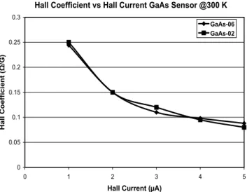
Two properly working Hall sensors are chosen for this experiment. Hall coeffi-cients are calculated at both 77 K and 300 K for two different GaAs Hall sensors. In figure 5.1 room temperature Hall coefficient calculations are shown. From the figure, it is clear that at low currents (1µA) the Hall coefficient is at the highest value. For a well fabricated GaAs sensor, this value is usually higher than 0.2 Ω/G. As the Hall current increases the coefficient decreases below 0.1 Ω/G. In figure 5.2, the same calculation is shown for 77 K. From the figure, it is shown that Hall coefficients increase slightly at low temperature. One important remark for Hall coefficient calculation is that, by changing the direction of the current sometimes we do not get the same Hall coefficient for a fixed applied current. That means that Hall sensors sometimes work better for one direction of the Hall current. The ideal sensor don’t have this kind of property, so another way of deciding which probe is better fabricated, is looking at hall coefficients for fixed value of Hall currents applied in the reverse directions. The Hall coefficients calculated are in good agreement with the previously fabricated GaAs sensors.
Figure 5.1: The Hall coefficient calculation of two GaAs sensors at room temper-ature for different Hall currents.
5.2
Noise Measurement of GaAs Hall Sensors
The noise spectrums of arbitrary chosen GaAs Hall probes are measured at 77 K and 300 K. Their spectrum are in good agreement with each other. The room temperature noise spectrum of GaAs sensors is also compared with the previously published noise analysis of GaAs sensors.
5.2.1
Room Temperature Measurements at 300 K
The Hall current that could be applied is up to 5 µA for room temperature applications. Further increasing the current can damage the sensor. It is most easily seen from the distortions of the BH curves at high Hall current. During the testing of the sensor, I also saw GaAs sensors to which 8 µA is applicable and it is the highest level of Hall current for my Hall sensors.
In figures 5.3, 5.4, 5.5, 5.6, 5.7 the measured noise spectrum of GaAs sensors is shown. Previously, noise spectrum of GaAs sensors is also analyzed (fig 5.8)[7]. In this paper(figure 5.8) the typical noise is around 100 mG/Hz1/2 which is in
CHAPTER 5. NOISE ANALYSIS OF GAAS SENSORS 37
Figure 5.2: The Hall coefficient calculation of two GaAs sensors at 77 K for different Hall currents.
good agreement with our results.
The other thing that can be calculated is the minimum detectable field as a function Hall current for different frequencies. The graph of minimum detectable field for GaAs wafer from the same publication is shown in figure 5.9. In the graph, it is shown that minimum detectable field is slightly larger that 100 mG/Hz1/2for
three different frequencies(250, 500, 1000 Hz). For newly fabricated Hall sensors, this field is again similar as shown in figure 5.10.
5.2.2
Low Temperature Measurements at 77 K
For low temperature measurement, I applied Hall current up to 20µA, more current could damage the sensor. The resistances of the GaAs sensor drop to 3-4 kΩ range at 77 K. When the sensor is cooled down fast, the free carriers can freeze. It is better to use an infrared LED to to make the sensor work properly. The infrared LED can falsify the measurement if it is on during the measurement. In the graphs 5.12,5.13,5.14,5.15, the noise measurement of GaAs sensors are shown for 5,10,15,20 A. From the figures, it is clear that noise nearly falls of to one tenth of its value at room temperature. This is mostly because of the series resistance
Figure 5.3: Noise measurement for 1 µA Hall current of GaAs sensor (no2) at 300 K.
of the sensor discussed in the previous chapter. Minimum detectable field as a function of applied current is also shown in figure 5.11.
CHAPTER 5. NOISE ANALYSIS OF GAAS SENSORS 39
Figure 5.4: Noise measurement for 2 µA Hall current of GaAs sensor (no2) at 300 K.
Figure 5.5: Noise measurement for 3 µA Hall current of GaAs sensor (no2) at 300 K.
Figure 5.6: Noise measurement for 4 µ A Hall current of GaAs sensor (no2)at 300 K.
Figure 5.7: Noise measurement for 5 µ A Hall current of GaAs sensor (no2) at 300 K.
CHAPTER 5. NOISE ANALYSIS OF GAAS SENSORS 41
Figure 5.8: Noise measurement for 2.5 µA Hall current at room temperature from a publication [7].
Figure 5.9: Previously measured minimum detectable field as a function of Hall current from a publication is shown [7].
Figure 5.10: Minimum detectable field of GaAs Hall sensor(no2) as a function of Hall Current at 300 K.
Figure 5.11: Minimum detectable field of GaAs Hall sensor (no2) as a function of Hall Current at 77 K.
CHAPTER 5. NOISE ANALYSIS OF GAAS SENSORS 43
Figure 5.12: Noise measurement for 5 µA Hall current of GaAs Hall sensor (no2) at 77 K.
Figure 5.13: Noise measurement for 10 µA Hall current of GaAs Hall sensor (no2) at 77 K.
Figure 5.14: Noise measurement for 15 µA Hall current of GaAs Hall sensor (no2) at 77 K.
Figure 5.15: Noise measurement for 20 µA Hall current of GaAs Hall sensor (no2) at 77 K.
Chapter 6
Noise Analysis of InAs Sensors
6.1
Measurement of Hall Coefficient
Two properly working sensors were chosen from fabricated InAs sensors as done in the GaAs case. First Hall coefficient measurements are done. In these mea-surements, InAs sensors proved to be working properly up to 100 µA Hall current. Because of that reason, the assumption before noise analysis was that they would be more suitable for room temperature applications. However to be on the safe side, Hall current up to 50 µA is used during noise analysis .
In the figures 6.1,6.2,6.3 the Hall coefficient calculations are shown. There are two important results from these graphs. First of them, is after 10-20 µA range the Hall coefficient decreases tremendously.The other is that up to 10 µA the hall coefficient is similar to the GaAs sensors.
6.2
Noise Measurement of InAs Hall Sensors
The noise spectrum is analyzed as discussed in chapter 4 for 77 K and 300 K.
6 0.033 0.034 7 0.03 0.03 8 0.027 0.027 9 0.025 0.025 10 0.023 0.023 11 0.022 0.021 12 0.021 0.02 13 0.019 0.018 14 0.018 0.017 15 0.17 0.17 16 0.016 0.016 17 0.016 0.016 18 0.015 0.015 19 0.015 0.015 20 0.014 0.014 25 0.013 0.009 30 0.012 0.006 40 0.01 0.004 50 0.009 0.003 60 0.009 0.002 70 0.009 0.002 80 0.008 0.002 90 0.008 0.002 100 0.007 0.001
Table 6.1: Measured Hall Coefficient values for two different InAs sensors at room temperature for various applied current.
CHAPTER 6. NOISE ANALYSIS OF INAS SENSORS 47
Figure 6.1: The Hall coefficient calculation of two InAs sensors at room temper-ature for different Hall currents.
6.2.1
Room Temperature Measurements at 300 K
At the room temperature, InAs is shown to be much better than the GaAs sensors. The noise is much lower than 100 mG/Hz1/2 between 10-20 mG/Hz1/2. It can be
clearly seen from figures 6.4-6.9. In this figures different Hall currents are applied and the noise spectrum is analyzed.
In figure 6.11 the minimum detectable field is shown as a function of Hall current at room temperature.
6.2.2
Low Temperature Measurements at 77 K
At 77 K, the noise of the InAs sensors decrease slightly to 10 mG/Hz1/2.
Increas-ing the current doesn’t mean much because although current is increasIncreas-ing Hall coefficient is decreasing, so the value of the magnetic field does not change much. At the 77 K, the minimum detectable field is also measured as a function of Hall current. Minimum detectable field is slightly lower than the room tempera-ture case. That is logical because the series resistance of the hall sensor drops to
Figure 6.2: The Hall coefficient calculation of two InAs sensors at 77 K for dif-ferent Hall currents.
4-5 kΩ.
As a result GaAs sensors are shown to be working much better at low tem-perature than room temtem-perature, so they are suitable for low temtem-perature mea-surements like investigations of domains in superconductors.
InAs sensors are shown to have much lower minimum detectable field than GaAs ones at room temperature. However cooling the sensor to 77 K doesn’t have tremendous effect as in the case of GaAs ones, the minimum detectable field doesn’t change much. Comparing InAs ones with widely used InSb Hall sensors for room temperature measurements, InSb ones have better quality for 300 K which is shown in the last figure of this chapter [7].
CHAPTER 6. NOISE ANALYSIS OF INAS SENSORS 49
Figure 6.3: The Hall coefficient calculation of an InAs sensors both at 77 K and at room temperature for different Hall currents.
Figure 6.4: Noise measurement InAs sensor (no4) for 5 µA Hall current at 300 K.
Figure 6.5: Noise measurement InAs sensor (no4) for 10 µA Hall current at 300 K.
Figure 6.6: Noise measurement InAs sensor (no4) for 20 µA Hall current at 300 K.
CHAPTER 6. NOISE ANALYSIS OF INAS SENSORS 51
Figure 6.7: Noise measurement InAs sensor (no4) for 30 µA Hall current at 300 K.
Figure 6.8: Noise measurement InAs sensor (no4) for 40 µA Hall current at 300 K.
Figure 6.9: Noise measurement InAs sensor (no4) for 50 µA Hall current at 300 K.
Figure 6.10: The minimum detectable magnetic field is again measured for dif-ferent Hall currents at room temperature for InAs sensor (no4).
CHAPTER 6. NOISE ANALYSIS OF INAS SENSORS 53
Figure 6.11: Noise measurement of InAs sensor (no4) for 5 µA Hall current at 77 K.
Figure 6.12: Noise measurement of InAs sensor (no4) for 10 µA Hall current at 77 K.
Figure 6.13: Noise measurement InAs sensor (no4) for 20 µA Hall current at 77 K.
Figure 6.14: Noise measurement InAs sensor (no4) for 30 µ A Hall current at 77 K.
CHAPTER 6. NOISE ANALYSIS OF INAS SENSORS 55
Figure 6.15: Noise measurement InAs sensor (no4) for 40 µA Hall current at 77 K.
Figure 6.16: Noise measurement InAs sensor (no4) for 50 µA Hall current at 77 K.
Figure 6.17: The minimum detectable magnetic field is measured for different Hall currents at 77 K for InAs sensors.
Figure 6.18: Minimum detectable magnetic field as a function of Hall current for InSb Hall sensors at 300 K [7].
Chapter 7
Conclusions and Future Work
In this thesis, Scanning Hall Probe Microscopy is discussed. First of all, the fabrication of Hall sensors from GaAs and InAs wafers using optical lithography techniques are mentioned in detail. Then, basic principles of Hall magnetometry is explained. After that the usage of the Scanning Hall Probe Microscope during an experiment is discussed. Afterwards, there comes the noise discussions of Hall sensors. Finally, the analyzed noise spectrum of both previously known GaAs and new InAs sensors are discussed.
In the publications GaAs was shown to be good at low temperature measure-ments because of its low noise at 77 K. Hall coefficients, the measured minimum detectable field values and noise spectrum for different Hall currents are mea-sured and calculated. The new results are in pretty good agreement with the previous results. The minimum detectable field is around 100 mG/Hz1/2 at room
temperature and lower than 10 mG/Hz1/2 at 77 K. The Hall coefficient does not
change much and is around 0.2 Ω/G for both 77 K and 300 K. The decrease in the noise level can be explained with the decrease from 50 kΩ to 4-5 kΩ in the series resistance at low temperature as discussed in Chapter 4 in detail. InAs sensors showed different behaviour than GaAs ones. We can apply up to 100 µA to InAs sensors both at low temperature and at low temperature. Their serial resistance doesn’t change significantly with the temperature. Their noise level decrease slightly with temperature, but we can safely say that the noise is always
with the widely used InSb sensors for room temperatures, InAs sensors show lower quality.
The carrier density of the InAs wafer was known previously. It is shown in table 3.3. A simple calculation of Hall coefficient using this carrier density gives:
RH =
1
nq = 0.019Ω/G (7.1) This result is expected by looking at the Hall coefficient measurement of InAs sensors shown in table 6.1. This is another point supporting the measurements.
The minimum detectable fields measured for GaAs and InAs are shown in table 7.1. In this table the minimum detectable field of InAs (from a publication) at room temperature is shown for comparison.
In the future, these sensors could be used for both low temperature and room temperature applications and they are promising because they are less dependent on the temperature than the other two types of sensors.
Bibliography
[1] John J. Mallinson, The Foundations of Magnetic Recording, Academic Press Inc.,102-116, 1987.
[2] S. Bending, Local Magnetic probes of superconductors, Adv. in Phys.,48(4), 1999.
[3] K.S. Novoselov, S.V. Morozov, S.V. Dubonos, M. Missous, A.O. Volkov, D.A. Christian, and A.K. Geim, Submicron probes for Hall magnetometry over the extended temperature range from helium to room temperaure, Appl. Phys. Lett.,93(12), 2003.
[4] Charles Kittel, Introduction to Solid State Physics, John Wiley and Sons Inc.,441-458, 1996.
[5] David Jiles, Introduction to Magnetism and Magnetic Materials, Chapman and Hall Inc.,48-97, 1991.
[6] Y. G. Wang, A. K. Petford Long, T. Hughes, H Laidler, K. O’Gardy, M.T Kief,Magnetisation of reversal of the ferromagnetic layer in IrMn/CoFe bi-layer films, Journal of Magnetism and Magnetic Materials, 1081-1084,2002. [7] A. Oral, M. Kaval, M. Dede, H. Masuda, A. Okamoto, I. Shibasaki, and A. Sandhu, RT-SHPM Imaging of Garnet Films Using New High Performance InSb Sensors, IEEE Trans. on Magnetics, 38(5),2002.
[8] A. Sandhu, K. Kurosawa, M. Dede, A. Oral, 50 nm Hall Sensors for Room Temperature Scanning Hall Probe Microscopy, Jpn. J. Appl. Phys.,43(2), 2004.
external magnetic field using a sub-micron GaAS SHPM,Journal of Crystal Growth 227-228, 899-905, 2001.
[13] A. Sandhu, H. Masuda, A. Oral, S. J. Bending, Direct Magnetic Imag-ing of Ferromagnetic Domain Structures by Room Temperature ScannImag-ing Hall Probe Microscopy Using a Bismuth Micro-Hall Probe, Jpn. J. Appl. Phys.,40(5B),524-527,2001.
[14] Nanomagnetics Instruments Ltd, www.nanomagnetics-ins.com.
[15] A. Sandhu, H. Masuda, A. Oral, S. J. Bending,Room Temperature Sub-Micron Magnetic Imaging by Scanning Hall Probe Microscopy, Jpn. J. Appl. Phys.,40(6B), 2001.
[16] W. S. Deforest, Photoresist Materials and Processes, McGraw and Hill Inc.,19-132, 1975.
[17] R. Williams, Modern GaAs Processing Techniques, Artech House Inc., 79-139, 1990.
[18] G. Jung, M. Ocio, Magnetic noise measurements using cross-correlated Hall sensor arrays, Appl. Phys. Lett.,78(3), 2001.
[19] G. Boerom, M. DEmierre, A. Besse, R.S. Popovic,Micro-Hall devices: perfor-mance, technologies and applications, Sensors and Actuators A, 106, 314-320, 2003.
[20] Ben G. Streetman, Solid State Electronic Devices, Prentice and Hall Inc.,89-92, 1995.
![Figure 2.3: Typical schematic of a Hall sensor for magnetic field measurement.[2]](https://thumb-eu.123doks.com/thumbv2/9libnet/5745581.115797/21.892.321.639.176.450/figure-typical-schematic-hall-sensor-magnetic-field-measurement.webp)
![Figure 2.5: Low temperature Scanning Hall Probe Microscope[14].](https://thumb-eu.123doks.com/thumbv2/9libnet/5745581.115797/24.892.295.672.497.746/figure-low-temperature-scanning-hall-probe-microscope.webp)