Journal of Physics D: Applied Physics
PAPER
Decoupling contact and mirror: an effective way to
improve the reflector for flip-chip
InGaN/GaN-based light-emitting diodes
To cite this article: Binbin Zhu et al 2016 J. Phys. D: Appl. Phys. 49 265106
View the article online for updates and enhancements.
Related content
Optimized subsequent-annealing-free Ni/Ag based metallization contact to p-type GaN for vertical light emitting diodes with high yield and extremely low operating voltage (2.75 V@350 mA, >95%)
Ting Tian, Liancheng Wang, Enqing Guo et al.
-Reducing forward bias voltage of InGaN/GaN-based light emitting diodes by using (In)GaN contact layer
Daesung Kang, Younghun Han, Donghun Kang et al.
-Insights into annealing-induced ohmic contact formation at graphene/p-GaN interface with a NiOx contact layer
S Chandramohan, Beo Deul Ryu, Tae Hoon Seo et al.
-Recent citations
On the Hole Injection for III-Nitride Based Deep Ultraviolet Light-Emitting Diodes
Luping Li et al
-Enhanced light extraction efficiency of a InGaN/GaN micro-square array light-emitting diode chip
Dan Han et al
-High-luminous efficacy white light-emitting diodes with thin-film flip-chip technology and surface roughening scheme
Xiao-Long Hu et al
1. Introduction
High-power InGaN/GaN-based LEDs have shown great potential to replace traditional lighting techniques and can be used in many lighting aspects, such as traffic light, indoor or outdoor lighting and LCD backlight [1]. However, the light extraction efficiency is still one of the most critical obstacles which prevents further improvement of the LED efficiency [2, 3]. For flip-chip LEDs, the reflector on p-GaN is essential to
improve the light extraction efficiency since light is reflected by the mirror and emitted out from the backside of LEDs [4, 5]. There are many options of metal combinations for the contact mirror, such as Ni/Ag/Pt [3], Ni/Ag/Ti/Au [5], Ni/Au/W/Ag [6] and Ni/Ag/Ru/Au [7]. In these metal stacks, the first layer next to the p-GaN is always Ni which is critical to form ohmic contact [8–10]. The second layer is usually a highly reflective metal such as Ag or Au [11], while Ag is preferable due to its higher reflectivity. In the conventional
Journal of Physics D: Applied Physics
Decoupling contact and mirror: an effective
way to improve the reflector for flip-chip
InGaN/GaN-based light-emitting diodes
Binbin Zhu1,2, Wei Liu1, Shunpeng Lu1, Yiping Zhang1, Namig Hasanov1,Xueliang Zhang1, Yun Ji1, Zi-Hui Zhang1, Swee Tiam Tan1, Hongfei Liu3 and Hilmi Volkan Demir1,2,4
1 Luminous! Centre of Excellence for Semiconductor Lighting and Displays, The Photonics Institute.
School of Electrical and Electronic Engineering, Nanyang Technological University, 50 Nanyang Avenue, Singapore 639798, Singapore
2 School of Physics and Mathematical Sciences, Nanyang Technological University, 21 Nanyang Link,
Singapore 637371, Singapore
3 Institute of Materials Research and Engineering, Agency of Science, Technology and Research,
Singapore 117602, Singapore
4 Department of Physics, UNAM-Institute of Material Science and Nanotechnology, Bilkent University,
Ankara TR-06800, Turkey
E-mail: [email protected]
Received 22 March 2016, revised 29 April 2016 Accepted for publication 5 May 2016
Published 26 May 2016
Abstract
In the conventional fabrication process of the widely-adopted Ni/Ag/Ti/Au reflector for InGaN/GaN-based flip-chip light-emitting diodes (LEDs), the contact and the mirror are entangled together with contrary processing conditions which set constraints to the device performance severely. Here we first report the concept and its effectiveness of decoupling the contact formation and the mirror construction. The ohmic contact is first formed by depositing and annealing an extremely thin layer of Ni/Ag on top of p-GaN. The mirror construction is then carried out by depositing thick layer of Ag/Ti/Au without any annealing. Compared with the conventional fabrication method of the reflector, by which the whole stack of Ni/Ag/Ti/Au is deposited and annealed together, the optical output power is improved by more than 70% at 350 mA without compromising the electrical performance. The mechanism of decoupling the contact and the mirror is analyzed with the assistance of contactless sheet resistance measurement and secondary ion mass spectrometry (SIMS) depth profile analysis. Keywords: decoupled, ohmic contact, mirror, light-emitting diodes
(Some figures may appear in colour only in the online journal) B Zhu et al Printed in the UK 265106 JPAPBE © 2016 IOP Publishing Ltd 2016 49
J. Phys. D: Appl. Phys.
JPD
0022-3727
10.1088/0022-3727/49/26/265106
Paper
26
Journal of Physics D: Applied Physics IOP
doi:10.1088/0022-3727/49/26/265106 J. Phys. D: Appl. Phys. 49 (2016) 265106 (6pp)
B Zhu et al
2
flip-chip fabrication process, the whole reflector metal stack is usually deposited onto the p-GaN. In order to facilitate the formation of ohmic contact, a subsequent high temperature annealing in oxygen ambient is necessary. However, annealing at high temperature will severely decrease the reflectivity of the mirror due to Ag agglomeration and Ag intermixing with other metals [5, 12]. These issues have considerably reduced the performance of the LED devices. A two-step deposition method has been reported [5] to solve the problem of Ag inter-mixing with Au in the Ni/Ag/Au reflector where the Ni/Ag layer was deposited and annealed first, followed by the Au layer deposition without further annealing. Although the Ag intermixing issue has been addressed, the Ag agglomeration issue still persists since the whole Ag layer has gone through the annealing process. The reflectance of the reflector in the work was below 90% at 450 nm, which needs to be further improved for high performance LEDs.
In this work, we propose the concept of decoupling the contact and the mirror in the reflector fabrication process for the first time. The contact composed of an extremely thin Ni/Ag layer is deposited and annealed. Then the mirror composed of thick Ag/Ti/Au layer is formed without any annealing. The Ag layer in the contact is so thin that it will not cause the agglomeration problem while it is sufficient for the ohmic contact formation together with Ni. The thick Ag layer in the mirror remains intact with high reflectivity since it is not subject to high temperature process. The reflectance of the proposed reflector can reach 95% at 450 nm and the optical output power of the blue LEDs fabricated with the proposed method has been improved by more than 70% compared to that of the LEDs fabricated with the conventional method at 350 mA. The mechanism of decoupling the contact and the mirror has been investigated in details through contactless sheet resistance measurement and secondary ion mass spec-trometry (SIMS) analysis.
2. Experiment
The samples used in the work were grown on c-plane sap-phire substrates in a metal-organic chemical vapor deposition (MOCVD) system. A GaN nucleation layer was grown on the substrate first, followed by an unintentionally doped GaN as the buffer layer. Then, a silicon doped n-GaN layer was grown on top of the buffer layer. Next, eight pairs of InGaN/ GaN multiple quantum wells were grown as the active region. After that, a p-type Al0.2Ga0.8N layer was grown as the
elec-tron blocking layer (EBL). Finally a p-type doped GaN layer was grown on top of the EBL. Details of the growth para-meters can be found in the related reference [13]. The as-grown wafers were fabricated into LED chips by a standard fabrication process. As a reference, the conventional Ni/Ag/ Ti/Au (1 nm/150 nm/100 nm/65 nm) reflector was deposited by an electron beam evaporator and then annealed at 500 °C in N2:O2 (4:1) atmosphere for 5 mins. For the proposed reflector,
the contact layer composed of a thin Ni (1 nm)/Ag (X nm) was firstly deposited on the p-GaN surface and annealed in
the same condition as the reference. Here X equals to 0, 1, 3 and 5. Then, the mirror composed of Ag/Ti/Au (150 − X nm/100 nm/65 nm) layer was deposited and no more annealing process was conducted for the mirror layer. Scanning electron microscope (SEM) (JEOL JSM-5600LV) was used to examine the surface morphology of the samples. Reflectivity was mea-sured by UV/Vis/NIR Spectrophotometer System (PerkinElmer Lambda 950). The current–voltage (I–V ) characteristics of the LED chips was measured using a LED quick tester (M2442S-9A Quatek Group) and the optical output power was measured by Ocean Optics spectrometry (QE65000), which was attached to an integrating sphere. The sheet resistance of the thin Ni/Ag contact layers before and after annealing was measured with a four-probe contactless sheet resistance measurement system. Time-of-flight secondary ion mass spectroscopy (ToF-SIMS) was used to analyze the depth profile of the metal stack. 3. Results and discussion
The contact layer composed of various thin Ni/Ag bilayers has been studied using SEM to find out the optimal Ag thick-ness as shown in figure 1. An ideal contact should have low contact resistance and turn-on voltage, and should also have a smooth surface morphology. In figures 1(a)–(d), the sur-face morphologies of the contact layers with Ag thickness of 0, 1, 3, and 5 nm after annealing are compared and it can be seen that the original smooth surface becomes roughened with the occurrence of cluster structures and the density of cluster structures increase as the Ag thickness increases. The cluster structures are due to Ag agglomeration caused by the annealing process. Obviously, the Ag agglomeration depends on the Ag thickness. For the sample without Ag deposition in the contact layer as shown in figure 1(a), the surface is very flat and smooth. It has been reported that Ni can form nano-clusters after annealing [14]. In our case, the thickness of Ni, which is 1 nm may be too thin to form clusters after annealing or the size of the clusters is too small to be observed in SEM imaging. According to the surface morphologies shown in figure 1 the optimal Ag thickness for the contact layer is 1 nm which presents least Ag agglomeration. The Ni only contact forms only Schottky contact with p-GaN though its surface morphology looks smoother. The electrical properties of the various contact layers will be examined later.
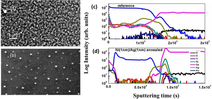
After the formation of the contact layer, the mirror com-posed of thick Ag/Ti/Au is constructed on top of the contact. The surface morphology of the proposed reflector composed of the decoupled contact and mirror is shown in figure 2(b), along with that of the reflector built with the conventional method in figure 2(a) for comparison. As usual, the conven-tional Ni/Ag/Ti/Au reflector suffers a severe degradation on the surface morphology featured by the large number of clus-ters and the roughened surface as shown in figure 2(a). On the contrary, with the decoupling of the contact and the mirror the surface morphology is greatly improved which exhibits much smoother surface and significantly reduced cluster structures both in density and size. SIMS depth analysis has also been
applied for the two reflectors to examine the element distribu-tion as shown in figures 2(c) and (d). In figure 2(c) for the reference sample, it can be seen that the element intermixing is severe where Ni and Ag diffuse out even up to the surface and Ti and Au diffuse into the interface between the contact and the p-GaN. The contact and the mirror are mingled together and it is hard to define the boundary of the mirror. In contrast, the element intermixing is very limited in the reflector with the decoupled contact and mirror as shown in figure 2(d). Here, Ni is confined in the region where it is deposited which also coincides with an Ag peak. This Ag peak comes from the thin Ag layer which forms the contact layer together with Ni. The
rest of the Ag layer is also intact without any observable out diffusion. The Ti and Au layers are also intact as deposited. The well-defined Ag layer will generate positive impact on the performance of the mirror which is proved by the reflectance measurement next.
Figure 3 demonstrates that the reflectivity of the decoupled contact mirror is much higher than that of the conventional Ni/Ag/Ti/Au contact mirror in the spectral range of 420 nm– 480 nm. As an illustration, the reflectivity of the mirror with the Ni (1 nm)/Ag (1 nm) contact layer is 95% at 450 nm, in contrast to that of the conventional mirror which is just 62%. Moreover, the thinner the Ag thickness in the contact layer, the Figure 1. SEM images of the samples with a thin annealed (a) Ni (1 nm)/Ag (0 nm), (b) Ni (1 nm)/Ag (1 nm), (c) Ni (1 nm)/Ag (3 nm), and (d) Ni (1 nm)/Ag (5 nm) contact layer on top.
Figure 2. SEM images of the samples with (a) conventional mirror and (b) proposed mirror with annealed Ni(1nm)/Ag(1nm) as contact layer, and SIMS depth profiles of the samples with (c) conventional mirror and (d) proposed mirror with annealed Ni(1nm)/Ag(1nm) as contact layer.
B Zhu et al
4
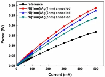
higher the reflectivity. This result is consistent with the SEM surface morphology results and the SIMS depth analysis dis-cussed above. The output power of the LEDs with the decou-pled contact mirrors is shown in figure 4 alongside with the LED with the conventional contact mirror. The output power of the LEDs with the decoupled contact mirror is significantly improved compared to that of the LED with the conventional contact mirror. For example, at forward current of 350 mA, the optical power has been increased from 128 mW for the refer-ence LED to 222 mW for the LED with the decoupled contact mirror, of which the contact layer is Ni (1 nm)/Ag (1 nm). This significant improvement is largely due to the much improved reflectance of the decoupled contact mirror.
As a contact mirror, in addition to the high reflectance, the forward voltage is of great importance as well. It is found that the forward voltage of the LEDs with the optimized decoupled contact mirror is comparable to and even better than that of the reference LED at high current beyond 350 mA, as shown
in figure 5. This indicates that the decoupled contact mirror also meets the requirement of high electrical performance of high power LEDs. It should be noted that the electrical prop-erty starts to degrade as the Ag thickness increases in the thin Ni/Ag contact as shown in figure 5. The forward voltage increases significantly which is mainly due to the increase of the turn-on voltage. It is critical to reveal the reason behind the elec-trical degradation and understand the mechanism of the contact formation in the decoupling of the contact and the mirror.
The four-probe contactless sheet resistance measure-ment is performed on the thin Ni/Ag contacts before and after annealing. The results are illustrated in table 1. From the table 1 it can be seen that before the annealing the thin Ni/Ag bilayer shows low sheet resistance from 4.65 kΩ/□ down to 87 Ω/□, which is typical for thin metal layers. However, after annealing the sheet resistance increases to around 100 kΩ/□ for all the three contact layers. The huge increase of the sheet resistance implies that the contact layers are no more metals but possibly metal oxides since the annealing is conducted in the O2 ambient. We also
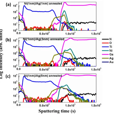
performed SIMS depth profile analysis to examine the com-position of the contact layers as shown in figure 6. It can be seen that compared the three contact layers, as the Ag thick-ness increases, Ni and Ag tend to inter-diffuse into each other. The Ni distribution is obviously broadening with the increase of Ag thickness. At the meanti me the O distribution coincides with those of Ni and Ag at the interface region. Based on the experimental results above, we propose the following contact Figure 3. Reflectivity measured for the samples of the conventional
contact mirror and the decoupled contact mirrors with thin annealed layer of Ni (1 nm)/Ag (1 nm), Ni (1 nm)/Ag (3 nm) and Ni (1 nm)/ Ag (5 nm), respectively.
Figure 4. Output power measured for LEDs with the conventional contact mirror and the decoupled contact mirrors with thin annealed layer of Ni (1 nm)/Ag (1 nm), Ni (1 nm)/Ag (3 nm) and Ni (1 nm)/ Ag (5 nm), respectively.
Table 1. Sheet square resistance of thin contact layers on top of p-GaN before and after annealing (Ω/□).
Type Non-annealed Annealed
Ni (1 nm)/Ag (1 nm) 4.65k 100.9k Ni (1 nm)/Ag (3 nm) 2.04k 97.98k
Ni (1 nm)/Ag (5 nm) 87 97.24k
Figure 5. Current–voltage (I–V ) curves measured for the LEDs with the conventional contact mirror and the decoupled contact mirrors with thin annealed layer of Ni (1 nm)/Ag (1 nm), Ni (1 nm)/ Ag (3 nm) and Ni (1 nm)/Ag (5 nm), respectively. The intercepts of the dashed lines on the X-axis indicate the turn-on voltages.
formation mechanism to explain the electrical characteristics of our decoupled contact mirrors. When the Ni/Ag contact layer is deposited and annealed in O2 ambient, since they are
very thin, they will be fully oxidized. As well known, thin Ni oxide forms ohmic contact (tunneling Schottky contact) with the p-GaN at the existence of Ag since Ag helps the out diffusion of Ga atoms from p-GaN which leaves large amount of Ga vacancies in the p-GaN and is beneficial to the ohmic contact formation. However, Ag oxide also forms a Schottky contact with the p-GaN which will add additional voltage drop for the devices to turn on. When the Ag oxide is as thin as 1 nm, due to the tunneling effect, the additional turn-on voltage is low. Therefore the forward voltage for the device with Ni (1 nm)/Ag (1 nm) contact layer is comparable to and even better than that of the device with the conven-tional contact mirror at high current beyond 350 mA. But as the Ag thickness increases in the Ni/Ag contact layer, thicker Ag oxide Schottky contact layer is formed and will add larger turn-on voltage as shown in figure 5. As an illustration for the case of thick Ni/Ag contact layer, if we assume the Schottky barrier height is solely determined by the difference of work functions and no tunneling effect is considered, since the work functions of Ag oxide and p-GaN are 5.6 eV and 7.5 eV, respectively, the Schottky barrier height will be 1.9 eV. This is in good agreement with the increase of the turn-on voltage for the device with Ni (1 nm)/Ag (5 nm) contact layer as shown in figure 6. When the silver is gradually decreased from 5 nm to 1 nm, the Schottky effect will be reduced due to the tunneling process. Therefore, as an optimized Ni/Ag
contact, a thin layer of Ag is desired which on one side can assist the Ga out diffusion and Ga vacancy formation, and on the other side can avoid the formation of the thick Ag oxide layer and reduce the turn-on voltage.
Besides the forward voltage, low reverse leakage current is also critically important for high-performance of LEDs. At 3 V reverse bias, the leakage currents for the reference, Ni (1 nm)/ Ag (1 nm), Ni (1 nm)/Ag (3 nm), Ni (1 nm)/Ag (5 nm) sam-ples are 4.8 × 10⁻⁸ A, 1 × 10⁻⁹ A, 5 × 10⁻⁹ A, 7 × 10⁻⁹ A,
respectively. The lowest reverse leakage current was observed in the proposed sample with Ni (1 nm)/Ag (1 nm), which has the superior electrical performance.
4. Conclusions
A novel decoupled contact mirror concept for the Ni/Ag/Ti/Au reflector of InGaN/GaN LEDs has been proposed and demon-strated. Both of high reflectivity and low forward voltage can be achieved at the same time through the proposed decoupled contact mirror which significantly improves the optical power performance of the LEDs. Through SEM and SIMS measure-ments, the effectiveness of the proposed contact mirror on suppressing the Ag agglomeration and the Ag intermixing has been proved. The mechanism of the decoupling of the contact and the mirror has also been investigated in detail. This new method provides an effective way for fabricating high perfor-mance contact mirrors and will contribute to the application of high efficient solid state lightings.
Figure 6. SIMS depth profiles of the decoupled contact mirrors with thin annealed layer of (a) Ni(1nm)/Ag(1nm), (b) Ni (1 nm)/Ag (3 nm) and (c) Ni (1 nm)/Ag (5 nm), respectively.
B Zhu et al
6
Acknowledgments
This work was supported by the National Research Founda-tion of Singapore under Grant No. NRF-CRP-6-2010-2. References
[1] Tan S T, Sun X, Demir H V and DenBaars S 2012 IEEE Photon. J.4 613
[2] Ju I, Kwon Y, Shin C-S, Kim K H, Bae S-J, Kim D-H, Choi J and Ko C G 2011 IEEE Photon. Technol. Lett. 23 1685 [3] Sang Kim K, Gyun Suh M and Cho S 2012 Appl. Phys. Lett.
100 061113
[4] Chang L-B, Shiue C-C and Jeng M-J 2007 Appl. Phys. Lett. 90 163515
[5] Chang L-B, Shiue C-C and Jeng M-J 2009 Appl. Surf. Sci. 255 6155
[6] Kim J-Y, Lee J-M and Kwon M-K 2012 Electrochem. Solid-State Lett.15 H198
[7] Jang H W and Lee J-L 2004 Appl. Phys. Lett. 85 4421 [8] González-Hernández R, López W, Ortega C,
Moreno-Armenta M G and Rodríguez J A 2010 Appl. Surf. Sci.256 6495
[9] Song J O, Ha J-S and Seong T-Y 2010 IEEE Trans. Electron Devices57 42
[10] Lee J-R et al 2005 J. Electrochem. Soc. 152 G92
[11] Sheu J, Su Y-K, Chi G-C, Koh P, Jou M, Chang C, Liu C and Hung W 1999 Appl. Phys. Lett. 74 2340
[12] Son J H, Song Y H, Yu H K and Lee J-L 2009 Appl. Phys. Lett.95 062108
[13] Ju Z et al 2013 Appl. Phys. Lett. 102 243504
[14] Wang Y, Cheng S, Wei Q, Ma E, Nieh T and Hamza A 2004 Scr. Mater.51 1023