Journal of Physics: Conference Series
Detectivity of YBCO transition edge bolometer:
modulation frequency, bias current and absorber
effects
To cite this article: A Moftakharzadeh et al 2008 J. Phys.: Conf. Ser. 97 012009
View the article online for updates and enhancements.
Related content
Dimension effect on the performance of carbon nanotubes nanobolometers Caleb Christianson, Rongtao Lu and Judy Wu
-A nanoscale YBCO mixer optically coupled with a bow tie antenna
Fredrik Rönnung, Sergey Cherednichenko, Dag Winkler et al.
-A simple high-temperature
superconducting thin-film optical bolometer B Dwir, L Pavesi, J H James et al.
-Recent citations
Investigation of CeO2Buffer Layer Effects on the Voltage Response of YBCO Transition-Edge Bolometers Roya Mohajeri et al -Roya Mohajeri et al -Mehdi Fardmanesh et al
-Detectivity of YBCO transition edge bolometer:
modulation frequency, bias current and absorber
effects
A Moftakharzadeh1, A Kokabi1, A Bozbey2,5,6, T Ghods-Elahi3, M Vesaghi3, S
Khorasani1, M Banzet4, J Schubert4, and M Fardmanesh1
1School of Electrical Engineering, Sharif University of Technology, Tehran, Iran 2Electrical Engineering Department, Bilkent University, Ankara, Turkey
3Department of Physics, Sharif University of Technology, Tehran, Iran 4ISG1-IT, Forschungszentrum Jülich GmbH, Juelich, Germany
Corresponding author: M Fardmanesh, Email: [email protected]
Abstract. Bolometric response and noise characteristics of YBCO superconductor transition
edge IR detectors with relatively sharp transition and its resulting detectivity are investigated both theoretically and experimentally. The magnitude of response of a fabricated device was obtained for different bias currents and modulation frequencies. Also dependency of intrinsic noise of the device on the bias current in the vicinity of critical temperature was studied for various values of chopping frequencies. Using the measured and calculated bolometric response and noise characteristics, we found and analyzed the device detectivity versus frequency for different bias currents. The detectivity versus chopping frequency of the device did not decrease following the response strongly, due to the decrease of the noise at higher frequencies up to 1KHz, resulting in maximum detectivity around the modulation frequency of 100Hz. We also improved the detectivity of the device through the increase of the surface absorption by using a novel infrared absorber, which is made of a Copper-Carbon composite, coated in a low temperature process. Within the modulation frequency range studied in this investigation, comparison of device responsivity before and after the coating is also presented.
1. introduction
Many works have been focused on the applications of the YBCO material in different types of the radiation detectors for the near to far infrared wavelength regime [1-6]. One of the popular types of these devices is transition-edge bolometers, the physical operation principle of which is based upon the steep drop in their resistance R, at the transition temperature, Tc [7]-[10].
This type of detector has relatively small noise level at its operating point and therefore potentially it can exhibit high detectivity values [11]. In this work we have investigated the effect of bias current and modulation frequency on the device detectivity. This has been done theoretically by noise and response analysis and experimentally by measuring these two parameters at different values of bias currents and chopping frequencies. While we could measure both the phase and magnitude of the response using our setup, in this paper we only focus on the magnitude of the response, which is used for the D* calculation and analysis. To the best of our knowledge this is for the first time that the D* of such devices versus chopping frequency is measured and analyzed for various bias currents.
5 His current address is : Department of Quantum Engineering, Nagoya University, Furo-cho, Chikusaku, Nagoya 464-8603, Japan
6 This work was partly supported by TUBITAK with project number 105E134
8th European Conference on Applied Superconductivity (EUCAS 2007) IOP Publishing Journal of Physics: Conference Series 97 (2008) 012009 doi:10.1088/1742-6596/97/1/012009
These devices typically do not reach their potentially high detectivity values due to the lack of absorption of YBCO as well as the substrate, especially in the micro-meter range. Our device absorption was not sufficiently high either, and only a little fraction of input power was absorbed by the device when using the bare YBCO film [11]. This resulted in a reduced detectivity and therefore it leads us to the use an absorption layer in order to compensate for this deficiency. Some difficulties arise when using usual absorbers due to their destructive effects on the electrical properties of the superconducting YBCO material. For example they can cause lowering the critical temperature Tc or
smoothening the transition curve. Smoothening and widening transition curve is an undesirable effect, which reduces peak value in dR/dT curves and hence reducing the IR response. YBCO thin film is very sensitive to higher temperatures and stresses, and hence coating methods which involve high temperature processing might be considerably destructive. In some low temperature methods, using solvents might also introduce harmful effects to the device. In this work, we introduce a novel absorber which was coated in a low temperature process and had very little destructive effect on our bolometer device. We also present the effect of this coating on the responsivity and the transition curve.
2. Theoretical Model
The voltage noise for this type of detectors is the device output signal, while we have blocked it from input radiation, leading to a value equivalent to the dark noise. The noise equivalent power (NEP), is defined as the input signal power that would give the dark noise level observed in the output. Various intrinsic noise sources in addition to Johnson noise near the transition temperature are expected in a superconducting thin film. This class of noises is primarily due to magnetic flux penetration and fluctuations in the order parameter in the film [12-16].
NEP together with the responsivity determine the detectivity (D*), which is obtained in terms of the measured values of infrared and noise response, as;
√
NEP 1 where A is the effective radiation absorption area of the detector, rv is the voltage responsivity, Vn is
the voltage noise, and Δf is the frequency band used in the voltage noise measurement [12].
The responsivity, defined as the output signal per watt of input signal, is important in respect to the detection of the smallest possible signals, limited by noise from the detector. The responsivity versus modulation frequency and temperature has been previously analyzed, which according to the simple RC model leads to [17-19]:
j2
d
d 2 in which, I is the dc bias current, η is the absorption coefficient, f is the modulation frequency, and Ct
and Gt are the total thermal conductance and capacitance of the bolometer, respectively. For high
frequency modelling, thermal diffusion length is defined as the characteristic penetration depth of the temperature variation into the substrate. Thermal diffusion length is determined from:
3 where cs and ks are specific heat per unit volume and thermal conductivity of the substrate material,
respectively [20]. Above a certain frequency, called knee frequency, thermal diffusion length becomes comparable to or smaller than the substrate thickness and therefore Ct and Gt are determined by
modulation frequency as [20]:
8th European Conference on Applied Superconductivity (EUCAS 2007) IOP Publishing Journal of Physics: Conference Series 97 (2008) 012009 doi:10.1088/1742-6596/97/1/012009
5 The above consideration of Gt and Ct in the analysis, results in a good approximation for the
considered frequency range in this work compared to that of the comprehensive 1D model introduced in [20]. As it is obvious from (2), responsivity for this type of devices decreases due to increase in the chopping frequency [18].
The total noise equivalent power for a HTSC bolometer is obtained from sum of separate noise components, which can be obtained from [21,22]
NEP 8 B 4 B 4 B ⁄ 6 where, kB is the Boltzmann’s constant, δ is the Stefan-Boltzmann constant, Tb is background
temperature, and A is the effective absorption area of the device. The terms of equation (6) describe the noise equivalent power caused by the radiation fluctuations of the background, phonon noise, thermal noise of the resistance of the bolometer, and low-frequency noise of 1/f type respectively. V1/f
is calculated from the empirical Hooge relationship, as follows;
/ H 7
where αH is the Hooge noise parameter, N is the current carrier density in the superconducting film,
and v is the volume of the film [21]. Term of granularity noise has not been included in equation (6) because as it is previously reported this noise has its major effect in very low bias currents [11,12].
By substituting numerical values in equation (6) we have obtained dependency of the above noise types versus the modulation frequency as shown in figure 1. Gt is replaced from equation (4) for above
the knee frequency, where it is not determined by the substrate-coldhead interface [23]. For Hooge parameter we deal with a wide range of values depending on the film. This value is chosen so that the 1/f noise knee frequency is around 10Hz, the result of which matched the best to that of our measured data. S is also derived from equation (2).
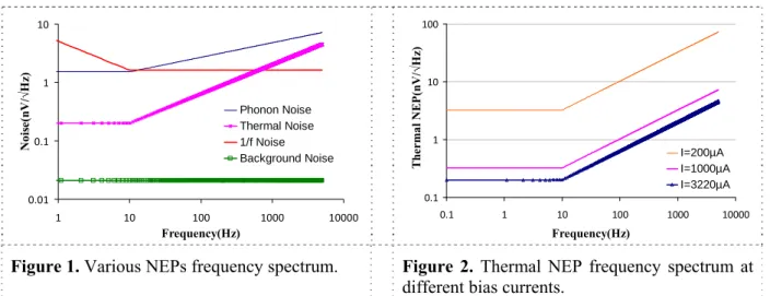
As it is understood from figure 1, the background NEP has trivial effect on ultimate noise equivalent power of the bolometer. Also at low frequencies thermal NEP could be neglected compared to the 1/f type and phonon NEP, where the 1/f noise is more dominated [22]. For middle frequencies NEP is approximately determined by phonon noise. Also as frequency increases, we observe more intense effect of thermal noise due to the decreased responsivity.
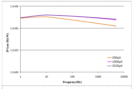
Figure 1. Various NEPs frequency spectrum. Figure 2. Thermal NEP frequency spectrum at different bias currents.
0.01 0.1 1 10 1 10 100 1000 10000 Frequency(Hz) No is e( nV /√ Hz ) Phonon Noise Thermal Noise 1/f Noise Background Noise 0.1 1 10 100 0.1 1 10 100 1000 10000 Frequency(Hz) T herm al NE P( n V /√ Hz ) I=200µA I=1000µA I=3220µA
8th European Conference on Applied Superconductivity (EUCAS 2007) IOP Publishing Journal of Physics: Conference Series 97 (2008) 012009 doi:10.1088/1742-6596/97/1/012009
From equation (6) it is concluded that only thermal NEP is related to bias current. For more analysis we have calculated the thermal NEP for three different currents as shown in figure 2. Following the results revealed in the figure, thermal NEP increases with decreasing the bias current and might have a major effect in very low bias currents in all over the frequency range.
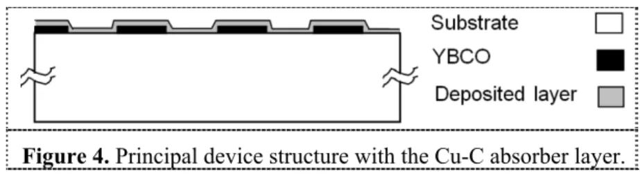
By using equation (1) we also have calculated the detectivity of the device versus chopping frequency at three different bias currents as shown in figure 3. As mentioned before, the only current dependent NEP is the thermal one and because of the minor effect of the thermal NEP at high bias currents, the detectivity is slightly affected by the higher values of bias current. This has been illustrated in the figure 3 for 1000µA and 3220µA bias currents. Also theoretical calculation proves that the dominance of 1/f NEP below the knee frequency, results in 20dB/decade slope of the detectivity curve for higher bias currents.
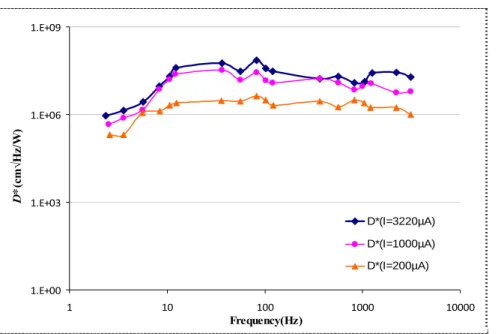
Figure 3. Detectivity versus frequency at three different bias currents. 3. Experimental Setup
The sample studied in this work was made of 200nm thin YBCO film on 1mm thick single crystal LaAlO3 substrate. The YBCO film was deposited by pulse laser deposition technique [24]. The device
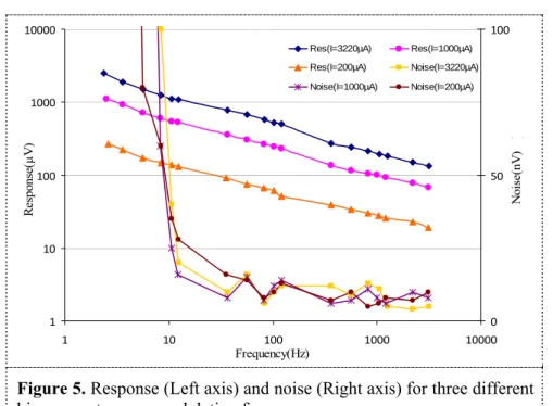
was patterned to spiral design with track width and spacing of 100µm. The samples were patterned using standard photolithography (positive photoresist) and the etching was carried on in about 0.75% dilute phosphoric acid. The active area of the patterns is 3.75mm2. For the contact pads of the YBCO pattern we deposited ~50nm thin gold layer after pre-etching YBCO using a dc planar magnetron etch-sputter unit. We used silver paste to make Cu wire contacts on the Au coated pads. The sample was characterized before and after the deposition of the absorption layer on it. The final structure of the device is shown in figure 4, which is further described and explained in the following sections.
1.E+00 1.E+03 1.E+06 1.E+09 1 10 100 1000 10000 Frequency(Hz) D* (c m √Hz/ W ) 200µA 1000µA 3220µA
8th European Conference on Applied Superconductivity (EUCAS 2007) IOP Publishing Journal of Physics: Conference Series 97 (2008) 012009 doi:10.1088/1742-6596/97/1/012009
Figure 4. Principal device structure with the Cu-C absorber layer.
The response of the sample was measured with a DC bias current Ibias, in four probe configuration
using an automated low-noise characterization setup. The temperature of the substrate was controlled with maximum 10mK deviation using a designed computer based PID controller. The developed characterization system is also capable of sweeping temperature with given various rate values. By setting this rate to 2Kmin-1 we have minimized the effect of the temperature gradient and its associated error, caused by the temperature rise between the temperature sensor and the sample. The phase and magnitude of the device was measured with a lock-in amplifier (SR830) using an ultra-low noise preamplifier (SR560) at its input. The employed radiation source was a mechanically modulated (with a mechanical chopper) blackbody with a temperature of 640K. We have chosen this temperature due to some limitation of our setup.
The resistance of the device was measured simultaneously with the phase and magnitude of the response in order to probe any deviation of magnitude of the response from the dR/dT curve.
4. Experimental results
4.1. Detectivity
The theoretical behavior of the detectivity versus frequency is already discussed in previous sections. The noise characteristics of this type of device versus temperature at different modulation frequencies are also reported previously [12]. Here we present the results of the measurements for the IR bolometric response and the noise versus modulation frequency at different bias currents of the device studied in this work, as shown in figure 5. The related comprehensive results and analysis are reported in [11]. Figure 5 shows that there is a low dependency of noise signal on the bias current. It also shows that noise signal below 10Hz is considerably high. Therefore the detectivity is perceptually low where we have acquired maximum response at this range of frequency. Above 10Hz, the obtained detectivity versus chopping frequency of the device did not decrease following the response. This is associated to the decrease of the noise at higher frequencies up to 1KHz, resulting in the maximum detectivity around 100Hz modulation frequency in our device.
8th European Conference on Applied Superconductivity (EUCAS 2007) IOP Publishing Journal of Physics: Conference Series 97 (2008) 012009 doi:10.1088/1742-6596/97/1/012009
Figure 5. Response (Left axis) and noise (Right axis) for three different
bias current versus modulation frequency.
As observed from figure 5, diminishing behaviors of response and noise versus frequency almost compensate each other, and we observe a nearly constant detectivity over the investigated frequency range.
Figures 3 and 6 show that the measured detectivity curves have many similarities to the theoretically predicted ones. i.e., in both of them increasing bias current at its low values improves detectivity, while it has very slight effect at higher values. Another similarity is that in both figures the detectivity has little variation in investigated frequency range. Below 10Hz detectivity falls under its average values of higher frequencies in spite of large response over the low frequency range. In the theoretical model, the slope of detectivity variation in this frequency range is 20dB/decade. But the measured slope is considerably higher and that the dependency of NEP to frequency does not follow the 1/f type, which is under further investigation.
Figure 6 shows lower value for detectivity at 200µA bias current with respect to the theoretical calculation presented in figure 3 especially at low frequencies. This might be associated to the granularity of the film that manifests itself at very low bias currents [11,12].
1 10 100 1000 10000 1 10 100 1000 10000 Frequency(Hz) R es pons e( µ V ) 0 50 100 No is e( nV) ) Res(I=3220µA) Res(I=1000µA) Res(I=200µA) Noise(I=3220µA) Noise(I=1000µA) Noise(I=200µA)
8th European Conference on Applied Superconductivity (EUCAS 2007) IOP Publishing Journal of Physics: Conference Series 97 (2008) 012009 doi:10.1088/1742-6596/97/1/012009
Figure 6. Detectivity versus frequency for three different bias currents.
4.2. Coating
Because of weak absorption of YBCO material in the IR range [12], surface coating is essential for increasing infrared response, particularly in the micrometer wavelength range. We deposited a novel absorber layer over the area of the patterned YBCO thin film. The absorber, used in this work, is a 100nm copper-carbon composite that is coated in a low temperature planar magnetron sputtering process. Copper-carbon film was prepared by a capacitance coupled RF-PECVD system with 13.56MHz power supply. The reactor consists of two electrodes with different area size. Smaller electrode was a copper metallic disk with 75mm diameter as powered electrode. The other electrode with 13cm diameter was grounded via the body of the stainless steel chamber. Deposition was performed on this electrode at room temperature. The chamber was evacuated to a base pressure of about 10-5torr prior to the deposition and then was raised to ambient pressure with controlled flow of
pure acetylene gas. Deposition of the film was performed in two steps. First a carbon layer was grown at 40W power and 0.05torr process pressure and 30 minutes deposition time resulting in about 100 nm thin layer. Then the copper-carbon layer was grown on it. For deposition of copper-carbon layer, RF power was 200W and process pressure was set at 0.025torr controlled by the gas flow. For a deposition time of 45 minutes a thickness of 100 nm was obtained for the Cu-C composite film resulting in a deposition rate of about 2.2 nm/min. Copper and carbon atomic content of the film were obtained from RBS analysis. As for the first try on the device, the atomic percentage of the Cu and C on the film was 55% and 45% respectively. By the control of the flow of acetylene and sputtering rate of Cu target, we were able to produce carbon films with different Cu composition.
Coatings may affect the device response in three different aspects. First, it can favorably increase absorption coefficient and therefore temperature variation caused by same incident infrared power resulting in higher response and higher D*. Second, it might smoothen the transition curve due to degradation of YBCO and so decreasing the dR/dT. This effect is not desirable as it decrease device response according to (2). Third, it might increase noise level of the device that is also another undesired effect. This may happen in two ways. At first, deposition of absorbing material may diminish the film quality and thus increase the noise level of the device. Secondly, by increasing
1.E+00 1.E+03 1.E+06 1.E+09 1 10 100 1000 10000 Frequency(Hz) D* (c m √ H z/ W ) D*(I=3220µA) D*(I=1000µA) D*(I=200µA)
8th European Conference on Applied Superconductivity (EUCAS 2007) IOP Publishing Journal of Physics: Conference Series 97 (2008) 012009 doi:10.1088/1742-6596/97/1/012009
absorption coefficient the background noise would also increase. But as background noise has a very little contribution in the total noise equivalent power of the device, this effect could be neglected.
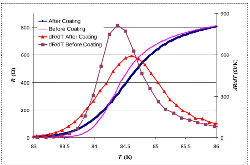
Figure 7. Transition (Left axis) and dR/dT (Right axis) versus
temperature at 100µA bias current.
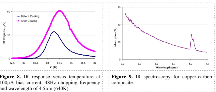
In figure 7 we observe that after coating, the transition has very slightly widened and therefore maximum value for dR/dT has dropped. This indicates that we have some degradation of the YBCO film after the coating. This figure shows that peak of dR/dT after coating is approximately %27 off from its original value before the coating. In figure 8 we present the measured value of IR response before and after the coating. Calculations reveal that the coating improves the response roughly by 78%. According to (2), since both measurements are done at the same bias current and chopping frequency, the following relation, which is based on dR/dT and surface absorption, can be used to derive the responsivity variations:
,after coating ,before coating after coating before coating d d after coating d d before coating 8 By comparing results of figure 7 and figure 8 and according to equation (8) it is found that the total surface absorption has increased by a factor of 2.4. Knowing the original device absorption to be about 7% and neglecting its reflection, the absorption of copper-carbon thin layer could be approximated to be about 10% at the radiation wavelength peak of 4.5µm. This approximation for value of absorption is the average of the overall absorption over the spectrum of the black body radiation. This approximately matches with our typical IR spectroscopy result for these composites that is also presented in figure 9. The observed peak in the absorption at 4.2µm in this figure might be partly associated to the special distribution and cluster size of the Cu species in the absorber layer, which is under further investigation.
The increase of the absorption by the composite layer is associated to both increase of the effective absorbing area and the total absorption of the layer in addition to the absorption of the YBCO film and
0 200 400 600 800 83 83.5 84 84.5 85 85.5 86 T (K) R ( Ω ) 0 300 600 900 dR /dT ( Ω /K ) After Coating Before Coating dR/dT After Coating dR/dT Before Coating
8th European Conference on Applied Superconductivity (EUCAS 2007) IOP Publishing Journal of Physics: Conference Series 97 (2008) 012009 doi:10.1088/1742-6596/97/1/012009
of the meander-line of the YBCO film. The detailed calculation and theoretical analysis of the above on the exact response behavior is under further investigation. Here we are considering the impact of the increase of the whole absorption caused by the absorber layer as a constant factor. This is found to be a good approximation for the considered frequency range, since the thermal diffusion length for this range is larger than the spacing within the lines of the meander-line pattern of the YBCO.
The change of copper doping in this type of composites strongly affects their absorption coefficient, which is under further investigation for finding the optimal doping level.
Figure 8. IR response versus temperature at
100µA bias current, 48Hz chopping frequency and wavelength of 4.5µm (640K).
Figure 9. IR spectroscopy for copper-carbon composite.
As also noticed from the variations in the transition curve in figure 8, there is a shift in maximum response with respect to the bias temperature. This phenomenon might be associated to the degradation of the YBCO due to diffusion of carbon into the material affecting mainly in the lower part of the transition curve, which caused the similar effect on the dR/dT curve shown in figure 7.
5. conclusion
In this work we have measured and calculated the bolometric response and the noise signal over the interest range of frequency and obtained its associated detectivity. Our investigation shows that the detectivity is nearly constant in the middle range of frequency and considerably drops at lower frequencies due to higher noise level in this range. This is associated to the considerable increase of the 1/f type noise in our device. Measured value for detectivity well matched the expected theoretical values in many aspects. We also used a new Cu-C composite absorber on the bolometers to increase the D* of the devices in the measured micrometer radiation range. The coating of the absorber had no major destructive effect on the electrical characteristic of the device and only degraded dR/dT slightly. The used thickness of the absorbing layer was as low as about 100 nanometers and no phase lag and thermal damp was observed for the investigated modulation frequency range. Because of the high percentage of copper in the deposited composite used in this work, the absorption coefficient improved by only about two times. A detectivity, D* in the range of 108cmHz0.5/W at about 100 Hz
modulation frequency was obtained for a blackbody radiation signal with peak value of about 4.5 micrometer. Effect of copper doping in the detectivity as well as in the degradation of the dR/dT of the devices is under further investigation.
References
[1] Rahman F 2006 Superconducting detectors in astronomy Contemp. Phys. 47 181 0 30 60 82.5 83 83.5 84 84.5 85 85.5 86 T (K) IR R esp on se ( µ V ) Before Coating After Coating 0 10 20 30 2.2 2.7 3.2 3.7 4.2 4.7 Wavelength (µm) A b so rp ti on (% )
8th European Conference on Applied Superconductivity (EUCAS 2007) IOP Publishing Journal of Physics: Conference Series 97 (2008) 012009 doi:10.1088/1742-6596/97/1/012009
[2] Delerue J, Gaugue A, Teste P, Caristan E, Klisnick G, Redon A and Kreisler A 2003 YBCO mid-infrared bolometer arrays IEEE Trans. Appl. Supercond. 13 176
[3] Brasunas J C and Lakew B 1994 High Tc superconductor bolometer with record performance Appl. Phys. Lett. 64 777
[4] Berkowitz S J, Hirahara A S, Char K and Grossman E N 1996 Low noise high-temperature superconducting bolometers for infrared imaging Appl. Phys. Lett. 69 2125
[5] Li Q, Fenner D B, Hamblen W D and Hamblen W G 1993 Epitaxial YBa2Cu3O7–y bolometers
on micromachined windows in silicon wafers Appl. Phys. Lett. 62 2428
[6] Bluzer N 1995 Analysis of quantum superconducting kinetic inductance photodetectors J. Appl.
Phys. 78 7340
[7] Kraus H Superconductive bolometers and calorimeters 1996 Supercond. Sci. Technol. 9 827 [8] Richards P L, Clarke J, Leoni R, Lerch Ph, Verghese S, Beasley M R, Geballe T H, Hammond
R H, Rosenthal P and Spielman S R 1988 Feasibility of the high Tc superconducting
bolometer Appl. Phys. Lett. 54 283
[9] Fardmanesh M, Scoles K and Rothwarf A 1998 DC characteristics of patterned YBa2Cu3O7-x
superconducting thin-film bolometers: artifacts related to Joule heating, ambient pressure, and microstructure IEEE Trans. Appl. Supercond. 8 69
[10] Hu Q and Richards P L 1989 Design analysis of a high Tc superconducting microbolometer Appl. Phys. Lett. 55 2444
[11] Kokabi A, Moftakharzadeh A and Fardmanesh M 2007 Investigation of the bias current and frequency dependence of the detectivity of high-Tc superconductor transition-edge IR
detectors ICEE 2007 Tehran
[12] Fardmanesh M, Rothwarf A and Scoles K J 1996 Noise characteristics and detectivity of YBa2Cu3O7 superconducting bolometers: Bias current, frequency, and temperature
dependence J. Appl. Phys. 79 2006
[13] Karmanenko S F, Semenov A A, Leonov V N, Bobyl A V, Dedoborets A I, Lunev A V, Nashchekin A V and Suris R A 2000 Sources of flicker noise and the technology of superconducting microstripes based on yttrium barium cuprate films Tech. Phys. 45 443 [14] Khrebtov I A 2002 Noise properties of high temperature superconducting bolometers Fluct.
Noise Lett. 2 (2002) R51
[15] Galeazzi M, Zuo F, Chen C and Ursino E 2004 Intrinsic noise sources in superconductors near the transition temperature Nucl. Inst. Meth. Phys. Res. A (2004) 520
[16] Nowak E R 2005 Flux-flow voltage noise and normal-state resistance fluctuations in epitaxial (Dy,Y)Ba2Cu3O7 thin films Physica C 421 15
[17] Nahum M, Verghese S, Richards P L and Char K 1991 Thermal boundary resistance for YBa2Cu3O7– films Appl. Phys. Lett. 59 2034
[18] Bozbey A, Fardmanesh M, Askerzade I N, Banzet M and Schubert J 2003 Effects of the superconductivity transition on the response of YBCO edge transition bolometers
Supercond. Sci. Technol. 16 1554
[19] Repsas K, Laurinavicius A, Vaskevicius A R and Anisimovas F 2001 Response of superconducting Y-Ba-Cu-O films to millimeter wave radiation Appl. Phys. Let. 79 4544 [20] Fardmanesh M 2001 Analytic thermal modeling for dc-to-midrange modulation frequency
response of thin-film high-Tc superconductive edge-transition bolometers Appl. Opt. 40 1080
[21] Khrebtov I A and Tkachenko A D 1999 High-temperature superconductor bolometers for the IR region J. Opt. Technol. 66 736
[22] Yi Song, Anupam Misra, Crooker P P and Gaines J R 1991 1/f Noise and Morphology of YBa2Cu307- 6 Single Crystals Phys. Rev. Lett. 66 825
8th European Conference on Applied Superconductivity (EUCAS 2007) IOP Publishing Journal of Physics: Conference Series 97 (2008) 012009 doi:10.1088/1742-6596/97/1/012009
of superconducting edge-transition YBa2Cu3O7-X bolometers through substrate properties Appl. Optics 38 4735
[24] Schubert J, Siegert M, Fardmanesh M, Zander W, Prömpers M, Buchal Ch, Judit Lisoni and Lei C H 2000 Superconducting and electro-optical thin films prepared by pulsed laser deposition technique Appl. Surf. Sci. 168 208
8th European Conference on Applied Superconductivity (EUCAS 2007) IOP Publishing Journal of Physics: Conference Series 97 (2008) 012009 doi:10.1088/1742-6596/97/1/012009