PERFORMANCE ANALYSIS OF THREE PORT FULL BRIDGE
CONVERTER FOR HYBRID PHOTOVOLTAIC/BATTERY
MANAGEMENT SYSTEM
byMehmet Akif SENOL*
Department of Electrical and Electronics Engineering, Faculty of Engineering and Architecture, Istanbul Gelisim University, Istanbul, Turkey
Original scientific paper https://doi.org/10.2298/TSCI180925332S
In this paper, performance analysis of three port full bridge converter based hybrid photovoltaic (PV)/battery management system is explained. The overall control system of the three port full bridge converter based PV/battery management system is created and simulated using MATLAB. Maximum power point tracking of solar PV system is controlled by perturb and observe method. Load regulation of PV/ battery management system is controlled by phase shift pulsewidth modulation technique. The system is tested for various real time operating conditions of the power system such as variation of PV panel voltage, change of battery voltage, and change of load power. The experimental verification also is carried out for developed system. Finally, simulation result and experimental result are compared for the developed system.
Key words: three port converter, hybrid power system, load regulation,
pulsewidth modulation, phase shifting pulsewidth modulation
Introduction
Hybrid power resources are the hopeful eco-friendly power sources for the future. Hy-brid power energy systems (HPES) offer constant and consistent energy supply to the custom-ers [1, 2]. Advanced power switched convertcustom-ers are the primary power modulating devices in HPES. But, the traditional HPES use separate power switched converter for each input energy sources. Therefore conventional HPES consist of several modulators, which derive themselves the demerits of, complicated system circuits, large number of switching elements, large power switching losses, bulky and costly. Multi energy source converters (MESC), also known as multi-port switching converter (MPSC), have been developed to the overcome this disadvan-tages of the traditional HPES. An MPSC consists of various renewable power energy sources in a single power modulating structure [3-8]. It offers the merits of compressed structure, simple circuit network, high stability, universal control and less fabrication cost and size [9-16].
In [3], a common approach to develop the multiport converters has been explained. First it presents the fundamental DC-DC converter structures such as boost, buck, boost/buck, cuk, zeta and SEPIC converters. In [4], systematic approach to develop multiport converters forms the use of basic pulsating sources cells. Using pulsating source cells, two categories of multiport converters are developed. In the first category of multiport converters, all the input Authorʼs e-mail: [email protected]
energy sources could deliver the load concurrently or independently. In the second category of multiport converters, only one energy source is permitted to transfer power to load at a time. In [5], introduces a very general topology of multiport converter with DC link and magnetic cou-pling. Then a three-port converter is taken as an example and different topologies of three-port converter are derived from the general topology. The author thus gives a method to derive dif-ferent topologies like DC link, magnetically coupled, combination of the both, current fed ports for a typical three-port converter. In [6], presents the static and dynamic analysis of multiport converters. The continuous averaged model of the multiport converter circuit is also presented. In [7], discussion on the selection of suitable topologies of multiport converters for any particular application. It gives set rules to identify the feasible topologies of multiport converters. In [8], presents the modeling of single diode PV arrays circuit model of a PV cell. It discusses design of PV with exhaustive equations governing the mathematical model of a PV array in simulink and explains all the terms regarding the design of the panel. With a practical panel being considered using the datasheet, it brings out the results on the characteristics of the PV panel model. It also includes the characteristics due to changes in the surrounding environmental conditions such as solar irradiation level and temperature level changes. In [9], presents a brief on the modeling of the single diode PV array model. It brings out the characteristics of the PV panel model due to changes in surrounding environmental conditions such as irradiation level and temperature level and also changes in the model parameters such as the diode parameters, variations in panel series and shunt resistances. It also presents an experimental set-up to validate the characteristics and an maximum power point tracking (MPPT) based on incremental conductance method. In [10], presents a typical three-port converter developed from full bridge converter structure. It uses only one full bridge converter to integrate three ports. The three port converter has been taken for a typical hybrid PV/battery system. It thus includes two unidirectional and one bidirectional storage port. Two autonomous control variables are identified to closely regulate flow of power between two ports and the third port provides power balance. A complete power management system which includes MPPT at the PV port and voltage regulation at the load port is also dis-cussed. In [11], describe the new DC link topology of three-port converter for hybrid PV/battery/ fuel cell (FC) application. It provides the complete switching state analysis of the converter during different operating modes of operation like with and without battery connected. It also gives a clear procedure to the dynamic modeling of the proposed converter. In [12], a new DC link topology of four port converter for hybrid renewable energy applications. It discusses the modeling of the individual components such as the fuel cell, PV panel, battery and the converter. It presents a structure for the power management system using pulsewidth modulation (PWM) technique. In [13], presents a new DC link topology of three-port converter employing zero voltage switching (ZVS). It gives a very useful explanation on the modes of operation of the con-verter during single and dual power supply situations, with the help of equivalent circuits in each mode and waveforms. In [14], presents a topology of three port converter employing bidirection-al hbidirection-alf bridge converters at bidirection-all the three ports and hence the name triple hbidirection-alf-bridge converter. It gives the modes operation of the converter and the control scheme using PWM plus phase shift control. It also provides the structure for the proposed control system and it presents the exper-imental validation also. In [15], presents an fully isolated topology of three port converter with two input ports are current fed. It uses multi winding transformer for fully provides the operating modes of the current fed converter and also the control principle based on PWM plus phase shift.
In this paper, load voltage regulation of three-port full bridge converter based hybrid PV/battery power system is analyzed. The three port converter integrates two input points and a load points. The topology of the three-port converter used in this application is developed from
full-bridge converter structure, hence referred to as three port full-bridge converter. This topol-ogy comes under partially isolated classifications of the converter topologies. The transformer provides isolation to the load port alone and the two input ports are at a common ground. Ob-jective of this paper is given as follows, simulink model of the three port full bridge converter which integrates a PV energy, a battery energy device and the load are developed using MAT-LAB/SIMULINK toolbox. In this work, centralized control structure for the converter which includes MPPT for the PV source and phase shifting algorithm for load voltage regulation. The power flow analysis of the converter in close loop with variations in panel voltage, variations in battery voltage and variations in load condition are explained. Real time hardware implemen-tation of three port full-bridge converter based hybrid PV/battery management system. Also comparison of simulation and hardware results for different operating modes are explained. Power flow analysis of the three port full bridge converter
based hybrid PV/battery management system
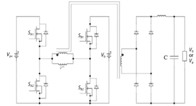
In this section power flow analysis of the closed loop control of three port full bridge converter based hybrid PV/battery management system is presented. A closed loop structure is developed for load voltage regulation and the power analysis for the system with load regulation is presented for different cases, such as variations in panel voltage, battery voltage, and varying load condition. The circuit diagram of three port full bridge converter is shown in fig. 1. Three port full bridge converter consists of a full-bridge converter, at the primary of the high frequency transformer, integrating PV source and battery. The full-bridge consists of two switching legs. The first leg with switches SA1 and SA2 connects the PV source and the second leg with switches
SB1 and SB2 connects the battery to the transformer. The secondary of the transformer feeds the
load after rectification using high frequency diode bridge rectifier and L-C filter.
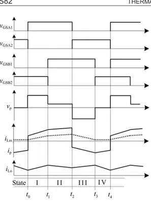
For the three port full bridge converter shown in fig. 1, we have four switching states (I-IV) available in a turn ON/OFF cycle. The ON/OFF position of the switches, equivalent circuit and equations for each switching
state are detailed as follows with respect to the fig. 2.
Before to, SA2 and SB2 are turned
ON and SA1 and SB1 are turned OFF,
while iLm freewheels throughout SA2
and SB2. At to, SA1 in ON and SA2 is OFF.
A positive voltage is appeared across the primary winding of the transformer’s. At
t1, SB2 is OFF and SB1 is ON. A positive
voltage is appeared across the primary winding of the transformer’s. At t2, SA1
is OFF and SA2 is ON. A negative voltage
is appeared across the primary winding of the transformer. At t3, SB1 is OFF and SB2 is ON. The
voltage appeared across the primary winding is clamped at zero, and iLm freewheels through SA2
and SB2. Four switching states/modes possible for the presented topology of full bridge tree-port
converter (TPC), which are summarized:
Mode I: Vp = Vpv SA1 and SB2 ON
Mode II: Vp = Vpv – Vb SA1 and SB1 ON
Mode III: Vp = –Vb SA2 and SB1 ON
Mode IV: Vp = 0 SA2 and SB2 ON
SA1 SA2 Vpv Vb V0 or Vp SB1 SB2
From the topology, it can be deduced that there are three control variables: the duty cycle of switch SA1, the duty cycle
of switch SB1, and the phase shift between
SA1 and SB1. Controlling SA1 controls the
PV port, controlling SB1 regulates battery
voltage/current and controlling the phase shift between them will control the load voltage.
But, for a TPC converter, the control degree of freedom is only two (in general, for an n-port converter, (n-1) degrees of control are possible). That is, only two ports could be controlled at a time and the third port could provide balance. Generally, the PV power port and the load power port are controlled continuously for MPPT at the PV power port and voltage regulation at the load port. At the same instance, the battery power port pro-vides power balance. In case of critical state of charge (SOC) of the battery, the control is transferred from PV power port to battery power port.
Hence, these four modes can be derived from a simple PWM scheme by introducing two degrees of control. Here, the two controls are the duty ratio and the phase shift. The duty ratio DA1 is controlled to control PV port and phase shift for load regulation. The second duty
ratio DB1 is dependent on DA1, because to retain the volt-sec stability of the magnetizing inductor
of the high frequency transformer. Thus at any time, the following two controls are possible;
Control 1 (Duty Ratio):
– The DA1 is controlled to control PV port and DB1 is derived from DA1 to maintain volt-sec
balance of transformer or,
– The DB1 is controlled to control battery port and DA1 is derived from DB1 to maintain
volt-sec balance of transformer.
Control 2 (Phase Shift):
Phase shift between DA1 and DB1 controls the output voltage.
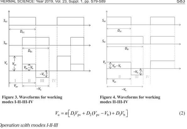
Operation with modes II-III-IV
By introducing the duty ratio and phase shift control, it is possible to have all the four modes or any three modes in a switching cycle. The modes II-III-IV with mode I absent is obtained by introducing no shift between SA1 and SB1 pulses, as depicted in fig. 3. The
corre-sponding expression for voltage at output is given in (1).
o 2( pv b) 3 b
V =n D V −V +D V (1)
Operation with modes I-II-III-IV
The modes I-II-III-IV can be obtained by introducing a small shift between SA1 and
SB1 pulses, as depicted in fig. 4. The corresponding expression for voltage at output is given in
eq. (2). vGSA1 vGSA2 vGSB1 vGSB2 iLm iLo State vp ip
Figure 2. Waveforms of FB-TPC showing switching states
o 1 pv 2( pv b) 3 b
V =n D V +D V −V +D V (2)
Operation with modes I-II-III
The modes I-II-III can be obtained by introducing a larger phase shift between SA1 and
SB1 pulses, as depicted in fig.5. The corresponding expression for voltage at output is given in
eq. (3).
o 1 pv 2( pv b) 3 b
V =n D V +D V −V +D V (3)
It can be inferred from the eqs. (1)-(3) that introducing phase shift between SA1 and
SB1 controls the output voltage. That is,
– With no phase shift, mode I is absent. It thus reduces the average output voltage.
– With small shift, mode I gets introduced in the output voltage waveform. Since mode I voltage (Vpv) is more positive than the mode II (Vpv-Vb), the introduction of mode I in-creases the average output voltage. Hence, by gradually increasing the phase shift, the average output voltage can be increased. – With very large phase shift, mode IV
van-ishes. Hence, the maximum possible aver-age voltaver-age for a given duty ratio occurs in this case.
The power flow analysis in close loop is done to maintain a constant load voltage (load voltage regulation) for three different cases namely, changes in panel voltage, battery voltage, and load conditions. The observations and tabulations for each case are presented.
DA1 DB1 SB1 Vpv Vpv Vpv – Vb Vp –Vb –Vb SA1
Figure 3. Waveforms for working modes I-II-III-IV DA1 DB1 SB1 SA1 Vpv Vpv – Vb Vp –Vb –Vb
Figure 4. Waveforms for working modes II-III-IV
Figure 5. Waveforms for operating modes I-II-III DA1 DB1 SB1 Vpv Vpv Vpv – Vb Vp –Vb –Vb SA1
Power flow analysis for changes in panel voltage
The tab. 1 shows the observations on power flow between the three ports for changes in panel voltage. The readings are tabulated for Vb = 6 V, DA1 = 0.4 to obtain rated output
volt-age of Vo = 4.2 V. Since the DA1 is made fixed, DB1 is dependent on panel voltage variations,
as because the ratio (Vpv/Vb) = (DB1/DA1) need to be maintained for volt-sec balance. Thus to
control the load voltage, the phase shift is controlled.
From the first set of readings, DA1 = 0.4, DB1 = 0.9333 and hence the range of
free-wheeling period (mode IV) is (1 – DB1) = 0.0666 which is 24°. This is the range of phase shift
available to control the output voltage.
But, as the panel voltage increases, DB1 increases and hence the range of shift
avail-able decreases. From tab. 1, as panel voltage increases from 8 V to 12 V, the range of phase shift decreases from 120° to 24°.
Table 1. Power flow analysis for panel voltage variations with DA1 = 0.4
Vpv
[V] [A]Ipv [W]Ppv [V]Vb [A]Ib [W]Pb I[A]mag [V]Vo [A]Io [W]Po DB1 of ϕ [°]Range [°]ϕ
12 3.18 38.16 6 –1.44 –4.38 2.33 4.01 4.10 16.436 0.933 24 0 11 2.79 30.69 6 –0.29 –8.63 1.35 3.93 4.02 15.815 0.866 48 20 10 2.79 27.9 6 –0.09 –2.84 1.68 3.97 4.05 16.092 0.800 72 45 9 2.91 26.19 6 0.62 18.68 1.41 3.98 4.07 16.236 0.733 96 69 8 2.76 22.08 6 1.20 36.03 1.14 3.93 4.01 15.772 0.666 120 93
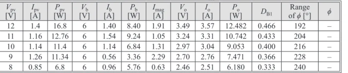
The actual phase shift needed to obtain the desired load voltage should be within the range of phase shift available. For panel voltage variations chosen from 8 V to 12 V, the actual phase shift required for load voltage regulation is well within the range of phase shift. The power flow analysis for changes in panel voltage is now repeated for Vb = 6 V and DA1 = 0.2. The observations are recorded in tab. 2. From the table, it is inferred that for the same range of panel voltage variations (from 8 V to 12 V), the actual phase shift, needed to maintain constant load voltage, is beyond the limit of maximum range of phase shift. It is because of very smaller duty ratio DA1. Hence for this case, the load voltage cannot be regulated.
Table 2. Power flow analysis for panel voltage variations with DA1 = 0.2
Vpv
[V] [A]Ipv [W]Ppv [V]Vb [A]Ib [W]Pb [A]Imag [V]Vo [A]Io [W]Po DB1 of ϕ [°]Range ϕ 12 1.4 16.8 6 1.40 8.40 1.91 3.49 3.57 12.482 0.466 192 – 11 1.16 12.76 6 1.54 9.24 1.05 3.24 3.31 10.742 0.433 204 – 10 1.14 11.4 6 1.14 6.84 1.31 2.97 3.04 9.053 0.400 216 – 9 1.26 11.34 6 0.56 3.36 2.29 2.70 2.76 7.471 0.366 228 – 8 0.85 6.8 6 0.96 5.76 0.63 2.46 2.51 6.180 0.333 240 –
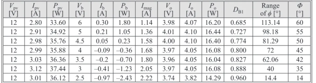
Power flow analysis for changes in battery voltage
A similar procedure is followed for power flow analysis for changes in battery volt-age. The readings are tabulated in tab. 3 for Vpv = 12 V, DA1 = 0.4 and Vo,ave = 4.2 V (desired).
The battery voltage is varied from 2 V to 6 V. For a fixed DA1 and Vpv, the duty ratio DB1 varies
with Vb as per volt-sec balance principle (Vpv/Vb)=(DB1/DA1). Hence as the battery voltage
de-creases, the range of phase shift available also decreases. Moreover, very small variations in battery voltage leads to greater reduction in the range of phase shift. Hence the battery voltage decides the strength of the system for load voltage regulation. Load voltage is almost regulated for battery voltage between 4.5-6 V. For Vb < 4.5 V, regulation is lost.
Table 3. Power flow analysis for battery voltage variations (DA1 = 0.4)
Vpv
[V] [A]Ipv [W]Ppv [V]Vb [A]Ib [W]Pb [A]Imag [V]Vo [A]Io [W]Po DB1 of ϕ [°]Range [°]Φ
12 2.80 33.60 6 0.30 1.80 1.14 3.98 4.07 16.20 0.685 113.14 60 12 2.91 34.92 5 0.21 1.05 1.36 4.01 4.10 16.44 0.727 98.18 55 12 2.98 35.76 4.5 0.05 0.23 1.58 4.00 4.10 16.40 0.774 81.29 50 12 2.99 35.88 4 –0.09 –0.36 1.68 3.97 4.05 16.08 0.800 72 45 12 3.03 36.36 3.5 –0.2 –0.70 1.80 3.96 4.05 16.04 0.827 62.06 42 12 3.12 37.44 3 –0.41 –1.23 2.05 3.97 4.05 16.08 0.888 40 35 12 3.01 36.12 2.5 –0.97 –2.43 2.22 3.74 3.82 14.29 0.960 14.4 14
Power flow analysis for changes in load condition
A similar analysis on power flow for changes in the load conditions are observed and tabulated as shown in tab. 4. The results are tabulated for Vpv = 70 V, Vb = 30 V, DA1 = 0.4 to
obtain desired load voltage of Vo = 42 V and for three different load conditions – half, 3/4th, and
full load.
Table 4. Power flow analysis for load variations (DA1 = 0.4)
Load Ipv
[A] [W]Ppv [V]Vb [A]Ib [W]Pb I[A]mag [V]Vo [A]Io [W]Po
Full 3.18 38.16 6 –1.44 –8.64 2.33 4.01 4.10 16.44
¾ 2.41 28.92 6 –1.10 –6.60 1.77 4.03 3.09 12.45
Half 1.65 19.80 6 –0.75 –4.50 1.20 4.05 2.07 8.38
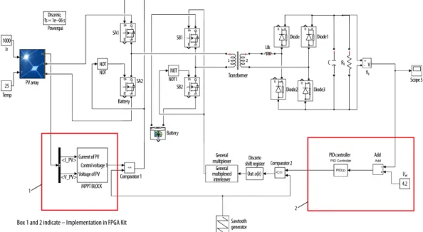
Experimental verification of three port full bridge converter based hybrid PV/Battery management system
The power circuit of the three port full bridge converter consists of a full-bridge con-verter with switches SA1, SA2, SB1 and SB2. The power MOSFET switches IRF840 are used to
build the power circuit. At the load end, a diode bridge rectifier is built using high frequency Schottky diodes 1N5819. Each power switch consists of the MOSFET switch IRF840 along with Opto-coupler and Driver circuit. As per gating requirement of the MOSFET, each switch should be driven by a gate pulse with different ground. Hence for each switch, different grounds derived by using four different DC supplies, op-coupler and driver circuit. Figure 6 shows the block diagram of the closed loop control of
three port full bridge converter based hybrid PV/battery management system. In this closed loop consist of two loop, one is used for load voltage regulation i. e., output voltage is sensed from the load side and it is compared with ref-erence voltage. Then error voltage is processed via voltage regulation controller and it produc-es control voltage for pulse generation unit and then its processed via shift register for produc-ing desired phase shift for load regulation. Sec-ond loop used for maximum power point track-ing of PV panel i. e., actual current and voltage of PV panel is sensed and processed via perturb and observe maximum power point tracking
Figure 6. Block diagram of closed loop control of three port full bridge converter based hybrid PV/battery management system
Puls generator Three-port converter PV array Battery Load 56 Ω/25 W Vo Vpv 6 V/4.5 AHr
controller. It provides pulse for three port converter to extract the maximum power from PV panel. The overall control algorithm i. e., voltage regulation and maximum power tracking al-gorithm has been created using FPGA. Pulse generation for the three port converter via analog circuit. The simulink model of closed loop control of full bridge three port converter based hybrid power system is shown in fig. 7.
1000 Ir Powergui Discrete, Ts = 1e–06 s PV array Temp NOT NOT 25 Battery NOT NOT1 SA1 SB1 SB2 SA2 Transformer Diode Diode1 Diode2 Diode3 C R0 V0 V LIk Scope 5 Battery Current of PV Comparator 1 Voltage of PV MPPT BLOCK Control voltage 1 <I_PV> <V_PV> Comparator 2 PID controller Discrete shift register General multiplexer General multiplexed
interleaver Out u(k)
Add <= Sawtooth generator 4.2 Vref 1 2 Box 1 and 2 indicate – Implementation in FPGA Kit
Figure 7. Simulink model of closed loop control of full bridge TPC based hybrid power system Hardware prototype for the TPC based hybrid power system is built with pulse generator developed both using analog circuits and in digital platform using FPGA. In this section, the detailed implementation of the pulse generation scheme using analog circuits/IC and its design are presented along with complete waveforms. The pulse generation scheme implemented using Analog circuits/IC and its block diagram is depicted in fig. 8. The block diagram consists of a linear ramp generator and two control voltage generators. The control voltages compared with ramp produces two switching pulses SA1 and SB1. Further, a phase
shift between them is obtained using flip-flops/shift registers. The control voltage and MPPT algorithm is compared with linear ramp generated and it produce the pulse for SA1 and
SA2. The control voltage from PID controller
is compared with linear ramp generated and it produces the pulse for shift register and mul-tiplexer and output of the mulmul-tiplexer is pulse for SB1 and SB2. The phase shifting between
pulses SA1 and SB1 can be produced by using
IC 74273 which is an Octal D-type flip-flop used as a shift register. Thus it can generate 8 different clock pulse shifts.
Figure 8. Block diagram of pulse generation scheme Shift register Mux Control voltage generator Control voltage generator Linear ramp generator VA1 + + – – VB1 SA1 SA2 SB1 SB2
Analysis of three port full bridge converter based hybrid PV/battery management system for various modes of operation
The hardware prototype of the full bridge TPC based hybrid power system is analyzed for various modes of operation. This is achieved by controlling the duty ratio and the phase shift. The various output waveforms and tabulation for different modes of operations are dis-cussed in the following sections.
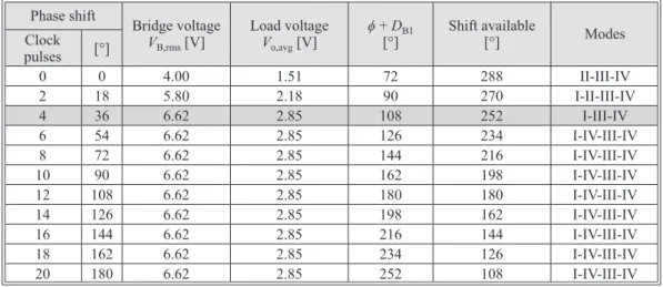
Analysis for DA1 = 0.1 and DB1 = 0.2
The duty cycle of switch SA1 is made fixed at 0.1 and hence the duty cycle of the
switch SB1 is determined based on it by the equation (Vpv/Vb) = (DB1/DA1). Since the
specifi-cations of the power circuit are chosen such that Vpv = 12 V and Vb = 6 V, the duty ratio DB1
is calculated to be 0.2. The tab. 5 gives the observations for different modes of operation with
DA1 = 0.1 and DB1 = 0.2. It is inferred from the tabulation, that the introduction of the mode I by
a small shift increases the average value of the load voltage. As phase shift increases, the dura-tion of Mode I also increases. A stage is reached where ϕ = DA1. Here, DA1 is 0.1 or 36°. Hence
when ϕ reaches 36o, the Mode II completely vanishes and there are only three modes present, namely, Modes I-III-IV. Now if the phase shift is further increased, there is no change in the modes of operation and hence the output voltage. This is because, a large duration of freewheel-ing mode IV is present and hence a great degree of freedom for phase is available. So, further increase in phase shift, just displaces the Mode III, but does not reduces/increases the Mode III.
When ϕ < DA1 and (ϕ + DB1) < 360°: Vo,avg increases as ϕ increases
ϕ > DA1 and (ϕ + DB1) < 360°: Vo,avg remains constant as ϕ increases
Table 5. Observations for different modes of operation with DA1 = 0.1 and DB1 = 0.2
Phase shift Bridge voltage
VB,rms [V] Load voltageVo,avg [V] ϕ + DB1[°] Shift available [°] Modes Clock pulses [°] 0 0 4.00 1.51 72 288 II-III-IV 2 18 5.80 2.18 90 270 I-II-III-IV 4 36 6.62 2.85 108 252 I-III-IV 6 54 6.62 2.85 126 234 I-IV-III-IV 8 72 6.62 2.85 144 216 I-IV-III-IV 10 90 6.62 2.85 162 198 I-IV-III-IV 12 108 6.62 2.85 180 180 I-IV-III-IV 14 126 6.62 2.85 198 162 I-IV-III-IV 16 144 6.62 2.85 216 144 I-IV-III-IV 18 162 6.62 2.85 234 126 I-IV-III-IV 20 180 6.62 2.85 252 108 I-IV-III-IV
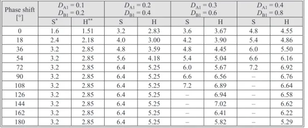
Comparison between simulation and hardware results
The voltage waveforms and the results presented in the previous sections for different duty ratios of DA1 and DB1 are compared with the simulation results here. A comparison table, between simulation and hardware results, is given in tab. 6. From the comparison, it is inferred and justified that the voltage waveforms from both hardware and simulation results are similar and the readings are matching closely.
Table 6. Comparison of load voltage values between simulation and hardware results
Phase shift [°]
DA1 = 0.1
DB1 = 0.2 DA1DB1 = 0.4 = 0.2 DA1DB1 = 0.6 = 0.3 DA1DB1 = 0.8 = 0.4
S* H** S H S H S H 0 1.6 1.51 3.2 2.83 3.6 3.67 4.8 4.55 18 2.4 2.18 4.0 3.00 4.2 3.90 5.4 4.86 36 3.2 2.85 4.8 3.59 4.8 4.45 6.0 5.50 54 3.2 2.85 5.6 4.18 5.4 5.04 6.6 6.16 72 3.2 2.85 6.4 5.25 6.0 5.67 7.2 6.92 90 3.2 2.85 6.4 5.25 6.6 6.56 – 6.76 108 3.2 2.85 6.4 5.25 7.2 6.89 – 6.64 126 3.2 2.85 6.4 5.25 – 6.94 – 6.58 144 3.2 2.85 6.4 5.25 – 7.02 – 6.62 162 3.2 2.85 6.4 5.25 – 6.41 – 6.22 180 3.2 2.85 6.4 5.25 – 5.82 – 5.29
* S – Simulated results, ** H – Hardware results Conclusion
Hybrid power energy systems (HPES) provide constant and consistent energy supply to the consumers. Power modulating converters are the most important power processing devic-es in HPES. In this paper is considered a three port full-bridge converter topology. Starting from explanation on the topology, principle and modes of operation, PWM generation to the power flow analysis, a detailed compilation of the theory and results has been presented in paper. De-tailed power flow analysis in closed loop in order to regulate load voltage, design and results on pulse generation scheme implemented using analog circuits and using FPGA and the hardware results validation are presented. The power flow analysis results are presented for three different conditions, such as variations in panel voltage, battery voltage and load condition. The imple-mentation of pulse generation scheme using analog circuits is dealt in detail. The maximum power point tracking and load regulation controller is implemented using FPGA kit and circuits for pulse generation, their design is presented. The results are presented for different sets of duty ratio and phase shifts. From the observations, it is justified that the control on phase shift controls the load voltage.
References
[1] Ioakimidis, C. S., et al., Solar Thermal and Wind Energy Applications, Thermal Science, 22 (2018), 5, pp. 2163-2176
[2] Fazelpour, F., et al.: Feasibility Study of Renewable Energy Resources and Optimization ... Thermal
Science, 21, (2017), 1A, pp. 335-351
[3] Liu, Y.-C., Chen, Y.-M., A Systematic Approach to Synthesizing Multi-Input DC-DC Converters, IEEE
Trans. Power Electron., 24 (2009), 1, pp. 116-127
[4] Li, Y., et al., Synthesis of Multi-Input DC-DC Converters, IEEE Trans. Power Electron., 25 (2010), 9, pp. 2372-2385
[5] Tao, H., et al., Family of Multiport Bidirectional DC-DC Converters, Proc. Inst. Elect. Eng., 153 (2006), 3, pp. 451-458
[6] Matsuo, H., et al., Characteristics of the Multi-Input DC-DC Converter, IEEE Trans. On Ind. Electron., 51 (2004), 3, pp. 625-631
[7] Kwasinski, A., Identification of Feasible Topologies for Multiple-Input DC-DC Converters, IEEE Trans.
Power Electron., 24 (2009), 3, pp. 856-861
[8] Villalva, M. G., et al., Modeling and Circuit-Based Simulation of Photovoltaic Arrays, Brazilian Journal
[9] Savita Nema, et al., Matlab/Simulink Based Study of Photovoltaic Cells/Modules/Array and their Exper-imental Verification, International Journal of Energy and Environment, 1 (2010), 3, pp. 487-500 [10] Wu, H., et al., Full-Bridge Three-Port Converters with Wide Input Voltage Range for Renewable Power
Systems, IEEE Trans. Power Electron., 27 (2012), 9, pp. 3965-3974
[11] Nejabatkhah, F., et al., Modeling and Control of a New Three-Input DC-DC Boost Converter For Hybrid PV/FC/Battery Power System, IEEE Trans. Power Electron., 27 (2012), 5, pp. 2309-2324
[12] Hosseini, S. H., et al., Multi-Input DC Boost Converter for Grid Connected Hybrid PV/FC/Battery Power System, IEEE Electrical Power & Energy Conference, Halifax, Canada, 2010
[13] Wai, R. J., et al., Newly Designed ZVS Multi-Input Converter, IEEE Trans. Ind. Electron., 58 (2011), 2, pp. 555-566
[14] Tao, H., et al., Three-Port Triple-Half-Bridge Bidirectional Converter with Zero-Voltage Switching, IEEE
Trans. Power Electron., 23 (2008), 2, pp. 782-792
[15] Chen, Y.-M., et al., Multi-Input DC/DC Converter Based on the Multiwinding Transformer for Renew-able Energy Applications, IEEE Trans. Ind. Electron., 38 (2002), 4, pp. 1096-1104
Paper submitted: September 25, 2018 Paper revised: November 5, 2018 Paper accepted: November 22, 2018
© 2019 Society of Thermal Engineers of Serbia Published by the Vinča Institute of Nuclear Sciences, Belgrade, Serbia. This is an open access article distributed under the CC BY-NC-ND 4.0 terms and conditions