An Analysis for the Broad-Band Absorption Enhancement Using
Plasmonic Structures on Uncooled Infrared Detector Pixels
Sevil Z. Lulec
1, Seniz E. Kucuk
1, Enes Battal
2, Ali K. Okyay
2, M. Yusuf Tanrikulu
1,
and Tayfun Akin
1, 31
METU-MEMS Research and Applications Center, Middle East Technical Univ., Ankara, Turkey
2
Dept. of Electrical and Electronics Engineering, Bilkent University, Ankara, Turkey
3
Dept. of Electrical and Electronics Engineering, Middle East Technical University, Ankara, Turkey
ABSTRACT
This paper introduces an analysis on the absorption enhancement in uncooled infrared pixels using resonant plasmon modes in metal structures, and it reports, for the first time in literature, broad-band absorption enhancement using integrated plasmonic structures in microbolometers for unpolarized long-wave IR detection. Different plasmonic structures are designed and simulated on a stack of layers, namely gold, polyimide, and silicon nitride in order to enhance absorption at the long-wave infrared. The simulated structures are fabricated, and the reflectance measurements are conducted using an FTIR Ellipsometer in the 8-12 m wavelength range. Finite difference time domain (FDTD) simulations are compared to experimental measurement results. Computational and experimental results show similar spectral reflection trends, verifying broad-band absorption enhancement in the spectral range of interest. Moreover, this paper computationally investigates pixel-wise absorption enhancement by plasmonic structures integrated with microbolometer pixels using the FDTD method. Special attention is given during the design to be able to implement the integrated plasmonic structures with the microbolometers without a need to modify the pre-determined microbolometer process flow. The optimized structure with plasmonic layer absorbs 84 % of the unpolarized radiation in the 8-12 m spectral range on the average, which is a 22 % increase compared to a reference structure with no plasmonic design. Further improvement may be possible by designing multiply coupled resonant structures.
Keywords: Infra-red imaging, microbolometer, surface plasmon polaritons, absorption enhancement.
1. INTRODUCTION
Plasmons are collective electron oscillation waves that can be excited at a metal-dielectric interface (surface plasmons) or confined around metal nanoparticles (localized plasmons). The principles of this excitation and dispersion of plasmons is well understood for a while now, and the plasmonics is increasingly finding applications in diverse fields with the advent of fabrication technology and availability of powerful computational resources [1]. The strong localization of the plasmonic mode allows for subwavelength waveguiding, non-linear applications, extraordinary transmission through subwavelength optical apertures, and ultra-compact photonic devices [2-4]. Furthermore, the strong plasmonic mode localization is advantageous for surface related phenomena such as highly sensitive chemical or biological detection using surface plasmon resonance sensors and surface enhanced Raman spectroscopy (SERS) applications [4-6]. In addition to these, there is an enormous research effort on utilization of localized and surface plasmons for absorption enhancement in thin film solar cells, where photovoltaic conversion efficiency is limited due to low optical absorption of the solar spectrum ( = 300-1100 nm) in the thin film active layer [7-9]. Recently, there is an increasing interest on the integration of plasmonic structures for enhanced infrared (IR) applications such as optical detection in the near and short-wavelength infrared [10-11] and surface enhanced infrared spectroscopy (SEIRS) [14]. There are, however, limited reports on mid- and long-wave IR applications [12-13], and they are mostly focused on wavelength selective applications.
This paper investigates the effect of plasmonic structures for broad-band absorption enhancement in the long-wave IR (LWIR) 8-12 µm wavelength region for imaging applications. The obtained absorption enhancement directly affects the sensitivity of the microbolometer pixels. Thus, the use of plasmonic structures can lead to sensitivity-enhanced microbolometers without the need of changing the pre-determined fabrication process significantly, and consequently, with almost no additional cost.
Section 2 provides a brief theoretical discussion on the origins of the increased absorption due plasmonics, and Section 3 reports the comparison of simulation and measurement results of a simple metal-dielectric stack, with integrated plasmonic layer on top of it, for the proof of concept. Then, Section 4 presents a microbolometer pixel structure and the sub-region of the pixel, which is modified by the plasmonic structures; this section also includes the obtained broad-band absorption enhancement characteristics in the 8-12 µm wavelength range by introducing plasmonic structures to the sub-region of interest. Finally, Section 5 summarizes the achievements obtained through the paper and comments on the results obtained using plasmonic layer on the microbolometer pixel structure.
2. BACKGROUND
Microbolometers are the most popular type uncooled thermal detectors, and today’s microbolometers mostly use a thermally sensitive resistor which is implemented on a thermally isolated bridge like structure that absorbs an induced infrared power, increasing its temperature and resulting in a change in the resistance. The absorption performance linearly determines the responsivity of a microbolometer. The increased absorption for a fixed IR power decreases noise equivalent temperature difference (NETD), which is one of the most important specifications of the IR imagers representing the sensitivity of focal plane arrays (FPAs). Microbolometers are usually preferred to have minimal top metal coverage, as metals are known to reflect nearly all of the incident energy at IR frequencies due to their perfect electric conductor (PEC) characteristics. However, increasing metal coverage with carefully designed structures may increase the of IR radiation absorption in microbolometers, as the IR photon energy can be coupled into a collective electron oscillation mode, namely surface plasmon mode, which is sustained between the metal surface and the dielectric. The coupling efficiency of the surface plasmon mode could be increased using grating structures or resonant effects. Grating structures and resonant effects may trigger surface plasmon polaritons, i.e., propagating waves at the metal-dielectric interface, which effectively increase the optical path length within the absorbing layer. Another advantage of surface plasmon modes for microbolometer applications is that the oscillating electrons in the metal due to resonant effects result in ohmic losses and strong attenuation, transferring their energy into heat and contributing to the total absorbed IR energy in the microbolometer structure.
3. ANALYSIS OF THE METAL-DIELECTRIC STACK
Figure 1 shows a 3D drawing of the basic metal-dielectric stack section, which is initially used to investigate the effect of the plasmonic structures on the absorption of the silicon nitride layer. The designed metal-dielectric structure is basically a stack of polyimide, silicon nitride, and gold layers. A bottom gold layer is introduced to confine the incoming light inside the 2-µm-thick polyimide layer, and by this way to increase the absorption of the whole structure. The polyimide layer is followed by the silicon nitride layer, and the silicon nitride layer is pursued by co-centric metallic square rings, as the plasmonic layer. Both the plasmonic and the bottom gold layers are implemented using 100-nm-thick gold and 20-nm-thick chromium as an adhesion promoter layer. A reference structure with no top metallic layer and two metal-dielectric stacks with different size co-centric metallic square rings are produced. The co-centric metallic square rings to be fabricated on top of the metal-dielectric stacks are chosen from the ones having distinct spectral absorption characteristics from the reference structure.
3.1 Micro Fabrication
The first step of the metal-dielectric process flow is sputtering bottom 20 nm chromium and 100 nm gold layers, which acts as a reflective mirror, on a 4” silicon wafer. A polyimide layer with a thickness of 2 µm is spin-coated on top of this mirror layer, which is used as a sacrificial layer in the microbolometer processes. Then, the silicon nitride layer is deposited as a structural layer, completing the reference structure. An additional chromium/gold bilayer is deposited and patterned for the formation of the plasmonic structures. The minimum feature size is chosen as 1 µm due to equipment limitations, and the simulations are conducted considering this dimension specification. Plasmonic structures are patterned using dry etching in a metal RIE system in order to fabricate structures with small critical dimensions as accurately as possible. Figure 2 shows scanning electron microscope (SEM) images of the produced co-centric metallic square rings structures with the dimension parameters, while Table 1 lists the target and measured dimensions of the structure with L2, L1, W, and P, representing the outer ring side length, inner ring side length, width, and period of the metallic rings, respectively. The widths of the inner and outer rings are equal to each other, and the period of the structures are the same both in x and y dimensions. Furthermore, the plasmonic rings are designed and simulated as perfect squares. However, the corners of the fabricated rings are rounded during the exposure in the aligner. The rounded-corner problem can be solved by exposing the photoresist in a precise exposure system such as a stepper.
r
I..
LI
A L
L2 L1 W P a Designed Produced Designed Produced Designed Produced Designed Produced Structure 1 8.0 µm 8.2 µm 4.0 µm 4.2 µm 1.0 µm 1.2 µm 10.0 µm 10.0 µm Structure 2 9.0 µm 9.2 µm 5.0 µm 5.2 µm 1.0 µm 1.2 µm 10.5 µm 10.6 µm
Figure 1. A 3D drawing of the basic metal-dielectric stack section, which is initially used to investigate the effect of the plasmonic structures on the absorption of silicon nitride layer. Light source propagation, E-field, and H-field directions for s and p polarizations, which are used during the FDTD simulations and also in the measurements, are also indicated.
Figure 2 . The SEM images of the produced co -centric metallic square rings plasmonic structures on the basic metal-dielectric stack , ( a) Structure 1, ( b) Structure 2. The dimension parameters of the co-centric square rings are also
indicated in (a).
Table 1. The designed and produced dimensions of the co-centric metallic square rings plasmonic structures.
20 nm / 10 0 nm 200 nm 2 µm 20 nm / 10 0 nm Chromium / Gold Silicon Nitride Polyimide 30 ° S pol. 30 ° P pol. x z b) a) 5 μm 5 μm L 2 L 1 W P
3.2 Simulation and Measurement Comparison
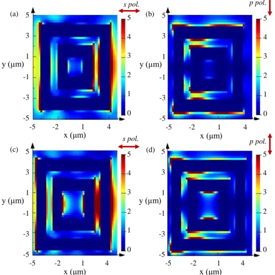
The reference and metal-dielectric stack structures are simulated using FDTD Solutions, Lumerical Inc, by using the necessary refractive index data from various sources for the 8-12 µm wavelength range. The silicon nitride refractive index data are measured using the FTIR Ellipsometer; whereas, comparably more complex polyimide refractive index data is taken from the literature [15]. Optical constants for gold and chromium layers are obtained from the database of the software, which uses data from [16-18]. To verify the simulations, reflection measurements are performed on fabricated structures using the FTIR Ellipsometer, which has a minimum 30˚ incidence light. Figure 1 also shows the light source propagation, E-field, and H-field directions for s and p polarizations, which are used to perform simulations and measurements. Figure 3 shows the simulated square of the electric field magnitude maps on the metal dielectric interfaces of the two different plasmonic structures for s and p polarizations, from which the coupling effects between the inner and outer rings and the high electric field intensity around the plasmonic structures can be seen clearly. The asymmetric electric field characteristic is due to the 30˚ incidence angle.
A 4
b
Figure 3. The simulated square of the E-field magnitude on the metal dielectric interface of the metal-dielectric stack. Arrows on the top right side of the graphics indicate the polarization directions of the E-field. (a-b) Structure1 for s and p polarized light, respectively, (c-d) Structure 2 for s and p polarized light, respectively. The light propagates having a 30° incidence angle with respect to the yz plane at 10.7 µm wavelength, at which the maximum absorption occurs.
Experimental absorption values are measured by obtaining reflection, R(), from the produced structures with the FTIR Ellipsometer. Figure 4 shows the spectral absorption measured and simulated by 1-R() in the 8-12 µm wavelength range with s polarized light for the reference structure, Structure 1, and Structure 2. The FDTD simulation results and experimental absorption strongly agree, showing similar spectral trends. For Structure 1 and Structure 2, the measured
(a) (b) (c) (d) s pol. s pol. p pol. p pol. 5 3 1 -1 -3 -5 -5 -2 1 4 5 4 3 2 1 0 x (μm) y (μm) 5 3 1 -1 -3 -5 -5 -2 1 4 5 4 3 2 1 0 x (μm) y (μm) 5 3 1 -1 -3 -5 -5 -2 1 4 5 4 3 2 1 0 x (μm) y (μm) 5 3 1 -1 -3 -5 -5 -2 1 4 5 4 3 2 1 0 x (μm) y (μm)
100 90 80 -' 70 60 50 40 C) 30 20 10 0 Simulation Data Measurement Data 80 8,5 90 9,5 10,0 10,5 11,0 11,5 12,0 Wavelength (tim) 100 90 80 '-' 70 60 50 0 40 0
:
30 0 80 85 9,0 9,5 10,0 10,5 Wavelength (jm) 1,0 11,5 12,0 10 20-k
Simulation Data -Measurement Data 100 90- 80--' 70-50 0 C) 40 C) 30- 20-10 0 80 Simulation Data Measurement Data 85 90 9,5 10,0 10,5 11,0 11,5 12,0 Wavelength (tim)absorption is greater than the simulated values. This is attributed to enhanced coupling of IR radiation to plasmonic modes due to metal surface roughness related to deposition step and metal sidewall roughness, potentially due to the dry etching step.
Figure 4 . The simulation and measurement spectral 1-reflection characteristics of ( a) reference structure, ( b) Structure 1, and ( c) Structure 2 with 30˚ incide nce angle light illumination for s-polarized light in the 8- 12 μm wavelength ran ge .
4. MICROBOLOMETER PIXEL ABSORPTION ENHANCEMENT SIMULATIONS
USING PLASMONICS STRUCTURES IN THE 8-12
µ m WAVELENGTH RANGE
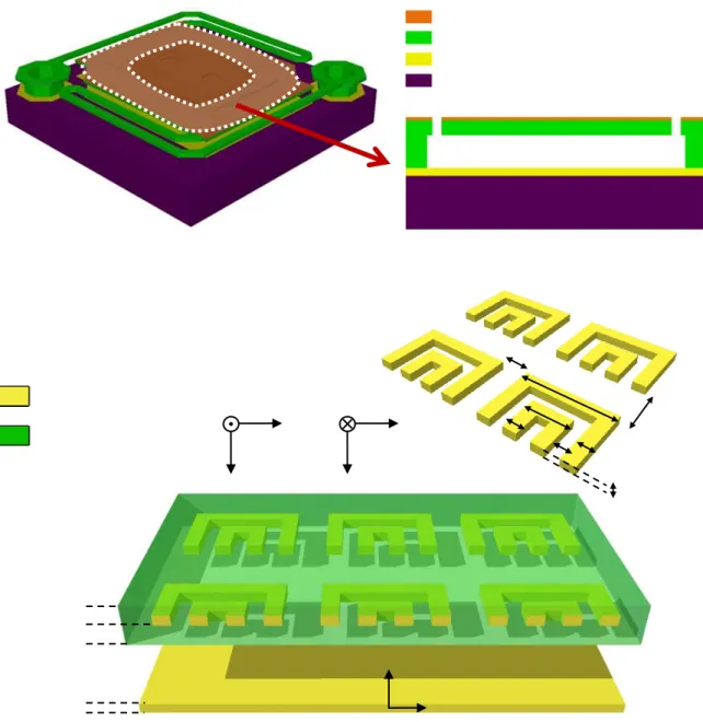
The responsivity of a microbolometer pixel is directly proportional to the absorption coefficient of the pixel, which can be derived, first by calculating the absorption coefficients of the sub-regions of the pixel using a cascaded transmission line model, and then taking the weighted average of the calculated absorption coefficients [19]. Thus, an increase in the absorption coefficient of a sub-region will lead to an increase in the total absorption coefficient of the pixel by the area of the sub-region. Figure 5 (a) shows the CAD drawing of the microbolometer pixel, the absorption value of which is desired to be enhanced by adding plasmonic structures, while Figure 5 (b) shows the cross sectional view of the largest area sub-region used in the simulations as the reference (no plasmonic design) case.
The plasmonic structures are designed in the same layer with the bottom electrodes of the pix el in order avoid any modification to the pre-determined microbolometer process flow. Thus, only a single mask design will be modified for
adding the plasmonic structures to the microbolometer pixel. Figure 6 shows a 3D drawing of the simulated microbolometer pixel sub-region including the plasmonic structures, while excluding the thin absorber layer shown in
Fig. 5 (b), which is also neglected in the FDTD simulations. The simulated sub-region involves the 400- nm -thick silicon nitride structural layer with buried plasmonic structures (50-nm-thick gold and 10-nm-thick chromium), 2-µm -thick air gap, and a bottom 100-nm-thick gold layer as the back-side reflector, followed by a 20 nm chromium adhesion layer.
(a) (b)
Absorber Structural Layer Mirror
- Substrate
Figure 6 also shows the simulated double C-shaped plasmonic structure that yielded the maximum broad-band
absorption enhancement in the 8-12 µm wavelength range with the dimension parameters . The dimensions of the double
C-shaped plasmonic structure can be listed as L2, L1, W, and D are equal to 3.5 µm, 1.5 µm, 0.5 µm , and 4 µ m, respectively.
Figure 5. (a) The CAD drawing of the microbolometer pixel. (b) The cross sectional view of the sub-region used in the FDTD simulations as the reference (no plasmonic design) structure.
Figure 6. A 3D drawing of the microbolometer pixel simulated sub-region with plasmonic layer included (silicon nitride layer is drawn transparent in order to show the plasmonics structures). The inset shows the dimension parameters of the
double C-shaped plasmonic structures. Light source propagation, E-field, and H-field directions for s and p polarizations , which are used during the FDTD simulations, are also indicated.
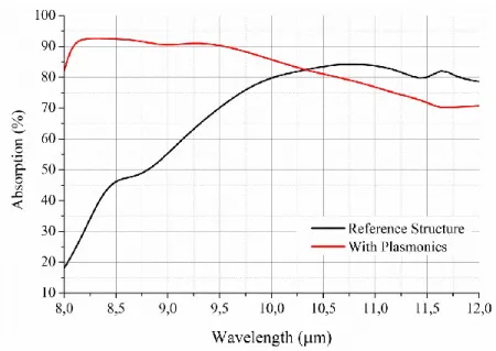
Figure 7 shows the simulated square of the electric field magnitude maps around the metal dielectric interface for s and p polarized light propagating in the z-direction. Besides, Figure 8 shows the spectral absorption characteristics comparison of the reference, i.e. without plasmonic structure, and double C-shaped plasmonic structure for the unpolarized light. As can be seen from the Figure 8, the double C-shaped metallic structures increase the absorption in
the 8-10 µm wavelength range considerably. The 8 -12 µm wavelength range unpolarized light average absorption value is increased from 69 %, without plasmonic structures, to 84 %, corresponding to 22 % absorption enhancement.
L 2 D D W W W L 1 T 200 nm 200 nm 2 µm 20 nm / 100 nm Chromium / Gold Silicon Nitride x z S pol. P pol. Absorber Layer Structural Layer Mirror Substrate (a) ( b )
100 -90 80 7 60-0 50 C -C 30 20 10 Reference Structure - With Plasmonics 80 85 90 9,5 10,0 10,5 11,0 Wavelength (tm) 11,5 12,0 aaaaa
Figure 7 . The simulated square of the E-field magnitude in the xy cross-section on the metal/dielectric interface for
( a) s polarized light and (b) p polarized light, with the incidence light propagates through – z direction at 9,5 μ m wavelength. Arrows on the top right side of the graphics indicate the polarization directions of the E-field.
Figure 8 . The simulated spectral absorption characteristics of the reference (without plasmonic) structure and the structure
involving double C-shaped metallic gold layer (with plasmonics) in the 8- 12 μm wavelength ran ge for unpolarized light shown with black and red lines, respectively.
5. CONCLUSION
This study reports broad-band absorption enhancement in the LWIR using plasmonic structures. A metal-dielectric stack employing co -centric metallic square rings is designed, simulated, and fabricated. FDTD methods are employed for the
simulations, which are verified by FTIR Ellipsometer reflection measurements. The trends of the designs with and without plasmonic structures match for both the simulation and the measurement results. The slight difference between the simulation and measurement results can be attributed to the microfabrication imperfections. Furthermore, a microbolometer pixel is investigated to obtain broad-band absorption enhancement using plasmonic structures computationally. The largest area sub-region, which dominates the absorption of the microbolometer pixel, is
selected for the FDTD simulations. Th is sub-region is simulated by including the double C-shaped plasmonic structure ,
(a) s pol. (b) p pol.
x (μm) y (μm) 3 1 - 1 - 3 - 3 - 1 1 3 14 12 10 8 6 4 2 0 x (μm) y (μm) 3 1 - 1 - 3 - 3 - 1 1 3 14 12 10 8 6 4 2 0
and 22 % absorption enhancement is computationally achieved, which leads to 84 % average absorption in the 8-12 µm wavelength range for the unpolarized light. The absorption is directly related with the NETD of the microbolometer pixels. Therefore, the reported enhancement in the absorption will lead to a decrease in NETD values. Moreover, the reported absorption enhancement is achieved without changing the pre-determined process steps of the microbolometer fabrication. Therefore, implementation of plasmonics for LWIR broad-band applications opens up new horizons for increased responsivity IR imaging with almost no additional cost. The enhancement in the absorption coefficient of the microbolometer pixel can also be investigated by optimizing the placement of plasmonic structures within the structural layer at the expense of modifying the process flow, paving the way for further improvements.
ACKNOWLEDGEMENTS
The authors would like to thank Basak Kebapci, Taha A. Yogurt, Eren Canga, and Akin Aydemir for their contributions and support in the simulations and fabrication.
REFERENCES
[1] Maier, S. A., [Plasmonics: Fundamentals and Applications], Springer, New York (2007).
[2] Tang, L., Kocabas, S. E., Latif, S., Okyay, A. K., Ly-Gagnon, D.-S., Saraswat, K. C. and Miller, D. A. B., “Nanometre-scale germanium photodetector enhanced by a near-infrared dipole antenna,” Nature Photonics 2, 226-229 (2008).
[3] Schuller, J. A., Barnard, E. S., Cai, W., Jun, Y. C., White, J. S. and Brongersma, M. L., “Plasmonics for extreme ligth concentration and manipulation,” Nature Materials, Vol. 9, 193-204 (2010).
[4] Flory, F., Escoubas, L., and Berginc, G., “Optical properties of nanostructured materials: a review,” Journal of Nanophotonics, Vol. 5, 052502 (2011).
[5] Yao, X., Li, X., Toledo, F., Zurita-Lopez, C., Gutova, M., Momand, J. and Zhou, F., “Sub-attomole oligonucleotide and p53 cDNA determinations via a high-resolution surface plasmon resonance combined with oligonucleotide-capped gold nanoparticle signal amplification,” Anal. Biochem., Vol. 354, No. 2, 220-228 (2006).
[6] Bell, S. E. J. and Sirimuthu, N. M. S., “Surface-enhanced raman spectroscopy (SERS) for sub-micromolar detection of DNA/RNA mononucleotides,” Journal of American Chemical Society, Vol. 128, No. 49, 15580-15581 (2006).
[7] Atwater, H. A. and Polman, A., “Plasmonics for improved photovoltaic devices,” Nature Materials, Vol. 9, 205-213 (2010).
[8] Spinelli, P., Ferry, V. E., Groep, J. van de, Lare, M. van, Verschuuren, M. A., Schropp, R. E., Atwater, H. A. and Polman, A., “Plasmonic light trapping in thin-film Si solar cells,” Journal of Optics, Vol. 14, No. 2, 024002 (2012).
[9] Pala, R. A., White, J., Barnard, E., Liu, J. and Brongersma, M. L., “Design of plasmonic thin-film solar cells with broadband absorption enhancements,” Advanced Materials, Vol. 21, Issue 34, 3504–3509 (2009).
[10] Tang, L., Kocabas, S. E., Latif, S., Okyay, A. K., Ly-Gagnon, D.-S., Saraswat, K. C. and Miller, D. A. B., “Nanometre-scale germanium photodetector enhanced by a near-field dipole antenna,” Nature Photonics, Vol. 2, 226-229 (2008). [11] Ogawa, S., Okada, K., Fukushima, N. and Kimata, M., “Wavelength selective uncooled infrared sensor by plasmonics,”
Appl. Phys. Lett., Photonics and Optoelectronics, Vol. 100, Issue 2, 021111 (2012).
[12] Wu, W., Bonakdar, A. and Mohseni, H., “Plasmonic enhanced quantum well infrared photodetector with high detectivity,” Appl. Phys. Lett., Optics and Optoelectronics, Vol. 96, 161107 (2010).
[13] Lee, S. C., Krishna, S. and Brueck, S. R. J., “Plasmonic-enhanced photodetectors for focal plane arrays,” Photonics Technology Letters, IEEE, Vol. 23, No. 14, 935-937 ( 2011).
[14] Aksu, S., Yanik, A. A., Adato, R., Artar, A., Huang, M. and Altug, H., “High-throughput nanofabrication of infrared plasmonic nanoantenna arrays for vibrational nanospectroscopy,” Nano Letters, Vol. 10 (7), 2511-2518 (2010).
[15] Zhang, Z. M., Lefever-Button, G. and Powell, F. R., “Infrared refractive index and extinction coefficient of polyimide films,” International Journal of Thermophysics, Vol. 19, No. 3, 905-916 (1998).
[16] Palik, E. D., [Handbook of Optical Constants of Solids], Academic Press, Orlando (1985). [17] Palik, E. D., [Handbook of Optical Constants of Solids II], Academic Press, Boston (1991). [18] Palik, E. D., [Handbook of Optical Constants of Solids III], Academic Press, San Diego (1998).
[19] Tanrikulu, M. Y., Civitci, F. and Akin, T., “A new method to estimate the absorption coefficient for uncooled infrared detectors,” Proc. of SPIE 6940, 694027 (2008).