ANALOG ■ CMOS : IMPLEM.ENTATION: OF . ; C ELLU LA R · H E G B A L N E T W O R K S . ; 'O t h e: y i. ,t'rr . ifliS'-r·'. -¡•v* •-.ft ?·. ^0.;
ANALOG CMOS IMPLEMENTATION OF
CELLULAR NEURAL NETWORKS
A THESIS
SUBMITTED TO THE DEPARTMENT OF ELECTRICAL AND
ELECTRONICS ENGINEERING
AND THE INSTITUTE OF ENGINEERING AND SCIENCES
OF BILKENT UNIVERSITY
IN PARTIAL FULFILLMENT OF THE REQUIREMENTS
FOR THE DEGREE OF MASTER OF SCIENCE
By
İzzet Adil Baktır
July 1991
ê v 9 1 3 0
7 ( ί
' W - , . V A S
11
I certify that I have read this thesis and that in my opinion it is fully adequate, in scope and in quality, as a thesis for the degree of Master of Science.
Assoc. Prof. Dr. Mehmet Ali Tan(Principal Advisor'
}XqXaaaao X f^ ’d A A ^
I certify that I have read this thesis and that in my opinion it is fully ¿idequate, in scope and in quality, as a. thesis for the degree of Master of Science.
Prof. Dr. Abdullah Atalar
I certify that I have read this thesis and that in my opinion it is fully adequate, in scope and in quality, as a thesis for the degree of Master of Science.
Assoc. Prof. Dr. Ellis Çetin
Approved for the Institute of Engineering and Sciences:
Prof. Dr. Mehmet Bara
ABSTRACT
ANALOG CMOS IMPLEMENTATION OF CELLULAR
NEURAL NETWORKS
İzzet Adil Baktır
M.S. in Electrical and Electronics Engineering
Supervisor: Assoc. Prof. Dr. Mehmet Ali Tan
July 1991
An analog CMOS circuit realization of cellular neural networks with transcon ductance elements is presented in this thesis. This realization can be easily adapted to various types of applications in image processing by just choosing the appropriate transconductance parameters according to the predetermined coefficients. The noise-reduction and edge detection examples have shown the effectiveness of the designed networks in real time image processing ap plications. For “fix function” cellular neural network circuits the number of transistors are reduced further by a new m ulti-input voltage-controlled current source.
Keywords : Cellular Neural Networks, Analog VLSI, CMOS, transconduc
tance.
ÖZET
HÜCRESEL SİNİR AĞLARININ
EŞLENİK-METAL-OKSİT-YARIİLETKEN DEVRELERLE
GERÇEKLENMESİ
İzzet Adil Baktır
Elektrik ve Elektronik Mühendisliği Bölümü Yüksek Lisans
Tez Yöneticisi: Doç. Dr. Mehmet Ali Tan
Temmuz 1991
Bu çalışmada, 3^eni bir sınıf doğrusal olmayan bilgi işleme sistemi olan Hücresel Sinir Ağlarının (CNN), Eşlenik-Metal-Oksit-Yarıiletken (CMOS) transkondüktans elemanlarla gerçeklenmesi sunulmaktadır. Bu gerçeklemenin, görüntü işlemedeki değişik kullanım alanlarına uyarlanması, görüntü işleme tekniklerine ve/veya bilgisayar benzetişiiTilenne göre önceden bulunan kat sayılara uygun transkondüktans parametrelerinin seçimiyle sağlanabilir. Gürül tü yoketme ve kenar belirleme örnekleri, bu gerçeklemenin gerçek zamanda yapılan görüntü işleme amacıyla kullanılabileceğini göstermektedir. “Sabit fonksiyonlu” hücresel sinir ağlarının gerçeklenmesinde, çok-girişli yeni bir gerilim- kontrollü akım kaynağıyla transistör sayısı azaltılmıştır.
Anahtar kelimeler
skondüktans.
Hücresel Sinir Ağları, Analog VLSI, CMOS,
ACKNOWLEDGMENT
I would like to thank Assoc. Prof. Dr. Mehmet Ali Tan for his supervision, guidance, suggestions and encouragement throughout the development of this thesis.
It is pleasure to express my thanks to all my friends for their valuable discussions and to my family for providing morale support during this study.
C on ten ts
1 Introduction 1
1.1 Artificial Neural N etw orks... 1 1.2 VLSI Circuits For Neural N etw orks... 3 1.3 Motivation and .A.pproach 4
2 Cellular Neural Networks 6
2.1 Architecture of Cellular Neural N e tw o r k ... 6 2.2 S ta b ility ... 9 2.3 Application to Image Processing... 10
3 Analog CMOS Implementation of CNN 12
3.1 CMOS Transconductance E lem ent... 12 3.2 Realization of a Cell with CMOS Transconductances 15 3.3 Programmable Coupling Coefficients 18 3.4 Reduced H a rd w a re ... 20 4 Simulations 24 4.1 Line D etection... 25 4.2 Noise R eduction... 28 4.3 Edge D e te c tio n ... 33 vi
CONTENTS Vll
5 Conclusion 35
L ist of Figures
1.1 Structure of an artificial neuron. 2 1.2 Nonlinear neuronal functions : hard limiter (a), piecewise linear
(b) and sigmoid (c). 2
2.1 M X N Cellular Neural Network Structure.
2.2 The principle circuit model of cell .
2.3 The nonlinear characteristics of /(·).
7 7 9
3.1 The transistor schematic (a) and the input-output characteristic (b) of CMOS transconductance element... 3.2 Simulation results of the transconductance element : ^ ^
0.38, (H7T)p = 0.29 for gu{W!L)n = 0.77, (HVZ)p = 0.57 for
Q2 and {WIL)n = 1.15, {W/L)p = 0.85 for ^3. 3.3 The cell circuit realization with CMOS transducers.
3.6 Inhibitory coupling coefficients with CMOS transconductance elements.
13
14 15 3.4 The circuit diagram (a) and the characteristic (b) of a CMOS
resistor for different resistance values. 16 3.5 Output nonlinearity with CMOS transconductance elements. 17
17 3.7 Simulation results of the transconductance parameter variation. 19 3.8 Programmable 4x4 CNN structure using CMOS transconduc
tance elements... ... 19
LIST OF FIGURES IX
3.9 M -input voltage-controlled current source. 20 3.10 Simulation results for tci =0.6,tt;2=0.4 and ^e//= 7e—5?J. 22 3.11 Simulation results for Av.i = 0.75kp2... 23
4.1 Simulation results for horizontal line detection. 27 4.2 Simulation results of a noise removing cellular neural network. . 29 4.3 Simulation results of a noise removing cellular neural network. . 30 4.4 Simulation results of a noise removing cellular neural network. . 31 4.5 The transient response of cells C (l, 7), (7(7, 2) and G’(8,2). 32 4.6 Simulation results of edge detection of a square... 34
C h apter 1
In tro d u ctio n
1.1
A rtificial N eu ral N etw ork s
Neurons are living nerve cells and neural networks are networks of these cells. The cerebral cortex of the brain is an example of a natural nemal network. The average human brain consists of 1.5x10^° neurons of various types with each neuron receiving signals through as many as 10^ synapses. With that kind of complexity, it is no wonder that the human brain is considered to be the most complex piece of biological machinery on the earth.
Today the term Artificial Neural Network (ANN) has come to mean any computing architecture that consists of massively parallel interconnections of simi^le neural processors. Artificial neural networks try to mimic, at least partially, the structure and functions of brains and nervous systems. The motivation comes mainly from the fact that humans are much better at pat tern recognition than digital computers. In traditional single processor Von Neumann computers, the speed is limited by the propagation delay of transis tors. Artificial neural networks, on the other hand, because of their massively parallel nature, can perform computations at a much higher rate [1, 2]. Fur thermore, because of their robust (fault-tolerance) nature, a few degraded or non-functional processing elements will not greatly affect the overall operation of the neural network. The speed and fault-tolerance of ANNs make them at tractive for variety of applications, such as pattern recognition, robotic control, and optimization.
The complexity of a neural system does not stem from the complexity of its devices but rather from the multitude of ways in which a large collection of these devices can interact. It is generally assumed that the performance of
CHAPTER 1. INTRODUCTION
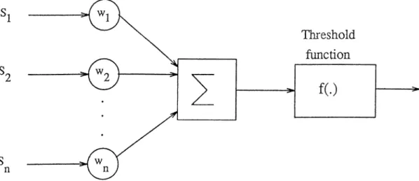
neural systems arises irorn the collective behavior of manj' primitive, highly interconnected processing units. Therefore, artificial neural networks can be characterized by their degree of connectivity. Hopfield’s networks [3] intercon nect fully. A feedback process connects the output of each neuron to the input of each other neuron. In Rumelhart’s multila3'er Perceptrons [4], the output of each neuron connects to all neurons in the next la3'’er. In locally intercon nected networks like Cellular Neural Networks, every neuron is connected to the nearest neurons in a neighborhood. In each of these three models, the functionality of neurons (processing elements) and synapses (interconnection elements) is roughly equal. An artificial neuron performs the weighted
summa-1 1 -1 Hard Limiter
(a)
Piece-wise Linear (b) Sigmoid(c)
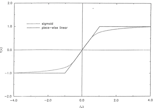
Figure 1.2: Nonlinear neuronal functions : hard limiter (a), piecewise linear (b) and sigmoid (c).
tion of its inputs as shown in Fig.1.1. The result of this summation proceeds through a threshold function. Fig. 1.2 shows three common types of nonlinear threshold functions; hard limiter, piecewise linear and sigmoid. The function of a synapse is to perform a simple multiplication between the output value
CHAPTER 1. INTRODUCTION
of the connected neuron and the weight coeiBcient Wi which may be a positive (called excitatory) or a negative (called inhibitory) real number.
One of the most important aspects of neural networks is their learning ca pability, whereby synaptic weights between neurons are adaptively changed according to a learning procedure. Networks trained with supervision such as Hoplreld and Perceptrons are used as associative memories or as classifiers. These nets provided with side information or labels that specify the correct class for new input patterns during training. ANNs trained without supervi sion, such as the Kohonen’s feature-map forming nets [5] are used as vector quantizers or to form clusters. No information concerning the correct class is provided to these nets during training.
1.2
V L SI C ircuits For N eu ra l N etw ork s
Simulations performed on classical computers account for most of the actual research in artificial neural networks in recent years. However speed looses its importance in simulations because they are much slower intrinsically than electronic devices. Since effective simulations of neural networks exceed the limits of conventional machines, researchers have been working on analog and digital VLSI implementations of neural networks which take the advantage of the inherent parallelism to yield fast solutions. Moreover the integrated neural networks are needed for decentralized mobile systems, robotics and automotive applications in the expanding area of microelectronics.
Neural network models have highly parallel, regular and modular architec tures based on matrices that make them attractive for VLSI s3'stems [6, 7, 15]. Due to the placing and routing problems in silicon wires occupy the most space on an integrated circuit and high-performance interconnections limit the possible number of integrated processing units. Furthermore, cominuniccv tion delays degrade the performance, becoming progressively more expensive in silicon area and propagation time. Therefore, a successful integration of neural network should exhibit the following architectural properties :
• design simplicity that lead to an architecture based on copies of a few simple cells and simple chips;
• regularity of the communication structure that reduces wiring problems and localized communications;
CHAPTER 1. INTRODUCTION
• expandibility and design scalability that allow many identical units by packing a number of neurons onto a chip and interconnecting many chips for a complete system.
In the implementation of neural networks, the weighted summation of input signals (activation function) incurs the largest computational load. A digital implementation serially calculates this sum and requires a data bus for each ¡processing unit. The bus must have the width proportional to the data format of the weights and inputs. As a consequence, the summation must be syn chronous but it gives a high precision and noise immunity. In analog case the weighted sum of the inputs is performed by summing the analog currents or charge packets. A conventional operational amplifier (the simplest circuit is an inverter or an analog comparator) can perform the transfer function. Analog implementation is fast and requires less silicon area than digital implementa tions.
The second critical task is the implementation of connection element. The design of interconnection elements must balance the cell size and the resolution of the connection weight. The implementation of digital memories are well mastered techniques and storage in analog memories is difficult. Proposals for analog synapses include capacitors, charge-coupled devices (CCDs) and MNOS/CCD (metal nitride oxide silicon) circuits [8].
Learning or self-organization does require incremental adjustment of the weights in small steps. In general, such a connection element requires consid erable circuitry, and hence a large amount of silicon area especially in the case of digital weights. Therefore analog circuits are most appropriate for learning algorithms with high fault-tolerance and requiring moderate or low precision, while digital circuits are used for high-resolution learning algorithms.
Optoelectronics can offer a solution to the adaptation and high data rate problems in neural networks by integrating light waveguides and photo diodes into silicon [9, 10].
1.3
M o tiv a tio n and A pproach
A Cellular Neural Network (CNN) as proposed by Chua and Yang, is a spe cial type of analog nonlinear processor array. Due to their continuous-time dynamics and parallel processing features, analog CNN circuits are very ef fective in real time image processing applications such as noise removal, edge
CHAPTER 1. INTRODUCTION
detection and feature extraction [11]. The regularity, the parallelism and the local connectivity found in CNN circuits architecture make it suitable for VLSI implement ations.
This work presents the implementation of cellular neural network structure using analog CMOS circuits. One of our major goals is design simplicity. To achieve this, the design is reduced to CMOS transconductance elements. One can easily adapt this realization to various types of applications by just choosing the appropriate transconductance parameters according to the predetermined coupling coefficients between the neighboring cells. These coefficients may be either set according to a computer simulation or· chosen based on prominent kernels for image processing.
Another important reason for using CMOS transconductance elements is the requirement of adaptability. To achieve programmable coupling coeffi cient, the transconductance parameters can be adjusted with external voltage sources.
In the implementation of “fix function” cellular neural networks that per forms one or a related set of processing function using fixed coefficients, the number of transistors is reduced further by a new m ulti-input voltage-controlled current source.
C hapter 2
C ellular N eu ral N etw orks
A novel class of information processing system called Cellular Neural Network (CNN), ¡possesses some of the key features of neural networks like asynchronous parallel processing, continuous-time dynamics and global interaction of net work elements. They have important potential applications in such areas as image processing and pattern recognition [12]. In this chapter we will briefly review the architecture, stability and applications of CNN proposed by Chua et.al.
2.1
A rc h itectu re o f C ellular N eu ra l N etw ork
In a cellular neural network structure, the basic circuit unit called cell, is interconnected directly to the nearest cells in a neighborhood. The cells which are not directly connected together maj' effect each other indirectly because of the propagation effects of the continuous-time djmamics. An example of
M X N cellular neural network structure is shown in Fig. 2.1. The ith row and
j t h column cell is indicated as C{i,j). The r- neighborhood Nr of radius r of
cell C{i,j) in ei M x N cellular neural network is defined by :
N r{i J ) — {C{k,l)\max{\k - i\,\l - j\} < r, l < k < N (2.1) where r is an positive integer number.
The principle circuit model of cell C{i,j) is shown in Fig. 2.2, where the suffixes u,x and y denote the input, state and output, respectively. It is con structed from linear and nonlinear dependent sources, linear resistors and a linear capacitor.
CHAPTER 2. CELLULAR NEURAL NETWORKS
I
I
I
(c (M ^ --- (c (A ^
Figure 2.1: M x N Cellular Neural Network Structure.
V ··uij V ··
xij Vyij
CHAPTER 2. CELLULAR NEURAL NETWORKS
The node voltage Vuij is called the input of the cell C{i,j) and is assumed to be a constant with magnitude less than or equal to 1. The node voltage v^ij of C{i,j) is defined as the state of the cell whose initial condition is assumed to be a constant with magnitude less than or equal to 1. Finalty, the node voltage Vyij is defined as the output.
Ixu and Ixy are the voltage-controlled current sources which are coupled to
its neighboring cells via the input v^ikt and the output Vyki of each neighbor cell
C(k, 1) with the characteristics
and
^xv.{LJ)k,l^ — B(^i, j] k, I'jVnki
j ^k^V^ Ai^i ^ J 1 k ^ l^Vykl
(2.2)
(2.3) Therefore, the input control and the output feedback of the CNN architecture depend on the transconductances k, 1) and A { i J \ k, /), respectively. The
nonlinear output voltage-controlled current source Iyx{i,j) character istic
(2-4) where /(·) is either a piece-wise linear or a sigmoid type of function as shown in Fig. 2.3. / is the biasing current and Eij is the constant input voltage.
By applying KirchhoiF’s current and voltage laws, the circuit equations of a cell in an iV x M CNN can be easily derived as follows:
State equation: C at
T 'y ] j] k.1
l^Vyki{t)-\-+ ^ B(i,j]k,l)vuki + 1 (2.5)
Input and Output equations : - Eij J ~ (^ ) ) (2.6)
Constraint conditions: (2.7)
Parameter assumption: J J ) ^5 0 “ “^(^5 ^ ) J ) (2.8) where 1 < i , k < M; 1 < j , l < N.
In practice, the magnitude of the signals can always be normalized to satisfy the constraint conditions and the parameter assumption is reasonable because of the symmetry property of the neighborhood system.
CHAPTER 2, CELLULAR NEURAL NETWORKS
- 4 .0 - 2.0 0.0
(v)
2.0
Figure 2.3: The nonlinear characteristics of /(·)·
2.2
S ta b ility
4.0
In order to determine the dynamic range of all node voltages in the network, it is proven that, the state Vxij of each cell in a CNN is bounded for all time
t > 0 and the bound Vmax can be computed by the following formula for any
CNN [11] :
'^max —- l + R^\I\ + Rj; \<t<M, 1<]<N max [ _ f-—<Y ] {\A{i,j-,k,l)\ + \B{iJ-,k,l)\)]
C(ij)6NrO-,i)
(2.9) For any CNN, the parameters R^, C, I, A{i,j;k, /) and B { iJ ] k, 1) are finite constants, therefore the bound on the states of the cells, Vmax, is finite and can be computed via formula (2.9).
In stability analysis, it can be easily proven that [11], every cell output has two equilibrium points ( i l ) . Therefore, after the transient has settled down, a CNN alwajfs approaches one of its equilibrium points. In other words.
or
lim Vxij{t) = constant] l < j < N t-^OO
lim = 0
t—¥oo dt
(2.10)
CHAPTER 2. CELLULAR NEURAL NETWORKS 10
Moreover if the circuits parameters satisfy
then or equivalently, 3 ) 0 ^ n ■TCx lim \v:cij\ > 1 t—fOO lim Vyijit) = ±1. t—^oo
(
2.
12)
(2.13) (2.14)The equation (2.14) is significant for cellular neural networks, because it implies that the circuit will not oscillate or become chaotic. This equation also guarantees that CNN converges to a binary value output which is a crucial property for solving classification problems in image processing applications.
2.3
A p p lication to Im age P ro cessin g
In order to understand the image transform mechanism in cellular neural net works, let us rewrite the state ec[uation (2.5) in its equivalent integral form as follows:
-'XIJ
where
and
(i) = u^,-y(0) + ^ f [-^Vxij{T] + /¿j(r) -b gij{T) + I]dr (2.15)
^ Jo
A{i,r,k,l)vyM{t) (2.16)
<?>i(0 = Y B{iJ;kJ)vuki (2.17)
Equation (2.15) represents the image at time t, which depends on the initial image Ua;ij(0) and the dynamic rules of a cellular neural network. Therefore, cellular neural networks can be used to obtain a dynamic transform of an initial image at any time t. In special case t oo, the state variable Vxij{i) tends to constant and the output Vyijft) tends to either -fl or —1 as stated in equation (2.14).
The result of this dynamic transform depends on the choice of the cell equiv alent circuit element values, i.e. transconductance of linear current sources
CHAPTER 2. CELLULAR NEURAL NETWORKS 11
{A{i,j', k, 1) and k, /)), the bias current (/), the resistances (R^ and Ry),
capacitance C and the radius of the direct interactions between cells (r). El ements mentioned above are called CNN parameters and how to choose these parameters to achieve a desired transformation is currently still an active re search problem [25], [26]. Some application possibilities like noise-reduction and edge detection are mentioned in Chapter 4, and others can be found in the references [12],[17]-[20].
C hapter 3
A nalog CM OS Im p lem en ta tio n o f C N N
3.1
CM OS T ran scon du ctan ce E lem en t
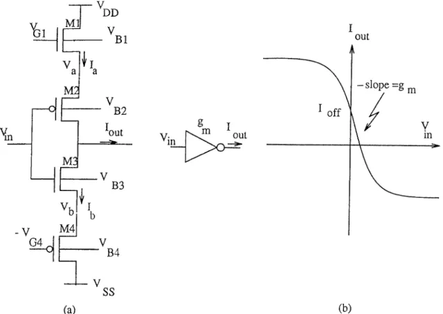
The linear CMOS transconductance element (voltage-to-current transducer) which is shown in Fig. 3.1.(a), resembles in most respects that of the CMOS inverter but without the matching problems between PMOS and NMOS tran sistors and with the additional advantage of tunability [21]. In this section, DC operation of this CMOS transconductance element is analyzed and some SPICE simulations are shown to demonstrate the performance.
In DC anal}'^sis of the linear region defined in Fig. 3.1.(b), using the stan dard square-law model for MOS in their saturation region and assuming a per fect matching between the geometrically identical NMOS transistors M l , M2
and between PMOS devices M2, M 4, the currents la and ly defined in Fig. 3.1.(a) are easily derived as
/ . = Kit(Vat - Vin - Vm, - \VtA Y h = k„j(Vo, + - 1/t„3 - \VTrA\f (3.1) (3.2) where
,
_
kp
' {-\/kn + \/^í>)^ 1 W ^n,p = jCox{-j-y)n,pand Vtux > 0) ^Tpi < 0. These parameters have their usual meanings.
(3.3)
(3.4)
CHAPTER 3. ANALOG CMOS IMPLEMENTATION OF CNN 13 V Ml
G1
V DD V B1 out M3Xn
V M3 B2 out V M4 G4 B3 B4 SS (a) (b)Figure 3.1: The transistor schematic (a) and the input-output characteristic (b) of CMOS transconductance element.
Thus with equations 3.1 and 3.2, the output current Rut = la — h equals lout ~ 9 m ^ in P I-off
where the abbreviations
9m — '^ k e fj[V a i + Vg4 — ( y T n l + 14’n3 + |^ p 2 | + |b'rp4|)] (3.6)
^ofj ~ ^[ {Vx nz - Vtui) + (|^p4| - iVrpzl) + (Vgi - Va-i)] (3.7)
are introduced for the transconductance parameter and the offset current, re spectively.
Although the offset current lojj is not equal to zero due to the body effect, it can be easily eliminated by an appropriate setting of Vba in an n-v^ell process
and Vbi in a p-well process for Vox — Vg4 = Vq and Vb2 = K where Va is a node voltage as defined in Fig. 3.1.
For linear operation of the transconductance element, all the transistors must stay in their saturation region, as was assumed in the derivation of (3.5), i.e. the conditions Vd s>Vgs - Vrn for n-channel and Vs d^ Vsg ~ ll-^pl for
CHAPTER 3. ANALOG CMOS IMPLEMENTATION OF CNN 14
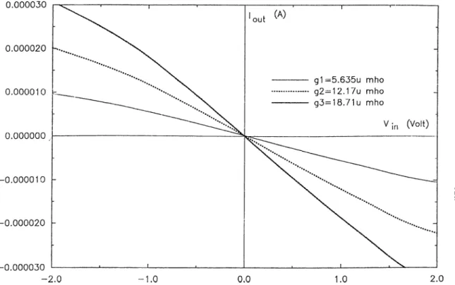
Figure 3 2; Simulation results of the transconductance element : {WlL)n — 0.38, ( W / L ) , = 0.29 for = 0.77, {W/L), = 0.57 for 92 and
{W/L)n = 1.15, {W/L)t, = 0.85 for 93.
p—channel transistors must be satisfied. This leads the requirements
- |% 2 l < ( V '„ - r „ ,) < '^ r » 3 (3-8) — Vrnl. r s s < — Vg4 + |rrp4| (3-9)
in addition to
- Vg4 + Vxn3 + \Vxv‘i\<Vin<yGl - ^Tnl - |Vrp2| (3.10)
SPICE simulation results for different values of transconductace parame- ters, using 1.5-/^ SPICE model parameters are shown in Fig. 3.2. In these simulations Vbi == Pss — Vs s^Vgi ~ — 3.5V^ and bulk voltage Vba is chosen appropriately to eliminate the offset current defined in equation (3.7).
CHAPTER 3. ANALOG CMOS IMPLEMENTATION OF CNN 15
N
gx1
Syx cFigure 3.3: The cell circuit realization with CMO.S transducers.
3.2
R ealization o f a C ell w ith CM OS T ransconduc
tances
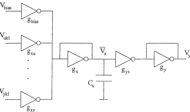
Because of its simplicity, the CMOS transconductance element is chosen as the basic building block for the integrated circuit realization of the cell circuit. The circuit diagram of the integrated circuit realization of one CNN cell with CMOS transconductance element is shown in Fig. 3.3. It consists of the summation node, where all the input currents and the bias current are summed, the state and output resistors, the input and output voltage-controlled current sources and the sigmoid function.
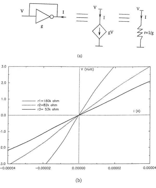
The main problem in VLSI circuits is the implementation of the resistors that are not commonly used in standard CMOS technology. They usually occupy a large chip area which makes it impossible to implement networks with huge number of resistors. In order to eliminate this problem, we have implemented the cell circuit resistors and Ry defined in Fig. 2.2, by sim ply connecting the input of the transconductance to its output as shown in Fig. 3.4.(a). The desired resistance values can be easily achieved by choosing the appropriate transconductance parameters. SPICE simulation results for different resistance values are shown in Fig. 3.4.(b).
CHAPTER 3. ANALOG CMOS IMPLEMENTATION OF CNN 16
V _
V I
r=Vg
(a)
Figure 3.4; The circuit diagram (a) and the characteristic (b) of a CMOS resistor for different resistance values.
CHAPTER 3. ANALOG CMOS IMPLEMENTATION OF CNN 17
Figure 3.5: Output nonlinearity with CMOS transconductance elements.
V
in I out — m^
g
Figure 3.6: Inhibitory coupling coefficients with CMOS transconductance ele ments.
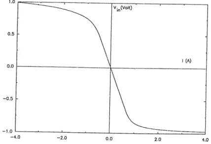
The sigmoid type nonlinear transformation, needed at the output of the cell circuit, is performed with two transconductance element as shown in Fig. 3.5. The second transconductance element whose input is connected to its output, acts like the resistor Ry and the output voltage Vy drives individual current sources whose outputs are coupled to the neighbors.
Fig. 3.2 shows the linear behavior of the transconductance parameter for lKn| ^ IvoH. Since input voltages v^ij and the output voltages Vyij are bounded with Ivolt, the input control and the output feedback A(i,j-,kJ) voltage-controlled current sources are obtained by using the transconductance elements in their linear region.
The desired coupling coefficient can be easily achieved by simply choosing the appropriate transconductance parameters. The negative (inhibitory) cou pling coefficients can be obtained by inverting the positive (excitatory) input with a cascaded transconductance element pair as shown in Fig. 3.6.
CHAPTER 3. ANALOG CMOS IMPLEMENTATION OF CNN 18
realization shown in Fig. 3.3 satisfies the same state equation (2.5);
J 5 ^ ) 0 — ^ x y i } ) 3 ! 0 (3,11) j ( z j j j ¿ 5 / ) (3.12) R x i j — Qx-i j (3.13) R y i j — 9 y i ] (3.14) ^ — Q b i a s ^ ^ b i a s (3.15) ' ^ x i j — ~ V x i j (3.16)
In order to periorrn one or a related set of processing functions using fixed coefficients, the transconductance parameter varicition can be achieved choosing the gate-width-to-gate-length ratio {W/L) a p p ro p riate!after setting Vgi = Vdd = 5F and - V o i = = —51/.
3.3
P rogram m ab le C oupling C oefficien ts
The requirement of adaptabilit}' is difficult to achieve in most neural network VLSI implementations [13],[22]. In the realization of the CNN structure with CMOS transconductance elements, we can achieve a programmable imple mentation by varying the transconductance parameters with external voltage sources connected to the gate voltages Vq\ and Voi of each cell defined in
equation (3.6). SPICE simulation results of the transconductance parameter variation for different gate voltages is shown in Fig. 3.7. But one of the ma jor problems in VLSI programmable implementations of CNN is the wiring needed for changing the template coefficients of each cell. Since all the cells of a cellular neural network have the same coupling coefficients A{i,j·, k, 1) and
k, /), the wiring problem can be reduced by controlling the transconduc
tance parameter variation of all cells with the same set of external voltages as shown in Fig. 3.8
CHAPTER 3. ANALOG CMOS IMPLEMENTATION OF CNN 19
Figure 3.7; Simulation results of the transconductance parameter variation.
Figure 3.8: Programmable 4x4 CNN structure using CMOS transconductance elements.
CHAPTER 3. ANALOG CMOS IMPLEMENTATION OF CNN 20
V
On
V
mFigure 3.9; M -input voltage-controlled current source.
3.4
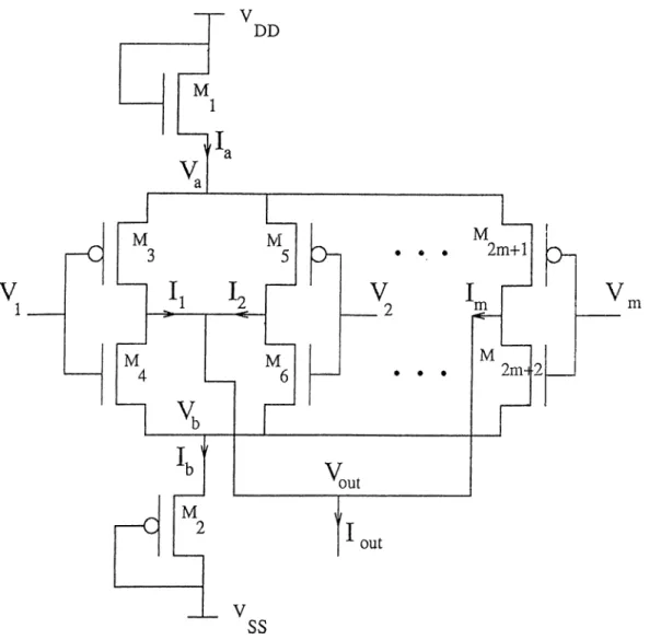
R ed u ced H ardw are
In order to decrease the number of transistors in the realization of cellular neural network structure, we have presented a new type of multi-input voltage- controlled current source (VCCS) which is shown in Fig. 3.9. This m ulti-input VCCS is similar to m transconductance elements with common output, except upper NMOS and lower PMOS transistors are common.
In DC analysis of this new m -input voltage-controlled current source, as suming matching between NMOS transistor M l and PMOS transistor M2 and using the standard square-law model for MOS transistors in their saturation region, the current lout can be derived as
771
^out — [ 9eff / ^ K' A] (3.17)
CHAPTER 3. ANALOG CMOS IMPLEMENTATION OF CNN 21 where Iç 9 e j j = -^[VdD - Vss - V r n l - \Vtp2\ ~ X ) FTp(2i+l) | + VTn{2i+7))] (3.18) 9 e f f ^ o ff = - ^ [ V dD -I- - VtuI + \Vtp2\ - ^.W i{ \V T p (2 i+ l)\ ~ 1^rn(2.+2))] (3.19) A = [- VdD + VTnl + Y^iWi{Vi + |Vrpî;|)]^[[-l'^55 - |Vrp2 + Y^iWi{Vi - 14 m)]^ (3.20) The conditions that should be satisfied in the derivation of equation (3.17) are t> _ U _ U _ ^?i(2i+2) _ ^'p{2i-\-\) ^ _ 1 r) fQ oi ^ ^ — ^nl — '''p2 — — --- Î — 1) 2, 0, ..., Î7Z. lo.21 j Wi Wi and Wj - 1 and Wi > 0.; (3.22)
¿=1
where and kpj are the NMOS and j'* PMOS transistor parameters which are defined in equation (3.4), u;,’s are the scaling factors and m is the number of input voltages.
The inhibitory coupling coefficients can be obtained by inverting the posi tive (excitatory) input with a cascaded transconductance element pair shown in Fig. 3.5. It can be easily shown that, the maximum of the A term defined in equation (3.20) is less then 0.015, that is
max percentage error < 1.5%. (3.23) The derivations of the output current and maximum percentage error are given in Appendix A.
Since the maximum error is less the 1.5%, this m ulti-input VCCS can also be used in the implementation of fixed function CNN structures. SPICE simulation results for two-input VCCS which defines the plane
^out — gejf{wiVi -b W2V2) + loff
is shown in Fig. 3.10.
To obtain a perfect matching between and kp2 is a difficult task to achieve in practice, since the electron and hole mobilities fin and fip depend
CHAPTER 3. ANALOG CMOS IMPLEMENTATION OF CNN 29.
CHAPTER 3. ANALOG CMOS IMPLEMENTATION OF CNN 23
on doping, bias voltages and temperatures. Therefore, to see the effects of mismatching between kni and kp2 on this new multi-input voltage-controlled current source, a SPICE simulation for the case = 0.75kp2 is performed and the result, that is shown in Fig. 3.11, again has defined a plane similar to the previous one (Fig. 3.10) showing that matching between and kp2 is a tolerable requirement.
C h apter 4
Sim ulations
One of the important problems in image processing is image segmentation. In image segmentation, each pixel of the image is classihed into two or more classes. From the mathematical point of view, pixel classification can be con sidered as a map F, which maps a continuous vector space into a discrete vector space as defined below:
F : [a, 6]Mx N Mx N (4.1)
where M x N is the number of pixels in an image and A , B , C , . . stand for different classes. For cellular neural network applications, we wish to assign to each pixel in the array one of the two values —1 and 1 based on some classification rules and the original pixel values. So F is defined by
i ’ : 1-1.1)Mx N { -1.1}Mx N (4.2)
In the following sections, some examples of this kind of image transform performed by our analog CMOS realizations of cellular neural networks is pre sented. In the simulations of these networks, the circuit simulator SPICE2g6 is used. We have developed a preprocessor software called “cnn2spice” to gener ate the input circuit files for SPICE2g6 automatically. This program generates
N X M CNN circuit file according to the predefined cell circuit and the input
images are presented to the network as a set of initial conditions to the state capacitors. We have also developed two postprocessors, called “spice2plot” and “plot”, which map the standard outputs of SPICE2g6 between 0 and 255 uniformly and then feed them to a color graphics terminal as gray level images.
CHAPTER 4. SIMULATIONS 25
In our CNN implementations, a large state capacitor value of lOpF is chosen in order to dominate the d3mamics of the cell. Although this ma}' slow the cir cuit down somewhat (most of the simulations have settling time about 4/isec), it makes the circuit less sensitive to parasitic capacitances and resistances that can occur in any fabricated circuit.
In 12x12 noise-removing and 8x8 edge detection CNN circuit simulations, in order to reduce the memory requirement by computer, the four-transistor transconductance elements was first simulated using 1.5-p SPICE model pa rameters and then its characteristics was modeled with 10'^ order polynomials by minimizing the sum of squared deviations [23]. Finally, the simulation of the CNN architecture is performed using these lO^^"· order polynomials as nonlinear voltage-controlled current sources in the SPICE input file.
4.1
Line D e tectio n
Although line detection is a very simple example image processing problem, it gives some intuitive ideas on how to design a Cellular Neural Network for solving a practical image processing problem.
For the “horizontal line detector” circuit, a very simple dynamic rule is chosen. The circuit element parameters of the cell C{i,j) are as follows :
C = lOpF, 7 = 0, = 1801-0, 1, /) = 0,
A { i , j , i - l , i - 1) = A { i,j ,i - 1,;) = A { i J , i - l , j + 1) = 0, A { i , j , i , j - 1 ) = 9x, A { i , j , i , j ) = 2g^, A { i J , i , j + l ) = g x ,
A ( i , j , i + l , j - 1) = A ( i , j , i + I J ) = A { i J , i + l , j -1-1) = 0. (4.3)
for a 3 X 3 neighborhood system. The feedback operator A { i,j ,k .l ) are space
invariant, that is A{i,j, k, 1) = A{i - k , j - /), therefore as in image processing filters, we can use a cloning template matrix to describe the feedback operator of the cell as follows :
(4.4) 0 0 0
9x 2.gx 9x
CHAPTER 4. SIMULATIONS 26
where the center entry of the cloning template correspond to A(i,j,i,j)·, the upper left corner entry correspond to A { i , j , i - l , j - 1 ) and so forth. Since it is extremely convenient and clear to characterize the interactions of a cell with its neighbors by means of a cloning template matrix, we will use the cloning- template matrix expressions in the following sections.
The dynamic equations of the cellular neural network corresponding to the above parameters are given by:
í7j. and
foi' 1<*<4, l< i< 4 where /(·) is a sigmoid type nonlinear function. The condition
(4.5)
(4.6)
A { iJ - , kJ ) > Rx
defined in Equation (2.12) is satisfied.
From the circuit Equations (4.5) and (4.6), it can be easily seen that the derivative of the pixel values depends on their left and right neighbors, but not on the upper and lower neighbors. This particular dynamic rule will therefore enhance the detection of horizontal lines in the original image.
As mentioned before, every cell in a Cellular Neural Network has the same connections as its neighbors. Therefore, the circuit equation of each cell is the same as those of the other cells in the same circuit. (Without loss of generality, the boundary effects are ignored). Hence, we can Understand the global properties of a cellular neural network by studying the local properties of a single cell. This approach is extremely useful for analysis and design of cellular neural networks.
With the circuit parameters defined in Equation (4..3), a 4 x 4 cellular neural network is simulated using 1.5-/Í model card in SPICE2g6 at the transistor level. From the first simulation results of this simple example, that is shown in Fig. 4.1, it can be easily seen that the row 3 stands as a black horizontal line with value 1.0 and flanked by white background with value —1.0. Hence the circuit is capable of extracting the horizontal lines in the given image in
CHAPTER 4. SIMULATIONS 27
upper left corner of Fig. 4.1. This simple example have shown that, CNN circuits can recognize and extract some special patterns from input images, by choosing the circuit parameters (i.e., the dynamic rule) appropriately.
original im age initial condition t=0 t= 0.25u sec
t= 0.50u sec f"' Sir'' i'
t= 0.75u sec t= 1.25u sec
t= 1.50u sec t= 1.75u sec t= 2.00u sec
CHAPTER 4. SIMULATIONS 28
4.2
N o ise R ed u ctio n
One of the well-known techniques to reduce noise from the image is to use an averaging operator which corresponds to a lowpass filtering [12], [24]. There fore, the averaging operator is chosen as the feedback operator of the noise- reducing cellular neural network. The circuit parameters of our implementation for 12 X 12 noise-reducing CNN are chosen as follows:
0 9x 0
9x 2-(jx 9x ; 5 = 0; / = 0; 5^. = 180A-.Q; C = 10p5; (4.7)
0 9x 0
A =
and the resulting cell circuit equations for the are given by
dVxijlt') Qx . , , .
-f- 2vyij(^t') -f- Vyij^i(tj -fi
Vyijit) = f{vxij{t)) for 1<K 12, l < i < 12 (4.8)
Since the rate of change of the state of cell C{i,j) is cipproximately propor tional to the average of the outputs of the neighborhood Ni {i,j), the steady state of C ( i , j) depends on the average of those of its neighbor cells.
With the circuit parameters defined in equation (4.7), a 12 x 12 noise- removing cellular neural network circuit is simulated using the circuit simula tor SPICE2g6. Figures 4.2, 4.3 and 4.4 show the three simulation results of 12 X 12 noise-removing cellular neural network circuit. In these figures, the
noisy input images are defined at the upper left part and the rest of the pic tures are the outputs at different time steps. This CNN circuit has the same properties as a two-dimensional low-pass filter. It retains the low-frequency components while eliminating the high-frequency components. In the spec trum of an image, the high frequency components contain information about the corners of objects. These high-frequency components are removed along with the high-frequency noise because of the low-pass filter effect. Therefore, the pixel classification is not always correct at the corners of the objects as seen in the Fig. 4.3.
CHAPTER 4. SIMULATIONS 29
CHAPTER 4. SIMULATIONS 30
CHAPTER 4. SIMULATIONS 31
original im age initial condition t=0 t= 0.25u sec
...«
t= 0 .7 5u sec t= 1.25u sec t= 1.75u sec
t= 2 .2 5u sec t= 2.75u sec t= 3.25u sec
CHAPTER 4. SIMULATIONS 32
To see the dynamic behavior of the circuit in more detail, the output tran sient characteristics of cells (7(1,7), C (7 ,2) and C(8,2) are displayed in Fig. 4.5. These transient characteristics which are taken from the simulation results in Fig. 4.2, shows that the cell outputs reach their appropriate stead}'· state values depending on both their neighbor cells and initial conditions.
From the simulation results, it can be seen that cellular neural network circuit defined with the circuit parameters in equation (4.7) is elFective for removing noise in image processing, especially for images with large objects and few corners as in Fig. 4.4.
CHAPTER 4. SIMULATIONS 33
4.3
E dge D e te c tio n
In this application, we have used another two-dimensional filter called Lapla-
cian operator as the feedback operator to detect the edges of a square. The
circuit parameters for this 8 x 8 cellular neural network circuit is defined below
A =
and
0 9x 0 -9x 4(/.T -9x
0 -9 x 0
5 - 0 ; / - 8/iA; Rx = ISOW.] C = lOpF;
(4.9)
dvxij (¿)
dt C
1 ( 0 "h 4 u y ,' j ( i ) y y j j .j .i ( i )
% d(0 = l < i < 8 (4.10) The result of the circuit simulation is shown in Fig. 4.6. The parameter I in this example can control the derivatives of the state variables, and thus affects the dynamics of the circuit.
CHAPTER 4. SIMULATIONS 34
t=0 t= 0 .1 25u sec t= 0.25u sec
t= 0 .3 75u sec t= 0.5u sec t= 0.75u sec
t= 1 .2 5u sec t= 2.25u sec t= 2.5u sec
C h ap ter 5
C on clu sion
An analog CMOS circuit implementation of cellular neural network has been realized and some applications in image processing are presented. These ap plications show that cellular neural network implementation proposed here, can be used as a two-dimensional filter. Moreover, its parallel processing and continuous time features make it possible to process large-size images in real time. The estimated chip area for a 20 x 20-neuron CNN is about i m m x 4mm using 1.5/i CMOS technology.
The design of CNN circuits is reduced to a transconductance element and it can be easily adapted to various tyj^es of applications bj^^ just tuning the cip- propriate transconductance elements according to the predetermined coupling coefficients between the neighboring cells as it is performed in noise-removing and edge detection examples.
The realization of CNN with CMOS transconductance elements can be either programmable or fix function. In order to reduce the wiring problems in programmable CNN circuits, the desired coupling coefficients can be achieved by changing the transconductance parameters of each cell circuit with the same set of external voltage sources. In fix function CNN implementations, the number of transistors are reduced further by introducing a nev.’ multi-input voltage-controlled current source.
This analog CMOS realization of Cellular Neural Network can be integrated by optoelectronic sensors and/or charge-coupled devices to feed the input pat tern to the neural processors.
A p p en d ix A
D erivation s o f M u lti—Inpu t V C C S
For the m -input voltage-controlled current source that shown in Fig. 3.9, let
k = kni = k,2 = i = l, 2,3,..., m. (A.l) W i l O i and m ^ ^ Wi = 1 and Wi > 0 .; 1=1
ith ATA,friQ ni/i
(A.2) where and kpj are the NMOS and PMOS transistor parameters which are defined in equation (3.4), ru,’s are the scaling factors and m is the number of input voltages.
In DC analysis, using the standard square-law model for MOS tra.nsistors in their saturation region, the currents la and /b, defined in Fig. 3.9, are easily derived as and where and (A.3) k S n (A.4)
^ = - VdD + VttiI + + I^H(2t+l)|) (A.5)
V = -^'^55 — \yTp'¿\ + “ ^n(2i’+2)) (A.6)
m m
S = ^ WiV^ - WiVil'^ (A.7)
1=1 1=1
APPENDIX A. DERIVATIONS OF MULTI-INPUT VCCS 37
Thus with equations (A.3) and (A.4), the output current Rut = la - h equals
I ^ , = j [ ( i + - (>) + - ) ’l (A.8) which implies where lout — [ 9 t j j ^ ^ WjVj T Ayy][l Z\] i= l (A.9) 9 e f f = - ^ i^ D D - V s s - V x n l - \Vt p2\ ~ ^ 4 ' ^ ! ' ( n 4 ’p ( 2 t + l) | + l'^Tn(2t+2))] \}^DD + V s s — V l ^nl + \Vt p2\ - W i ( \ V T p ( 2 i + l ) \ - VTn{2i+2))] Uji = A = 9e}} 2 6^ (A.IO)
The maximum percentage error can be written as max percentage error = max A x 100
max min X 100 (A .ll) Since |K|<1 and = 1 771 m max = m a x [ ^ WiV^ -t=l ¿=1 = 1
and assuming V T (n ,p )i^lV , Vdd = — Vss = 5V m min|(f7/p = m in[(y^tc’,K’)^ — 9]' ¿=1 = 64 (A.12) (A. 13)
Inserting (A.12) and (A.13) into (A .ll), the rna.ximum percentage error is be obtained as
max percentage error < ^ ^ 199
R eferen ces
[1] D.A. Anderson and E. Rosenfeld, (Eds.), “Neurocomputing”, MIT Press, 1988.
[2] R. Echmiller and C. Maloburg, “ Neural Computers”, Springer-Verlag, 1988.
[3] J. J. Hopfield, “ Neural Networks and Physical Systems with Emergent Col lective Computational Abilities,”Proc. Nat‘l Academy Set., Vol.79, Apr. 1982, pp 554-558.
[4] D. Rumelhart et.ah, “Parallel Distributed Processing”, MIT Press, 1986. [5] T. Kohonen, “ Self-Organization and Associative Memory,”Springer-
Verlag, 1984.
[6] U. Rueckert and K. Goser, “ VLSI Design of Associative Networks,” VLSI
for Artificial Intelligence, Kluwer Academic Publisher, pp227-235,1989.
[7] P. Treleaven, M. Pacheco and M. Vellasco, “VLSI Architectures for Neural NetAvorks”, IEEE Micro, pp.8-27, Dec. 1989.
[8] J.P. Sage, K. Thompson and R.S. Withers, “An Artificial Neural Net work Integrated Circuit Based on MNOS/CCD Principles,” Proc. Neural
Netxuorks for Computing Conf, Vol. 151, pp 381-385, 1986.
[9] D.G. Hall, “ Survey of Silicon-Based Integrated Optics,” Computer, Vol.20, No.l2, pp 26, 1987.
[10] A. Torinmi et.al., “ A Study of Photon Emission from n-channel MOS- FETS,” IEEE Trans, on Electronic Devices, Vol.23, No.12, pp 55-60, 1986. [11] L.O. Chua and L. Yang, “Cellular Neural Networks : Theory”, IEEE
Trans. Circuits Syst., Vol. 35, no.10, pp. 1257-1272 , October 1988.
[12] L.O. Chua and L. Yang, “Cellular Neural Networks : Applications”, IEEE
Trans. Circuits Syst., Vol. 35, no.10, pp. 1273-1290 , October 1988.
REFERENCES 39
[13] L. Yang, L.O. Chua and K.R. Kried, “VLSI Implementation Of Cellular Neural Networks”, Proc. IEEE ISCAS, pp. 2425-2427, 1990.
[14] V. Vemuri,“Artificial Neural Networks”, Computer Societ}^ Press, 1988. - ; [15] II.P. Graf and L.D. Jackel, “Advance in Neural Network Hardware,” Proc.
Int. Electron Devices Meeting., 1988.
[16] C. Mead, “Analog VLSI and Neural Networks,” Addision-Wesley, 1989. [17] T. Matsumoto, T. Yokohama, PI. Suzuki, R. Furukawa, A. Oshimoto, T.
Shirnmi, Y. Matsushita, T. Seo and L.O. Chua, “Several Image Processing Examples by CNN”, Proc. IEEE CNNA, pp. 100-106, 1990.
[18] J. Denker (Ed.), “ Computing with Neural Networks”, American Institute of Ph3'^sics, 1986.
[19] G. Serker, ” Small Object Counting with CNN,Proc. IEEE CNNA, pp. 114-123, 1990.
[20] A. Dzielinski, S. Skoneczng and R. Zbikowski, “CNN Application to MOIRE pattern Filtering”, Proc. IEEE CNNA, pp. 139-148, 1990.
[21] C.S. Park and R. Schaumann, “A High Frequency CMOS Linear Transcon ductance Element,” IEEE Trans. Circuits Syst., Vol. 33, no.11, pp. 1131- 1138, November 1986.
[22] M. Verle3'^sen and P.G.A. Jespers, “An Analog Implementation of Hop- field’s N.N.”, IEEE Micro, pp.46-55, Dec. 1989.
[23] P. Lancaster and K. Salkauskas, “Curve and Surface Fitting”, Academic Press, 1986.
[24] A. Jain, “Fundementals of Digital Image Processing”,Prentice-Hall. [25] F. Zou, S. Schwarz and J.A. Nossek, “Cellular N.N. Design Lsing a Learn
ing Algorithm”, Proc. IEEE CNNA, pp. 73-81, 1990.
[26] K. Slot, “Determination of Cellular N.N. Parameters For Featui'e Detec tion of Two Dimensional Images” , Proc. IEEE CNNA, pp.82-91, 1990.