ISDRS 2009, December 9-11, 2009, College Park, MD, USA
ISDRS 2009 – http://www.ece.umd.edu/ISDRS2009
Gate Bias Characterization of CNT-TFT DNA Sensors
O. Aktasa , T. Toralb
a
Electrical and Electronics Engineering, Bilkent University, Turkey, [email protected] b
Electrical and Electronics Engineering, Bilkent University, Turkey
There have been numerous reports of CNT-TFT DNA sensors in the literature [1-3]. This work follows the approach in references [1,3] that use the change in the current of CNT-TFTs with DNA attachment and DNA hybridization. In this work, we use the back-gated measurement geometry and employ no intercalating agents or Mg salt addition. The aim is to investigate the detailed response characteristics in the full range of CNT-TFT gate bias conditions.
CNT-TFT films were synthesized with thermal chemical vapor deposition technique at atmospheric pressure using methane as the carbon source and ferritin as the catalyst. The growth of the nanotubes followed procedures detailed earlier in the literature [4]. The fabrication of carbon nanotube TFT was done by employing standard photolithography and liftoff processes. As an additional step, the passivation of the source-drain pads against leakage through the DNA solution was achieved by using AZ5214 photoresist. The transistors used for the measurements had a source-drain spacing of 100 μm, a gate-width of 100 μm, and source and drain pad size of 500 μm by 500 μm. The schematic of the structure of the CNT-TFT used in this work is shown in Fig. 1. The measurements of the TFTs were done on a microscope probe station using an HP4142 semiconductor parameter analyzer. During measurements, the CNT-TFT source and drain pads were contacted by tungsten probes by scratching the passivating photoresist film by the tip of the tungsten probe. All measurements were made in a back-gated geometry by contacting the p-type silicon wafer.
For the DNA response tests, 2 μL of 0.1 μM capture probe single strand DNA solution was dropped onto the source-drain spacing area of the transistor and the current-voltage characteristics and transfer characteristics were measured after at least 10 minutes of time. For DNA sensing tests, TNos DNA oligomer was used as the single strand capture probe and target-TNos oligomer was used as the complementary molecule.
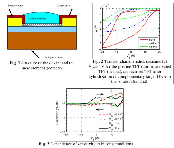
Fig. 2 shows the change in the transfer characteristics of a CNT-TFT with single-strand DNA binding for activation and with complementary DNA binding to activated TFT. From the data in Fig. 2, the normalized sensitivity of the device in the small drain bias regime was calculated using the following formula:
100
*
1
*
C
I
I
I
S
ss ss hyb−
=
where Ihyb is the current after hybridization, Iss is the current after addition of single-strand DNA to the CNT-TFT and C is the concentration of the DNA solution in units of nM. This formula calculates the relative current change normalized with the concentration of the DNA solution and is similar to quantities used in [2] and [5]. With the above definition, the unit for the sensitivity is percent/nanomolar (%/nM). The plots of the sensitivity defined as above are presented in Fig. 3.
For matched DNA hybridization, the measured sensitivity ranges from 0.5 to 0.7 %/nM. This value is similar to previous measurements in the literature. From Fig. 3, it can be seen that the sensitivity is not dependent on the drain bias. However, significantly higher sensitivity is obtained when the gate voltage is being swept from enhancement to cut-off. The increase in sensitivity occurs around the threshold voltage where the sensitivity increases from 0.5 %/nM to 0.7 %/nM. Considering the hysteresis mechanism put forward in [6] it can be argued that the observed increase in sensitivity is due to elimination of screening caused by positive charge carriers injected out from the CNT as the gate bias decreases.
The plots in Figure 2, further show that the passivation of the source-drain pads and the use of a small quantity of DNA solution was effective in eliminating the leakage current through the buffer solution. The elimination of the leakage current through the solution allows us to observe the reduction in metallic CNT current in both the transfer and current-voltage
ISDRS 2009, December 9-11, 2009, College Park, MD, USA
ISDRS 2009 – http://www.ece.umd.edu/ISDRS2009
characteristics. The reduction seen in the metallic CNT leakage current suggests that the metallic CNTs also respond to the attachment of DNA molecules
As a result, we have studied the response of CNT-TFTs to DNA binding and hybridization. We have demonstrated for the first time that an increase in sensitivity is observed around the threshold voltage when sweeping the gate bias from negative to positive values. The results presented in this work suggest an improved approach to measuring the response of CNT-TFTs to DNA hybridization.
The authors acknowledge the kind help of Prof. Dr. H. A. Oktem in supplying the DNA samples. The authors also acknowledge financial support from TUBITAK projects 106E059 and 108E123.
References:
[1] E. Gui, L. J. Li, K. Zhang, Y. Xu, X. Dong, X. Ho, P. S. Lee, J. Kasim, Z. X. Shen, J. A. Rogers and J. Mhaisalkar, “DNA Sensing by Field Effect Transistors Based on Networks of Carbon Nanotubes”, J. Am. Chem. Soc., vol. 129, pp. 14427-14432, 2007.
[2] E. S. Snow, “Chemical Detection with a Single Walled Carbon Nanotube Capacitor”, Science, vol. 307, pp. 1942-1945, 2005.
[3] X. Tang, S. Bansaruntip, N. Nakayama, E. Yenilmez, Y. Chang and Q. Wang, “Carbon Nanotube DNA Sensor and Sensing Mechanism”, Nano Lett., vol. 6, pp. 1632-1636, 2006 [4] H. Dai, “Carbon Nanotubes: Synthesis, Integration and Properties”, Acc. Chem. Res., vol. 35,
pp. 1035-1044, 2002.
[5] S.M. Sze, Ed., “Semiconductor Sensors,” New York, John Wiley and Sons, 1994.
[6] S. Kar, A. Vijayaraghavan, C. Soldano, S. Talapatra, R. Vajtai, O. Nalamasu and P. M. Ajayan, “Quantitative Analysis of Hysteresis in Carbon Nanotube Field-Effect Devices”, Appl. Phys. Lett., vol. 89, p. 132118, 2006.
Back-gate contact Analyte solution
Source contact Drain contact
Fig. 1 Structure of the device and the
measurement geometry
Fig. 2 Transfer characteristics measured at
VDS=-1V for the pristine TFT (norm), activated TFT (ss-dna), and actived TFT after hybridization of complementary target DNA to
the solution (ds-dna).
![Can [F-18] fluorodeoxyglucose positron emission tomography replace sentinel lymph node biopsy for the detection of axillary metastases in patients with early-stage breast cancer?](data:image/gif;base64,R0lGODlhAQABAIAAAP///wAAACH5BAEAAAAALAAAAAABAAEAAAICRAEAOw==)