Soft x-ray photoemission studies of the
system
S. Sayan, E. Garfunkel, and S. SuzerCitation: Appl. Phys. Lett. 80, 2135 (2002); doi: 10.1063/1.1450049 View online: http://dx.doi.org/10.1063/1.1450049
View Table of Contents: http://aip.scitation.org/toc/apl/80/12
Published by the American Institute of Physics
Articles you may be interested in
Band offsets of wide-band-gap oxides and implications for future electronic devices
Journal of Vacuum Science & Technology B: Microelectronics and Nanometer Structures Processing, Measurement, and Phenomena 18, 1785 (2016); 10.1116/1.591472
High-κ gate dielectrics: Current status and materials properties considerations
Journal of Applied Physics 89, 5243 (2001); 10.1063/1.1361065
interface chemistry studied by synchrotron radiation x-ray photoelectron spectroscopy
Applied Physics Letters 81, 3627 (2002); 10.1063/1.1520334
Silicate layer formation at HfO2/SiO2/Si interface determined by x-ray photoelectron spectroscopy and infrared spectroscopy
Journal of Applied Physics 100, 083517 (2006); 10.1063/1.2361161
Oxygen vacancy in monoclinic : A consistent interpretation of trap assisted conduction, direct electron injection, and optical absorption experiments
Applied Physics Letters 89, 262904 (2006); 10.1063/1.2424441
Band alignment issues related to gate stacks
Soft x-ray photoemission studies of the HfO
2Õ
SiO
2Õ
Si system
S. Sayan and E. Garfunkela)Department of Chemistry, Rutgers University, Piscataway, New Jersey 08854 S. Suzer
Department of Chemistry, Bilkent University, 06533 Ankara, Turkey
共Received 8 March 2001; accepted for publication 19 December 2001兲
Soft x-ray photoelectron spectroscopy with synchrotron radiation was employed to study the valence-band offsets for the HfO2/SiO2/Si and HfO2/SiOxNy/Si systems. We obtained a
valence-band offset difference of⫺1.05⫾0.1 eV between HfO2共in HfO2/15 Å SiO2/Si兲 and SiO2 共in 15 Å SiO2/Si兲. There is no measurable difference between the HfO2valence-band maximum
positions of the HfO2/10 Å SiOxNy/Si and HfO2/15 Å SiO2/Si systems. © 2002 American
Institute of Physics. 关DOI: 10.1063/1.1450049兴
The continuous shrinkage of complementary metal– oxide–semiconductor 共CMOS兲 dimensions 共now below 0.1
m兲 to achieve higher performance and integration necessi-tates an increase in gate capacitance while maintaining low leakage current levels. The increased capacitance need is driving extensive research into the use of alternative gate insulators with a higher dielectric constant (k) than that of
SiO2 (k⫽3.9).1,2 The gate dielectric must form a quality low-defect-density interface with silicon. When
high-kmaterials such as ZrO2, HfO2, etc., are bonded directly to
silicon they present higher interface state densities than are observed in the SiO2/Si system. To overcome this problem,
it is preferred to have a few monolayers of SiO2 serving as a
low-defect-density bottom oxide between the high-k
dielec-tric film and the silicon. Although this serves to decrease the interface state density, the capacitance also drops because of the low dielectric constant of SiO2. Another requirement for
any dielectric is that the barrier heights for electron and hole injection should be at least 1 eV 共and preferably larger兲 to have sufficiently low leakage currents. It is, therefore, impor-tant to understand and control the band alignments of alter-native dielectrics on silicon and on SiO2. Photoemission is
one of the most reliable methods to study these systems. Several high-k materials are now being considered as
re-placement dielectrics including HfO2, ZrO2, Y2O3, and La2O3, as well as their silicates and aluminates. In
particu-lar, considerable attention is paid to HfO2 due to its high
dielectric constant (k⫽16– 45), 3,4
high resistivity, and high thermal stability.5
Recently, S. Miyazaki used high-resolution photoemis-sion to study the valence-band offsets as well as work func-tions of ZrO2, Al2O3, and Ta2O5 using total photoelectron
yield spectroscopy.6They calculated the band gaps using the measured band-offset and work-function values. Lucovsky and co-workers studied band offsets for ultrathin SiO2 and Si3N4 films on Si共111兲 and Si共100兲 using soft x-ray
photo-emission spectroscopy 共XPS兲.7 They have found that their spectrum in the valence-band-edge region was well modeled by a pair of Gaussian-broadened Fermi functions. They
ob-tained band offsets of 4.54⫾0.1 eV for SiO2/Si(100) with
film thicknesses in the range of 8 –12 Å. Hattori8studied the SiO2/Si system with different thickness 共5–15 Å兲 regimes
using high-resolution XPS. Both thickness and angle-resolved analytical procedures were used for analysis of the valence-band spectra. During the analysis, it was assumed that the density of states near the valence-band edge follows a parabolic energy dependence. Hattori reported that the top of the valence band of the oxide surface increased by about 0.2 eV near the thickness of 9 Å, which was attributed to oxidation-induced stress in the interfacial transition layer. In this contribution, we report on the valence-band alignments of HfO2/10 Å SiOxNy/Si, HfO2/15 Å SiO2/Si and SiO2/Si
using soft x-ray photoemission.
HfO2 films were deposited using chemical-vapor depo-sition 共CVD兲 employing Hf-t-butoxide as the precursor on different substrates at ⬃400 °C. The substrate used was
p-type Si共100兲 with a doping concentration of ⬃1
⫻1015 cm⫺3. The thickness of the thermal SiO
2 was 15 Å
and that of SiOxNy was 10 Å, as measured by medium
en-ergy ion scattering 共MEIS兲. In the oxynitride, the O:N ratio was ⬃4:1. The soft x-ray measurements were performed at Brookhaven National Laboratories 共BNL兲 on the U8B line using 120– 400 eV photon energies. The spectra at the valence-band edges were modeled by Boltzmann-broadened step functions. We employed several methods to determine the valence-band edge.
The growth, materials, and dielectric properties of the films used in this study are described in more detail elsewhere.10 The dielectric constant of the HfO2 thin films
with Pt electrodes used here was determined to be⬃26 after plotting the optical thickness of a series of HfO2 films of
different thicknesses on the 10 Å SiOxNy/Si substrate versus the electrical thickness as determined by the capacitances at accumulation. The leakage current densities were determined at 1 V beyond the flatband voltage in the inversion regime and found to be on the order of ⬃10⫺7 A/cm2 for the thin-nest sample (tqm⫽11.6 Å).
We modeled the spectra at the valence-band edges by Boltzmann-broadened step functions. Different fitting func-tions and simple smoothing of the data do not measurably change the results; what is important is to have an accurate a兲Electronic mail: [email protected]
APPLIED PHYSICS LETTERS VOLUME 80, NUMBER 12 25 MARCH 2002
2135
fit to the data in the high-energy-tail region 共closest to the Fermi energy兲. Different methods have been reported to de-termine the ‘‘valence-band edge.’’ One method共M1兲 defines an energy based on the energy at the inflection point of a ‘‘best-fit’’ function. Another method共M2兲 employs a ‘‘best’’ straight-line fit to represent the decay in valence-band pho-toemission, and the point of intersection of this line with the base line is taken to be the valence-band edge6 共a related method combining M1 and M2 takes the tangent from the inflection point兲. We also present a third method 共M3兲, some-what similar to the one used in Ref. 7. The idea is to take as the energy edge the point where the signal rises above the base line by a certain fraction or percentage 共e.g. 1–3%兲 indicating a measurable density of states. As we have no a
priori knowledge of the electronic structure at the top of the
valence band 共the precise band structure is unknown, and even the similar ZrO2 case is quite complex兲, nor any
spe-cific knowledge about a possible contribution from interface or defect states, this third method might be more appropriate in determining the electrical properties which rely on a knowledge of the experimental barrier heights共valence-band edges兲. It may be argued that a fitting procedure that includes the states lying close to the valence-band maximum is appro-priate since the tunneling probability is a strong function of energy. A more complete description of the overall current leakage 共both electron and hole兲 should integrate over the densities of states of the appropriate wave functions on each side of the barrier, have a better description of the barrier shape and height 共hence, tunneling matrix element兲, as well as adding in other forms of charge transport.
Both the inflection point共M1兲 and the straight-line ex-trapolation 共M2兲 methods underestimate the experimental band maximum positions, as the yield at the top of the va-lence band in our HfO2 samples drops off slowly. The inflec-tion point determinainflec-tion method is appealing for metals that have slowly varying density of states near the valence-band maximum. Methods 1 and 2 would introduce another uncer-tainty in locating the valence-band maximum since it will not provide a good description of the shape in the vicinity of the valence-band maximum and would vary with instrumental resolution. The specific shape of the valence band in the vicinity of its maximum is an intrinsic property of the system under investigation. Therefore, methods M1 and M2 may be less appropriate for wider band gap oxides9 where a single
value offset is needed. The valence-band offsets determined by the three methods are given in Table I. The nature of the methods employed translates into different valence-band off-set values. The inflection point method underestimated the valence-band offsets, whereas the straight-line method over-estimated the offset magnitudes. The data scatter in the spec-tra is relatively small, and the error associated with any given fitting procedure is significantly better than 100 meV. As the experimental and fitting error is small共listed in Table I兲, our main uncertainty in valence-band determination originates from the choice of the fitting procedure.
In addition to the HfO2 films, we measured
photoemis-sion yield for the pure SiO2/Si(100) system at two different
thicknesses. The valence-band offset of SiO2/Si(100) is
modeled and found to be 4.25 eV 共using M3兲 for a SiO2
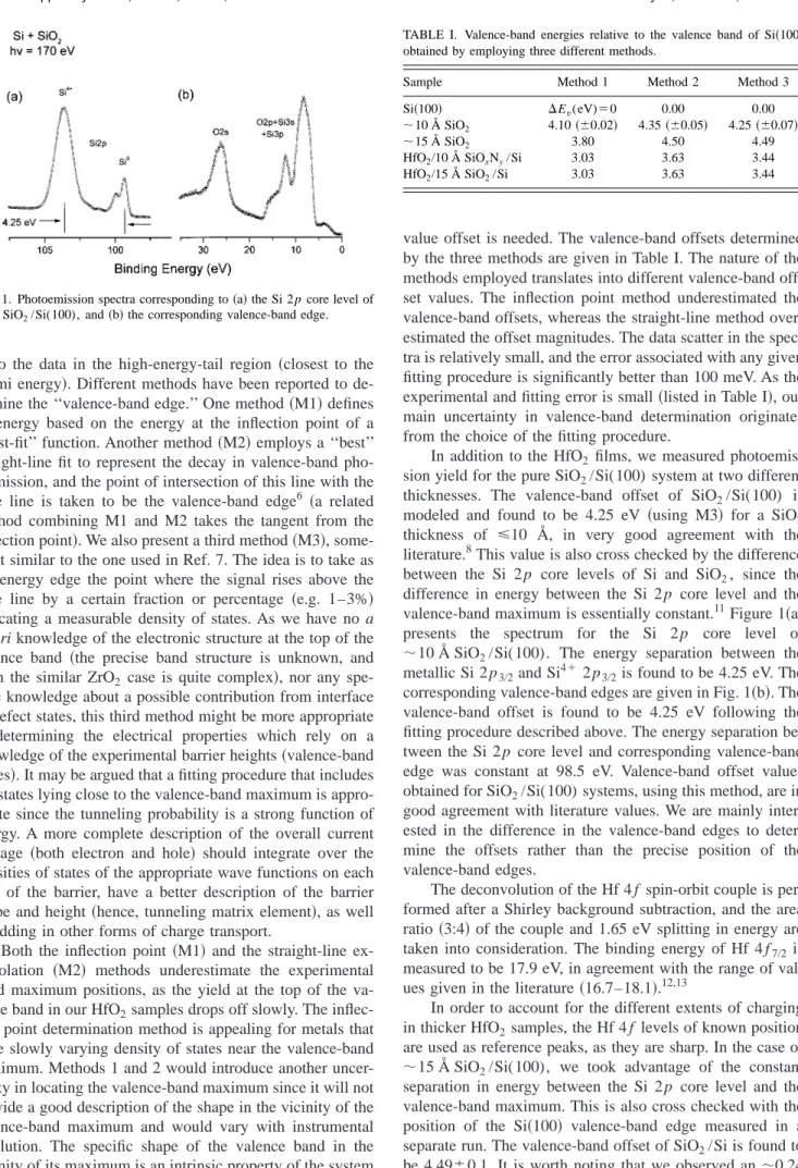
thickness of ⭐10 Å, in very good agreement with the literature.8This value is also cross checked by the difference between the Si 2 p core levels of Si and SiO2, since the difference in energy between the Si 2 p core level and the valence-band maximum is essentially constant.11Figure 1共a兲 presents the spectrum for the Si 2 p core level of
⬃10 Å SiO2/Si(100). The energy separation between the
metallic Si 2 p3/2and Si4⫹ 2 p3/2is found to be 4.25 eV. The
corresponding valence-band edges are given in Fig. 1共b兲. The valence-band offset is found to be 4.25 eV following the fitting procedure described above. The energy separation be-tween the Si 2 p core level and corresponding valence-band edge was constant at 98.5 eV. Valence-band offset values obtained for SiO2/Si(100) systems, using this method, are in
good agreement with literature values. We are mainly inter-ested in the difference in the valence-band edges to deter-mine the offsets rather than the precise position of the valence-band edges.
The deconvolution of the Hf 4 f spin-orbit couple is per-formed after a Shirley background subtraction, and the area ratio 共3:4兲 of the couple and 1.65 eV splitting in energy are taken into consideration. The binding energy of Hf 4 f7/2 is measured to be 17.9 eV, in agreement with the range of val-ues given in the literature 共16.7–18.1兲.12,13
In order to account for the different extents of charging in thicker HfO2 samples, the Hf 4 f levels of known position
are used as reference peaks, as they are sharp. In the case of
⬃15 Å SiO2/Si(100), we took advantage of the constant
separation in energy between the Si 2 p core level and the valence-band maximum. This is also cross checked with the position of the Si共100兲 valence-band edge measured in a separate run. The valence-band offset of SiO2/Si is found to
be 4.49⫾0.1. It is worth noting that we observed an ⬃0.24 eV increase in the valence-band maximum in the oxide for thicknesses of ⬃10 and ⬃15 Å, as in Ref. 8. In a separate
FIG. 1. Photoemission spectra corresponding to共a兲 the Si 2p core level of 10 Å SiO2/Si(100), and共b兲 the corresponding valence-band edge.
TABLE I. Valence-band energies relative to the valence band of Si共100兲 obtained by employing three different methods.
Sample Method 1 Method 2 Method 3
Si共100兲 ⌬Ev(eV)⫽0 0.00 0.00
⬃10 Å SiO2 4.10共⫾0.02兲 4.35共⫾0.05兲 4.25共⫾0.07兲
⬃15 Å SiO2 3.80 4.50 4.49
HfO2/10 Å SiOxNy/Si 3.03 3.63 3.44
HfO2/15 Å SiO2/Si 3.03 3.63 3.44
paper we will discuss energy referencing 共to vacuum and Fermi levels兲, charging, initial state and final state effects, and band bending, all of which make energy-level determi-nation complex.
It is important to note that the valence band of the HfO2/SiO2/Si system 共Fig. 2兲 presents an offset of ⫺1.05 ⫾0.1 eV with respect to that of SiO2/Si. Therefore, it can be
inferred that the valence-band edge of HfO2 lies within ⫺1.05 eV of the valence-band edge of silicon dioxide.
Re-cently, Robertson14 calculated the valence- and conduction-band offsets of various oxides on silicon. He reported valence-band-offset values of 4.4 and 3.4 eV for SiO2/Si and
HfO2/Si, respectively. Accordingly, a valence-band offset of
up to⫺1.0 eV can be expected for the HfO2/SiO2system, in
very good agreement with our findings.
The valence-band edges of HfO2/10 Å SiOxNy/Si and
HfO2/15 Å SiO2/Si were found to be at the same position 共Fig. 2兲. Hence, nitrogen incorporation in this oxynitride
does not seem to affect the valence-band position, at least within the level given by our experimental resolution and fitting procedure. The intensity differences in the valence-band region can be attributed to the difference in nitrogen incorporation in the bottom oxide.
The determined valence-band offsets for the systems studied here can be used to derive values for conduction-band offsets if the gap is known:
⌬Ec共HfO2⫺Si兲⫽Eg共HfO2兲⫹⌬Ev共SiO2⫺HfO2兲 ⫺⌬Ev共SiO2⫺Si兲⫺Eg共Si兲. 共1兲
We are cognizant that there is no consensus on the values to be used for the band gap of HfO2 共or even the most reliable
experimental method to determine the gap兲. If we choose a HfO2 band gap of 5.7 eV, as has been suggested by some,
1
then the conduction-band offset becomes ⬃1.2 eV (⫽5.7
⫹1.1⫺4.5⫺1.1 eV). Unfortunately, the uncertainty on this
number is high, primarily because of uncertainties in the band gap共numbers above 6 eV have been reported兲. Even if the HfO2– Si conduction-band offset is of order 1 eV,
tunnel-ing will be less than a simple calculation would lead one to believe, since there are usually 1–2 ML of SiO2 situated between the HfO2 and Si. On-going photoemission, inverse photoemission, and other studies of ultrathin HfO2and other high-⑀kfilms (EOT⬍20 Å) will help better understand these effects as well as determine band gaps and conduction-band offsets more accurately for these technologically critical ma-terial systems.
We have estimated the valence-band maximum of the systems under investigation using several different methods. The valence-band edges of HfO2/10 Å SiOxNy/Si and
HfO2/15 Å SiO2/Si were found to be at the same position
within experimental error, inferring that nitrogen doping of the bottom oxide does not significantly change the position of the valence-band maximum. The valence band of HfO2/SiO2/Si and HfO2/SiOxNy/Si systems present an
off-set of ⫺1.05⫾0.1 eV with respect to that of SiO2/Si.
The authors acknowledge the Semiconductor Research Corporation and the National Science Foundation for finan-cial support. The authors would like to thank M. Banasak-Holl, F. R. McFeely, Glen Wilk, Evgeni Gusev, Ed Cartier, Gerry Lucovsky, V. Misra, R. Opila, and Jack Rowe for their help in various parts of this work.
1G. D. Wilk, R. M. Wallace, and J. M. Anthony, J. Appl. Phys. 89, 5243
共2001兲.
2A. I. Kingon, J.-P. Maria, and S. K. Streiffer, Nature共London兲 406, 1032
共2000兲.
3K. Kukli, J. Aarik, A. Aidla, H. Siimon, M. Ritala, and M. Leskela, Appl.
Surf. Sci. 112, 236共1997兲.
4
C. T. Hsu, Y. K. Su, and M. Yokoyama, Jpn. J. Appl. Phys., Part 1 31, 2501共1992兲.
5B. H. Lee, L. Kang, R. Nieh, W.-J. Qi, and J. C. Lee, Appl. Phys. Lett. 76,
1926共2000兲.
6
S. Miyazaki, J. Vac. Sci. Technol. B 19, 2212共2001兲.
7J. W. Keister, J. E. Rowe, J. J. Kolodziej, H. Niimi, T. E. Madey, and G.
Lucovsky, J. Vac. Sci. Technol. B 17, 1831共1999兲.
8Hattori, in Fundamental Aspects of Ultrathin Dielectrics on Si-based
De-vices, edited by E. Garfunkel, E. P. Gusev, and A. Y. Vul’共Kluwer
Aca-demic, Dordrecht, The Netherlands, 1998兲, pp. 241–256.
9E. A. Kraut, R. W. Grant, J. R. Waldrop, and S. P. Kowalczyk, Phys. Rev.
B 28, 1965共1983兲.
10S. Sayan, S. Aravamudhan, B. W. Busch, H. W. Schulte, F. Cosandey, G.
D. Wilk, T. Gustafson, and E. Garfunkel, J. Vac. Sci. Technol. A 20, 507
共2002兲.
11F. J. Himpsel, F. R. McFeely, A. Taleb-Ibrahimi, J. A. Yarmoff, and G.
Hollinger, Phys. Rev. B 38, 6084共1988兲.
12D. D. Sarma and C. N. R. Rao, J. Electron Spectrosc. Relat. Phenom. 20,
25共1980兲.
13C. Morant, L. Galan, and J. M. Sanz, Surf. Interface Anal. 16, 304共1990兲. 14J. Robertson, J. Vac. Sci. Technol. B 18, 1785共2000兲.
FIG. 2. Photoemission spectra of SiO2/Si共a兲, HfO2/10 Å SiOxNy/Si共b兲,
and HfO2/15 Å SiO2/Si. 共c兲 systems. The right-hand panel of the figure displays our fitting procedure. In the upper-right hand, the inset shows an example of the difference of the photoemission yield at the top of the valence-band region.共The energy axis of one spectrum has been shifted, approximately 1 eV, to demonstrate the difference in shape in the vicinity of valence-band maximum.兲
2137