PHYSICS OF NONRADIATIVE ENERGY
TRANSFER IN THE COMPLEX MEDIA OF
0D, 2D AND 3D MATERIALS
a dissertation submitted to
the graduate school of engineering and science
of bilkent university
in partial fulfillment of the requirements for
the degree of
doctor of philosophy
in
physics
By
Aydan Yeltik
July 2016
PHYSICS OF NONRADIATIVE ENERGY TRANSFER IN THE COMPLEX MEDIA OF 0D, 2D AND 3D MATERIALS
By Aydan Yeltik July 2016
We certify that we have read this dissertation and that in our opinion it is fully adequate, in scope and in quality, as a dissertation for the degree of Doctor of Philosophy.
Hilmi Volkan Demir(Advisor)
Bilal Tanatar
D¨on¨u¸s Tuncel
Bekir Sıtkı Kandemir
Adil Denizli
Approved for the Graduate School of Engineering and Science:
Levent Onural
Director of the Graduate School ii
ABSTRACT
PHYSICS OF NONRADIATIVE ENERGY TRANSFER
IN THE COMPLEX MEDIA OF 0D, 2D AND 3D
MATERIALS
Aydan Yeltik Ph.D. in Physics Advisor: Hilmi Volkan Demir
July 2016
Quantum-confined colloidal nanostructures with strong excitonic properties have emerged as promising light harvesting components in photonics and optoelec-tronics over the past 20 years. With their favorable photophysical character-istics, three-dimensional-confined colloidal quantum dots and 2D-confined col-loidal quantum wells have garnered great attention in the fields ranging from biology and chemistry to physics and engineering. It is technologically signifi-cant to utilize the key characteristics of these brightly luminescent nanomaterials through hybridizing and/or interfacing with various technological materials in-cluding 3D bulk silicon, graphene based 2D structures such as graphene oxide and reduced graphene oxide, and 2D layered transition metal dichalcogenides such as molybdenum disulphide. Compelling partnership of these appealing ma-terials can be achieved through the nonradiative energy transfer (NRET), which is a phenomenon involving both the exciton and charge transfer mechanisms. Along with the hybrids of low dimensional particles with the conventional bulk materials, the closely interacting structures of these colloidal and layered nanoma-terials have widespread interest at both the fundamental science and application levels. From these physical and technological points of view, in this thesis, we ad-dressed important scientific problems and proposed innovative solutions including both the experimental and theoretical approaches in interfacing complex media of 0D, 2D and 3D materials and showing strong NRET interactions. Our key achievements include high excitonic enhancement in silicon and graphene based materials with the integration of nanoparticles, comprehensive photophysical in-vestigation of the newly emerging nanomaterials and successful tailoring of the colloidal nanostructures to the next-generation optoelectronic applications. Keywords: Nonradiative energy transfer, colloidal quantum dots, colloidal quan-tum wells, layered quanquan-tum wells, semiconductors, excitonics, charge transfer, light harvesting.
¨
OZET
0, 2 VE 3 BOYUTLU MALZEMELER˙IN
OLUS
¸TURDU ˘
GU KARMAS
¸IK YAPILARDA IS
¸INIMSIZ
ENERJ˙I TRANSFER˙IN˙IN F˙IZ˙I ˘
G˙I
Aydan Yeltik Fizik, Doktora
Tez Danı¸smanı: Hilmi Volkan Demir Temmuz 2016
Son yıllarda, g¨u¸cl¨u eksitonik ¨ozelliklere sahip kuvantum sınırlı koloidal nanoyapılar fotonik ve optoelektronik alanlarında yaygın bir kullanıma ula¸smı¸stır. 3 boyutta sınırlı koloidal kuvantum noktaları ve 2 boyutta sınırlı koloidal kuvantum kuyuları ¨ust¨un fotofiziksel ¨ozellikleri ile biyoloji ve kimyadan fizik ve m¨uhendisli˘ge kadar bir¸cok alanda b¨uy¨uk ilgi uyandırmı¸stır. Bu ı¸sık sa¸can nanomalzemeler ile 3 boyutlu silikon, 2 boyutlu grafen ve 2 boyutlu dikalkogenitler gibi teknolojik a¸cıdan ¨onemli malzemelerin melez ve/veya arabirim yapıları ¨ozellikle ¨onem arz etmektedir. Bu yapılarda eksitonik ve eksitonik olmayan transfer mekanizmalarını i¸ceren ı¸sınımsız enerji transferi ger¸cekle¸sebilmektedir. Farklı kuvantum sınırlı malzemelere sahip bu yapılara hem temel bilim hem de teknolojik uygulama seviyesinde yaygın bir ilgi mevcuttur. Bu tezde, deneysel ve teorik yakla¸sımlar kullanarak 0, 2 ve 3 boyutlu malzemelerin karma¸sık yapılarının olu¸sturulması ve ortaya ¸cıkan g¨u¸cl¨u ı¸sınımsız enerji transferi etkile¸simlerinin incelenmesi konularındaki ¨onemli bilimsel problemleri ve ¨onerdi˘gimiz yenilik¸ci ¸c¨oz¨umleri sunmaktayız. Bu tezin i¸cerdi˘gi ¨onemli ba¸sarılarımız arasında silikon ve grafen tabanlı yapılarda kuvantum sınırlı koloidal par¸cacıklar kullanarak eksitonik verimlilik artı¸sı, yeni ortaya ¸cıkan nanomalzemelerin fotofiziksel a¸cıdan kapsamlı ¸sekilde incelenmesi ve yeni nesil optoelektronik uygulamalarda koloidal nanopar¸cacıkların ba¸sarılı kullanımı bulunmaktadır.
Anahtar s¨ozc¨ukler: I¸sınımsız enerji transferi, koloidal kuvantum noktacıklar, koloidal kuvantum kuyuları, katmanlı kuvantum kuyuları , yarı iletkenler, eksiton, y¨uk transferi, ı¸sık hasadı.
Acknowledgement
First of all, I would like to take this opportunity to express my gratitude to my supervisor Prof. Hilmi Volkan Demir, whose support, motivation and guidance made this thesis work along with other great things possible.
I would like to thank my committee members Prof. Bilal Tanatar, Prof. D¨on¨u¸s Tuncel, Prof. Bekir Sıtkı Kandemir and Prof. Adil Denizli for accepting to be in my thesis jury and for their support.
I would like to thank all the past and present members of Demir Group for their friendship and having great fun together. I would also like to thank all my other friends at Bilkent University. And, I would like to acknowledge the instructors, engineers and graduate students at UNAM.
Finally, I would like to thank my family for their love, support and encourage-ment without any expectation.
vi
Contents
Chapter 1 1
Introduction 1
1.1 Structure of the thesis 2
Chapter 2 5
Background on Materials, Methods and Physical Phenomena 5
2.1 Materials 5
2.1.1 Colloidal 0D semiconductor nanocrystals: colloidal quantum dots 5 2.1.2 Colloidal quasi-2D semiconductor nanocrystals: nanoplatelets 13 2.1.3 Layered 2D nanomaterials: graphene, graphene oxide, reduced
graphene oxide and MoS2 19
2.1.4 Indirect bandgap 3D semicondutor materials: silicon 23
2.2 Methods 25
2.2.1 Steady-state and time-resolved fluorescence spectroscopy 25 2.2.2 Measuring the optical absorption properties of nanoemitters 30 2.2.3 Fabrication and characterization of hybrid structures 31
2.2.4 Growth of layered 2D MoS2 nanomaterials 32
2.3 Physical phenomena 34
2.3.1 Excitonic nonradiative energy transfer mechanism 34 2.3.2 Nonexcitonic nonradiative energy transfer mechanism 43
vii
Excitonic Nonradiative Energy Transfer by Using Colloidal 0D Semiconductor
Nanocrystals 47
3.1 Phonon-assisted excitonic nonradiative energy transfer into silicon by using
quantum dot nanoemitters 50
3.1.1 Motivation 50
3.1.2 Experiment and theory 52
3.1.3 Results and discussion 75
3.1.4 Summary 86
3.2 Enhancement of excitonic nonradiative energy transfer into bulk silicon with
the hybridization of cascaded quantum dots 87
3.2.1 Motivation 87
3.2.2 Experiment and theory 88
3.2.3 Results and discussion 99
3.2.4 Summary 105
3.3 Evidence for nonradiative energy transfer from quantum dots into
graphene-based nanomaterials and a short study including MoS2 106
3.3.1 Motivation 106
3.3.2 Experiment 108
3.3.3 Results and discussion 111
3.3.4 Summary 118
3.3.5 Additional study including MoS2 118
Chapter 4 123
Excitonic Nonradiative Energy Transfer by Using Colloidal quasi-2D Semiconductor
Nanocrystals 123
4.1 Experimental determination of the absorption cross-section and molar
extinction coefficient of colloidal nanoplatelets 126
4.1.1 Motivation 126
4.1.2 Experiment 128
4.1.3 Results and discussion 131
viii
4.2 Nonradiative energy transfer between quasi-2D colloidal doped and undoped
semiconductors 146
4.2.1 Motivation 146
4.2.2 Experiment 148
4.2.3 Results and discussion 149
4.2.4 Summary 160 Chapter 5 161 Conclusions 161 5.1 Concluding remarks 161 5.2 Future outlook 164 5.3 Contributions 165 Bibliography 167
ix
List of Figures
Figure 2.1. (a) A TEM image, (b) an illustration together with (c) the energy-band diagram of a semiconductor nanocrystal (e.g. a CQD) (a rough representation). ... 7 Figure 2.2. (a) Photograph of PL from CdSe/ZnS QDs of increasing size (left to right) illuminated under UV light. (b) Qualitative changes in the QD bandgap energies, Eg, and density of states for CdSe QD510 (2.7nm diameter), QD530 (2.9 nm), QD555 (3.5 nm), QD570 (3.8 nm), QD590 (4.3 nm), and QD610 (4.8 nm). The conduction (CB) and valence (VB) bands of bulk CdSe are shown for comparison and the energy scale is expanded as 10E for clarity. Transitions for absorption and band edge emission are also presented. (Adapted and reprinted with permission from Ref. [7]. Copyright 2011, American Chemical Society.) ... 9 Figure 2.3. Typical absorbance and emission spectra of CQDs. ... 10 Figure 2.4. Schematic representation of a zincblende 4 monolayer (ML) CdSe NPL. . 14 Figure 2.5. TEM images of (a) 4ML and (b) 5ML NPLs with both the small and large lateral sizes, and their corresponding thicknesses. ... 15 Figure 2.6. UV-Vis absorbance and PL emission spectra of 4ML CdSe NPLs. ... 17 Figure 2.7. Energy diagrams of an optical emitter and a nearby graphene monolayer film along with schematic representation of the sample structure. (Reprinted with permission from Ref. [124]. Copyright 2013, American Chemical Society.) ... 21 Figure 2.8. Band structure of bulk silicon. (Reprinted with permission from Ref. [149]. Copyright 2001, Oxford University Press.) ... 24 Figure 2.9. Logic for operation of the TRF system. ... 27
x
Figure 2.10. FluoTime 200 TRF system. ... 28 Figure 2.11. Schematic representation of a TRF system. ... 28 Figure 2.12. CVD growth system that we use in Demir laboratory. ... 33 Figure 2.13. (a) Exemplary SEM images, (b) Raman spectrum and (c) PL spectrum of MoS2 single layer structures. ... 33
Figure 2.14. (a) Simplified Jablonski diagram including excitation and relaxation transitions, followed by radiative decay (kR), nonradiative decay (kNR) or FRET (kFRET).
After the FRET, the acceptor is in an excited state (A*), followed by radiative or nonradiative decay to the ground state (A). (b) Different energy pathways after donor excitation (hνex) possibly leading to luminescence emission of D (hνD) or A (hνA).
(Reprinted with permission from Ref. [159]. Copyrigt 2014, Wily-VH.) ... 36 Figure 2.15. The overlaping area of the area-normalized emission spectrum of Donor and the extinction coefficient spectrum of Acceptor, defining the overlap integral J. . 39 Figure 2.16. FRET efficiency (ηFRET) as a function of donor-acceptor separation distance (r). ... 40
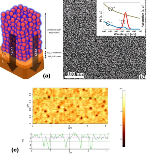
Figure 3.1. (a) Schematic of the hybrid nanostructure of multi-monolayer CQDs and silicon separated by controlled Al2O3 separation thickness. Here l = 1.65 nm is the
native SiO2 film thickness, h is the distance between the top-most oxide layer and
center of the first CQD layer, X ranging from 0.0 to 4.0 nm is the Al2O3 film thickness,
and d is the distance from a CQD monolayer center of interest to the bulk silicon surface. The CQDs of the same monolayer are assumed to have the same exciton transfer contribution to bulk silicon. (b) SEM image of the CQDs furnished on the Al2O3/SiO2/Si structures. Inset shows optical absorption and PL spectra of the CQDs
(black and green curves, respectively) and absorption spectrum of silicon (red curve). (c) Atomic force microscopy image of the 10-monolayer-equivalent CQD film on top of silicon with the height profile of the line shown inside the AFM image. ... 54 Figure 3.2. Experimental fluorescence decays of 10-monolayer–equivalent CQD film on silicon substrate with 0.0, 1.0, 2.0 and 4.0 nm of Al2O3 separation layer and on
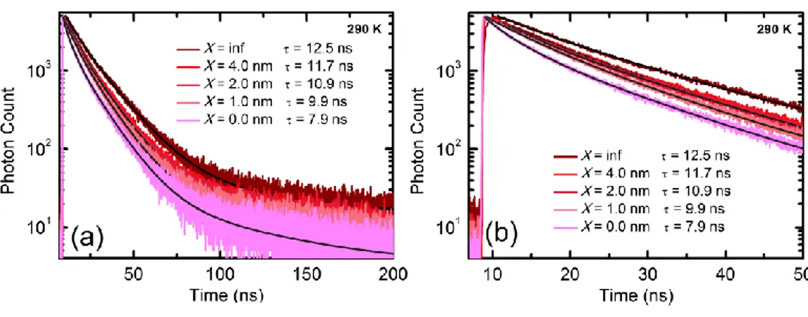
sapphire as reference sample: (a) over a time decay of 200 ns and (b) zooming in the first 50 ns. The multi-exponential fits are shown inside the decay curves with the averaged lifetimes reported at the bottom. ... 56
xi
Figure 3.3. Temperature dependence of PL intensity of the CQDs coated on the Al2O3/SiO2/Si and sapphire substrates. ... 57
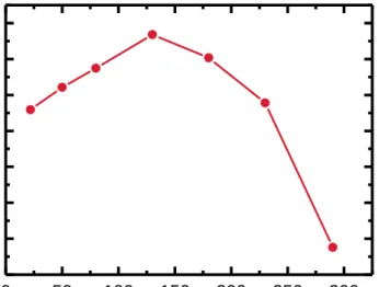
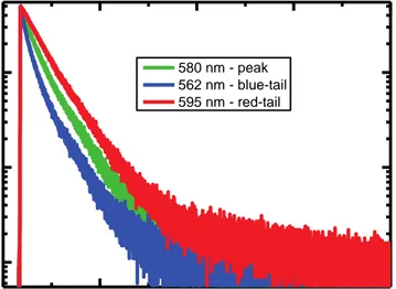
Figure 3.4. Fluorescence decays of the ten-monolayer-equivalent CQDs measured at three different spectral positions (peak, blue- and red-tail) at FWHM. ... 59 Figure 3.5. TRF decays of 10-monolayer-equivalent CQD film over silicon substrate with 0.0, 1.0, 2.0 and 4.0 nm thick Al2O3 separation layer and over sapphire, which
were recorded at 22 K. ... 60 Figure 3.6. A schematic of the studied 0D 3D hybrid structure. Here, z is the dielectric thickness of the effective oxide layer on silicon, h is the distance between the dipole and the topmost dielectric layer, l = 1.65 nm is the SiO2 film thickness, X
ranging from 0 to 4.0 nm is the Al2O3 film thickness and d is the distance from a QD
monolayer center of interest to the bulk silicon. ... 63 Figure 3.7. Temperature dependence of fluorescence lifetime of the CQDs integrated on top of (a) 0.0 nm, (b) 1.0 nm, (c) 2.0 nm and (d) 4.0 nm thick Al2O3 layer on
SiO2/Si. Black squares are amplitude averaged experiment lifetimes. Green diamonds
are the lifetimes of the CQDs on sapphire as the reference sample corrected for the refractive index difference with silicon. Red circles are the calculated lifetimes of the CQDs using the “temperature-independent” energy transfer model. Blue up-triangles are the calculated lifetimes of the CQDs using the energy transfer model which considers the temperature-dependent complex dielectric function of silicon, thus “phonon-assisted” model. Orange down-triangles are the calculated lifetimes of the CQDs using the “phonon-assisted” energy transfer model with the additional inclusion of the temperature-dependent QY of the donor CQDs; thus, it is called “full temperature-dependent” model. ... 76 Figure 3.8. (a) Energy diagram illustrating the exciton transfer from the donor CQD to the acceptor silicon due to the Coulomb interaction between the donor-acceptor pair. The phonon-assisted process is shown as the lateral arrows to make up for the momentum mismatch in silicon. (b) Some of the Feynman diagrams for the phonon-assisted processes important for transfer of energy from a CQD to an indirect-band semiconductor. These diagrams include phonon-emission processes in the conduction band. ... 79
xii
Figure 3.9. Experimental FRET rates as a function of temperature. Orange squares correspond to the FRET without Al2O3. Red circles correspond to the FRET for 1.0 nm
Al2O3 thickness. Blue up-triangles correspond to the FRET for 2.0 nm Al2O3 thickness.
Green down-triangles correspond to the FRET for 4.0 nm Al2O3 thickness. The FRET
rates in this graph were obtained taking the modified reference rates into account. .... 83 Figure 3.10. Energy transfer rates as a function of the temperature for each case: Al2O3
thickness of 0.0, 1.0, 2.0 and 4.0 nm. Black squares correspond to the experimental data. Red circles represent the FRET without phonon assistance, blue up-triangles include phonon assistance, orange down-triangles both consider the phonon assistance and temperature dependent QY change of the CQDs. ... 84 Figure 3.11. FRET efficiency as a function of the temperature in the range of ... 85 Figure 3.12. (a) Schematic for the gradient energy transfer from the cascaded GQD/RQD bilayer into bulk Si. (b) Emission and absorption spectra of CdTe GQDs and CdTe RQDs (green and red curves, respectively), and absorption spectrum of bulk Si (blue curve). ... 90 Figure 3.13. Energy diagram for the excitation transfer from a bilayer of red (green)-emitting CQDs to bulk Si. Horizontal arrows represent the interaction energy between the energy levels. Vertical arrow shows relaxation process between the excited levels. Dash vertical arrows depict the relaxation between the lowest excited state and ground state. ... 93 Figure 3.14. Energy diagram for the excitation transfer from a layer of green-emitting CQDs and a layer of red-emitting CQDs to bulk Si. Horizontal arrows represent the interaction energy between the energy levels. Vertical arrows show relaxation process between the excited levels. Dash vertical arrows depict the relaxation between the lowest excited state and ground state. ... 95 Figure 3.15. Exciton population (in %) for the cases of: (1) QDG QDR Si (black curve); (2) QDR QDR Si (red curve); and (3) QDG QDG Si (green
curve). ... 97 Figure 3.16. Excitonic quenching factor (left) and enhancement factor (right) as a function of time for the relative case 1. ... 98 Figure 3.17. Excitonic quenching factor (left) and enhancement factor (right) as a function of time for the relative case 2. ... 99
xiii
Figure 3.18. Excitonic quenching factor (left) and enhancement factor (right) as a function of time for the relative case 3. ... 99 Figure 3.19. TRF spectroscopy at 535 nm from the bilayer integration of GQDs on Si (dark green solid line), GQD/RQD on Si (dark orange solid line), GQDs on quartz (green solid line), GQD/RQD on quartz (orange solid line), and the laser diode response function (navy solid line). ... 100 Figure 3.20. TRF spectroscopy at 640 nm from bilayer integration of RQDs on Si (wine solid line), GQD/RQD on Si (magenta solid line), RQDs on quartz (red solid line), GQD/RQD on quartz (pink solid line), and the laser diode response function (navy solid line). ... 102 Figure 3.21. (a) Exciton population for the cases of: (1) GQD RQD Si (black solid line); (2) RQD RQD Si (red solid line); and (3) GQD GQD Si
(green solid line). (b) Excitonic quenching factor (left) and enhancement factor (right) as a function of time for Case 1 with respect to Case 2. ... 105 Figure 3.22. (a) Schematic representation of the hybrid CQD/HfO2/GO structure. (b)
Energy diagram for the FRET from CQD into GO based acceptor. ... 109 Figure 3.23. Tapping-mode AFM image of 5 nm HfO2 layer coated on GO film on
quartz together with the height profile. ... 110 Figure 3.24. (a) Tapping mode AFM image of the GO thin film on quartz. (b) Height profile along the red line presented in (a). Inset shows the AFM image of an isolated single GO sheet on quartz. (c) Raman spectra of GO and RGO thin film reduced at 900 °C. (d) XPS spectra of GO and RGO thin films reduced at 625 and 900 °C. (e) Normalized absorption (black line) and PL (red line) spectra of CdSe/CdS CQDs with normalized absorption of GO solution (blue line). (f) HR-TEM image of the CQDs used in the study. ... 112 Figure 3.25. (a) Experimental TRF decays of the CQDs on GO and RGO thin films on quartz for the HfO2 separation distances of 4.0 nm and 0.2 nm; and 20.0 nm for the CQDs without GO and RGO at the bottom (Reference). Solid black lines are multi-exponential fits to the data, and gray decay curve is the laser diode response function (IRF). (b) TRF lifetimes of the CQDs as a function of the distance from GO and RGO; and of the reference. (c) Separation distance dependence of the NRET rates of the CQDs on GO and RGO reduced at 900 °C. Inset shows the experimental decays of the
xiv
CQDs on GO, RGO reduced at 625 °C, RGO reduced at 900 °C and the theoretical decay of the CQDs on graphene (d) NRET efficiency of the CQDs on GO and RGO reduced at 900 °C as a function of the separation distance. ... 117 Figure 3.26. SEM images of MoS2 layers growth via CVD. ... 119
Figure 3.27. PL and Raman spectra of MoS2 layers growth via CVD. ... 120
Figure 3.28. Microscope images of MoS2 layer growth around the rough surface points.
... 120 Figure 3.29. Layered 2D MoS2 structures growth on patterned silicon substrates to
examine the effect of surface roughness to the flow pattern and thus the growth layers. ... 121 Figure 3.30. TRF energy transfer rates and efficiencies of CQD-MoS2 hybrids
depending on the environmental temperature. ... 122
Figure 4.1 UV-Vis absorbance spectra, PL spectra and TEM images of the (a) 4 ML and (b) 5 ML thick CdSe NPLs having various lateral sizes. ... 132 Figure 4.2 Peak positions of the PL FWHM, PL, hh-e transition and lh-e transition of (a) 4 ML NPLs and (b) 5 ML NPLs for varying lateral sizes. ... 133 Figure 4.3 UV-Vis absorbance spectra of the reaction host medium solution containing cadmium acetate, oleic acid and octadecene, reaction mixture and final mixture after the extraction process of the NPLs. ... 134 Figure 4.4 Absorption cross-section spectra of 4 ML CdSe NPL samples with varying lateral sizes obtained by using the (a) Se and (b) Cd concentrations from ICP-OES measurements. Lateral size dependence of the absorption cross-section (c) at the energy of hh-e transition peak and (d) at high photon energy 3.1 eV. ... 137 Figure 4.5 Absorption cross-section spectra of 5 ML CdSe NPL samples with varying lateral sizes obtained by using the (a) Se and (b) Cd concentrations from ICP-OES measurements. Lateral size dependence of the absorption cross-section (c) at the energy of hh-e transition peak and (d) at high photon energy 3.1 eV. ... 139 Figure 4.6 Lateral size dependence of the extinction coefficients of (a) 4 ML CdSe NPLs and (b) 5 ML CdSe NPLs obtained by using the Se concentrations from ICP-OES measurements. ... 140
xv
Figure 4.7 Absorption cross-section spectra of 4 ML CdSe NPL samples with varying lateral sizes obtained by using the (a) Se and (b) Cd concentrations from ICP-MS measurements. Lateral size dependence of the absorption cross-section (c) at the energy of hh-e transition peak. ... 142 Figure 4.8 Absorption cross-section spectra of 5 ML CdSe NPL samples with varying lateral sizes obtained by using the (a) Se and (b) Cd concentrations from ICP-MS measurements. Lateral size dependence of the absorption cross-section (c) at the energy of hh-e transition peak. ... 143 Figure 4.9 Dependence of the intrinsic radiative lifetime of the hh-e transition and the oscillator strength on the lateral size of (a) 4 ML and (b) 5 ML thick CdSe NPLs using the results obtained from the Se concentrations of ICP-OES measurements. ... 145 Figure 4.10 TEM images of the (a) Cu-doped 3ML core NPLs and (b) undoped 4ML/5ML CdSe/CdS core/shell NPLs. (c) Schematic of our hybrid structure including the Cu-doped and undoped NPLs. (d) Photoluminescence and absorbance spectra of the Cu-doped and undoped NPLs in toluene. ... 149 Figure 4.11 Steady-state PL spectra of the solid films of donor (orange), only-acceptor (red) and donor–only-acceptor having D/A = 2.5x10⁻⁵ (green) cases. ... 150 Figure 4.12 Time-resolved PL decay curves at the donor trap emission peak wavelength, 620 nm, for various D/A concentration ratios. ... 151 Figure 4.13 Time-resolved PL decay curves at the acceptor second excitonic absorption peak wavelength (598 nm) for various D/A ratios. ... 152 Figure 4.14 Time-resolved PL decay curves at the donor band-edge emission peak wavelength (465 nm) for various D/A ratios. Note: The data in (a) were continued in (b). ... 153 Figure 4.15 Time-resolved PL decay curves at the acceptor trap emission peak wavelength (660 nm) for various D/A ratios. Note: The data in (a) were continued in (b). ... 154 Figure 4.16 NRET efficiency as a function of Donor/Acceptor (D/A) molar ratio. ... 157 Figure 4.17 NRET efficiency for a single D/A pair as a function of D/A molar ratio. ... 158 Figure 4.18 (a) PLE spectra of the doped donor NPLs (orange) and the undoped acceptor NPLs (red) measured at their Cu-related emission peak wavelength (620 nm)
xvi
and excitonic emission peak wavelength (660 nm), respectively. (b) Photoluminescence excitation spectra of the samples having different D/A ratio, measured at 660 nm and then normalized at the second excitonic (e-lh transition) peak wavelength (598 nm) of the acceptor. Inset figure shows the enhancement of PLE through the NRET in the hybrid donor–acceptor samples. ... 159
xvii
List of Tables
Table 2.1. Typical separation distance ranges and distance dependences of various transfer mechanisms...44
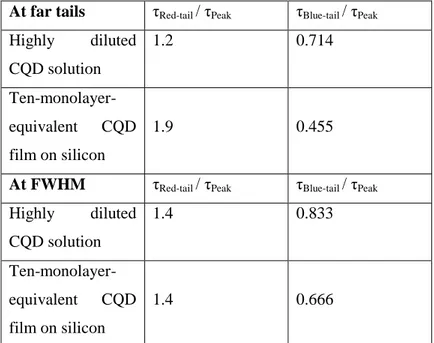
Table 3.1. Lifetime ratios of the CQDs in the emission spectra (lifetimes of the red-tail and blue-tail emission as compared to lifetime at the peak-emission wavelength) when measured for far tail-emission and at FWHM. ... 58 Table 3.2. Experimental QY and gamma ratios; and calculated radiative rate ratio for each temperature used in the study. ... 66 Table 3.3. Fluorescence lifetimes for the CQDs on quartz as the reference sample (corrected for refractive index variation) and on Si. ... 101
Table 4.1. Corresponding values of 4 ML and 5 ML thick CdSe NPLs at the energy of hh-e peak and at the high energy value 3.1 eV. ... 141 Table 4.2. PL decay lifetimes (τ), NRET rates and NRET efficiencies of the donor NPLs for the samples with varying D/A ratios. ... 156
1
Chapter 1
Introduction
Sustainable and renewable energy sources are envisaged to supply a significant portion of the energy demand increasing with the recent exponentially growing population in the world. Photonics technology has offered innovative and feasible optoelectronic solutions to this ultimately important energy consumption problem. Among the proposed solar-to-electric conversion systems, silicon-based photovoltaics and luminescent solar concentrators have been key elements in the modern world. As the optoelectronics of photovoltaic solar energy conversion is being developed, new photonic materials have been introduced to make low-cost, high-performance energy conversion systems. An important class of these materials consists of solution-processed, low-temperature grown nanocrystals as an alternative to high-temperature epitaxially grown semiconductors. These colloidal semiconductors exhibit superior properties including exciting optoelectronic properties, accompanied with low-cost synthesis and easy usage on arbitrary substrates. Therefore, utilization of the colloidal nanocrystals is expected to provide optical and electrical advantages for the next-generation solar light-harvesting systems. Today the most common type of the colloidal nanocrystals is the spherical ones, while are quasi zero-dimensional (0D) structures also known as colloidal quantum dots.
2
CQDs are promising nanomaterials also for the efficiency enhancement in newly emerging two-dimensional (2D)-material integrated optoelectronics. Atomically thin layers of 2D materials such as graphene and transition metal dichalcogenides have been studied in the recent years to be utilized in photonics technology. Their better carrier transporting and favorably larger exciton accepting properties are ultimately important together with the exotic characteristics of colloidal nanocrystals. Therefore, it is envisioned that the respective optical and electrical strengths of these materials will allow their efficient 0D-2D material hybrids to be used in novel nanotechnological devices in the future.
Recent years have witnessed many successful applications of the colloidal nanocrystals in photosensing technology. Their extraordinary properties including excitonic/multiexcitonic large absorption cross-section along with diverse band alignment and ease of utilization in device applications may open new routes for the high-sensitivity photosensors. In addition, very recent developments in the material engineering of colloidal semiconductor nanocrystals have provided new dimensionalities for the nanomaterials. One important outcome of these developments is the synthesis of colloidal quasi-2D flat semiconductor nanocrystals, which are also known as nanoplatelets (NPLs). These newly emerging rising stars with various superior properties, when compared to CQDs, exhibit great potential for the high-performance photosensing together with photovoltaic applications. Furthermore, ion doping provides additional useful characteristics to these quasi-2D structures and their quasi-0D counterparts, specifically for photovoltaics and luminescent solar concentrators. All in all, these doped and undoped quasi-0D and quasi-2D nanomaterials have great advantages to be used for opening up new directions for the future technological advances.
1.1 Structure of the thesis
In this thesis, we studied the physics of excitonic and nonexcitonic nonradiative energy transfer (NRET) mechanisms in the highly promising hybrids of 0D, 2D and 3D
3
materials. The thesis is organized in five chapters. In Chapter 2, we present a scientific background on the materials, methods and physical phenomena used in this thesis. We elaborate the materials section in three subsections listed as colloidal 0D semiconductor nanocrystals: colloidal quantum dots, colloidal quasi-2D semiconductor nanocrystals: nanoplatelets, layered 2D nanomaterials: graphene, graphene oxide, reduced graphene oxide and MoS2, indirect bandgap 3D semicondutor materials:
silicon. In the methods section, we explain how we utilized steady-state and time-resolved fluorescence spectroscopy, investigated the optical absorption properties of nanoemitters, fabricated and characterized the hybrid structures; and grew the layered 2D MoS2 nanomaterials. In the last section of this chapter, we explain the physical
phenomena of excitonic/nonexcitonic nonradiative energy transfer mechanisms. In Chapter 3, we present our studies on excitonic nonradiative energy transfer using colloidal 0D semiconductor nanocrystals. First, we elucidate phonon-assistance in the excitonic NRET from nanoemitters to an indirect bandgap 3D semiconductor. We further discuss the excitonic enhancement of NRET into bulk silicon by using the energy-gradient of cascaded nanoemitters. We strongly believe that the findings of these studies will be crucial in designing new silicon-based high-efficiency solar light-harvesting systems through the excitonic sensitization of silicon. The third section of this chapter includes the study of excitonic NRET from CQDs to graphene variants including graphene oxide and reduced graphene oxide. Furthermore, in a small section, we present the growth procedures of MoS2 layers and preliminary NRET study on the
hybrids of these 2D structures with CQDs.
In Chapter 4, we uncover the optical properties of newly emerging quasi-2D nanoplatelets. In the first section of this chapter, we present the experimental determination of the absorption cross-section and molar extinction coefficient of colloidal CdSe NPLs. In this way, we provide fundamental information for the investigation of excitonic NRET in the systems including colloidal quasi-2D semiconductor nanocrystals. In the second section, we present the study on NRET between quasi-2D colloidal doped and undoped semiconductors depending on donor/acceptor molar ratios in the solid hybrid films. It is envisioned that much further improvement is possible for the nanocrystal-based optoelectronics through the
4
integration of Cu-doped NPLs together with undoped NPLs to the current systems such as photovoltaics, luminescent solar concentrators, LEDs and displays.
In Chapter 5, we make the concluding remarks on this thesis, and present the future outlook and the contributions of the thesis to the literature.
5
Chapter 2
Background on Materials, Methods and
Physical Phenomena
2.1 Materials
2.1.1 Colloidal 0D semiconductor nanocrystals: colloidal
quantum dots
Colloidal luminescent 0D semiconductor nanocrystals, or colloidal quantum dots (CQDs), are one of the most interesting nanomaterials emerging more than 2 decades ago. These appealing quantum-confined structures have great potential for numerous applications ranging from photonics and optoelectronics to biotechnology and medicine [1]. Some of the advantages of high-quality CQDs can be listed as the size and conformation tunable emission having narrow and symmetric profile, high luminescent quantum yield (QY), spectrally broad absorption band, large one- and two-photon absorption cross-sections, large Stokes shift, and high resistance to photobleaching and chemical degradation [2]–[8]. LED, lasing, solar energy and
6
display technologies are some of the applications for CQDs to be used in the field of optoelectronics [9], [10]. Because of their unique electro-optical properties, they are also considered as favorable bioimaging and energy transferring labels [3]–[5], [11].
CQDs are 0D quantum systems having charge carriers that are confined in all three dimensions. Despite the epitaxial quantum dot, first coined by Reed et al. [12], [13], CQDs are solution-processed nanoparticles with crystalline or amorphous structure. High crystallinity of CQDs gives them high-quality optical and electronic properties. After the breakthrough exploratory works of Ekimov and Onushchenko in 1981 [14], Henglein in 1982 [15] and Efros and Efros in 1982 [16], the first colloidal form of quantum dots was reported in 1983 by Brus and coworkers at Bell Laboratories [17]. In contrast to top-down epitaxial approach, Brus et al. developed a new technique using bottom-up synthesis route [18]. After these first accounts, detailed photophysics and chemistry of CQDs has been also studied by Bawendi, Alivisatos, Guyot-Sionnest and many others [19]–[21]. Binary/ternary alloys of these 0D systems such as CdS, ZnS, CdSe, CdTe, InP, CdZnS, InGaAs, their core/shell forms such as CdSe/ZnS and CdSe/CdS, and various combinations of these structures have been synthesized generally by using wet chemistry techniques [22]–[28]. In addition to these well-established bottom-up synthesis methods, newly proposed and greener biotemplated approaches have started to be used recently among the CQD community despite their low quality products for now [29], [30].
CQDs are faceted nanoparticles owing to their crystalline nature and thus are roughly spherical in shape. They have sizes typically in the range of 1-10 nm in diameter [31]–[35] having 102 – 104 atoms in their crystalline structure (generally wurtzite or zinc-blende crystal structure). An illustration and a transmission electron microscopy (TEM) image together with energy-band diagram of a CQD are shown in Figure 2.1. Size and relative composition determine the optical properties of ternary CQDs while only size can affect these properties of binary CQDs. Size also specifies the surface-to-volume ratio of a CQD, which is an important parameter for the bioapplications of these nanostructures.
7
5 nm
(a)
(b)
(c)
Conduction Band Valence Band Bulk Semiconductor Semiconductor NanocrystalE
Figure 2.1. (a) A TEM image, (b) an illustration together with (c) the energy-band diagram of a semiconductor nanocrystal (e.g. a CQD) (a rough representation).
8
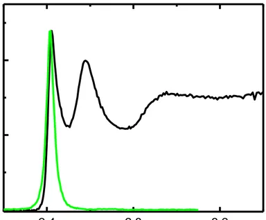
In bulk materials, energy levels atwhich electrons and holes occupy are quasi-continuum, forming the conduction band and the valence band as the lowest unoccupied and highest occupied energy levels of the system, respectively. However, CQDs have discrete energy levels of electron and hole because of the size and thus quantum confinement. Crystalline solids of CQDs are built up from their constituent atoms. When the number of atoms is high as in the bulk, linear combination of atomic orbitals constitutes the bands with a large density of states (DOS). The number of states is mediated by the number of atoms, therefore, since there is much smaller number of atoms in the CQDs, quantum confinement effects appear leading to the decrease in the number of DOS and thus the increase in the separations of energy levels. Size-tunable CQD PL, which is originated from this quantum confinement phenomenon, is shown in Figure 2.2. Typical UV-Vis absorbance and photoluminescence (PL) emission spectra of semiconductor CQDs are also represented in Figure 2.3.
9
Figure 2.2. (a) Photograph of PL from CdSe/ZnS QDs of increasing size (left to right) illuminated under UV light. (b) Qualitative changes in the QD bandgap energies, Eg, and density of states for CdSe QD510 (2.7nm diameter), QD530 (2.9 nm), QD555 (3.5 nm), QD570 (3.8 nm), QD590 (4.3 nm), and QD610 (4.8 nm). The conduction (CB) and valence (VB) bands of bulk CdSe are shown for comparison and the energy scale is expanded as 10E for clarity. Transitions for absorption and band edge emission are also presented. (Adapted and reprinted with permission from Ref. [7]. Copyright 2011, American Chemical Society.)
10 450 500 550 600 650
P
L
In
te
n
s
ity
A
b
s
o
rb
a
n
c
e
Wavelength (nm)
Figure 2.3. Typical absorbance and emission spectra of CQDs.
As the 3D version of particle-in-a-box character of CQDs, particle-in-a-sphere model is indicating that the allowed wave functions with the necessity of nodes at the surface of the CQD are determined by the nanocrystal dimensions [36]. From this model, the CQD bandgap energy is scaling as a 2, where a is the radius of the CQD [37]. However, Brus and coworkers recognized that the energy gap is also dependent on increasing electrostatic attraction leading to the shifting of PL spectrum to lower energies and on increasing kinetic energies related to confinement of the charges leading to the shifting of spectrum to higher energies. Brus obtained a general equation for the energy gap of CQDs by utilizing particle-in-a-sphere wave functions, effective mass approximation for the kinetic energy and hydrogenic Hamiltonian [21], [38]– [41]. The resultant formula is shown in Eq. 2.1, where EB is the bulk bandgap energy,
is the reduced mass for electron–hole pair, is the semiconductor dielectric constant, and ERy is the Rydberg energy for electron–hole pair.
11 2 2 2 2
( )
1.786
0.248
2
CQD B Rye
E
a
E
E
a
a
(2.1) 1 2 3 4Term 2 of Eq. (2.1) is defined as the energy of a particle-in-a-sphere and Term 3 is the energy between the electron and hole inside CQD through Coulombic interaction. Due to the large dielectric constants of semiconductors and thus significant screening, the bound electron-hole pair, also named as exciton, should have an additional tendency to keep itself near the CQD center to overcome dielectric screening and maximize Coulombic interaction. This fact is considered with the inclusion of Term 4 into the Eq. 2.1.
Quantum confinement has also a significant impact on the oscillator strength as well as that on the energy levels of the CQDs. There are two important physical phenomena directly related to the effect of quantum confinement on the probability of optical transition to an electronic state: Fermi’s Golden Rule and Heisenberg’s Uncertainty Principle. Fermi’s Golden Rule indicates that the oscillator strength of a transition is dependent on the matrix element associated with the mixture of the initial and final states and on the extent of overlap of these states. Energy states related to the optical absorption of semiconductors are mainly the electron and hole states. Therefore, following the Fermi’s Golden Rule, an increase in the overlap of electron and hole wavefunctions due to the quantum confinement leads to an enhancement in the oscillator strength. This is one reason for the sharp peaks in the absorption spectra of CQDs compared to the smoother spectra of the corresponding bulk materials [17], [38], [41], [42]. Second reason for these strong absorption peaks is Heisenberg’s Uncertainty Principle. The principle rules out that, owing to the quantum confinement, the position and energy of an electron in a CQD are well defined but the momentum is uncertain. Discrete states in the quantum-confined structure can be thought as a superposition of continuum states from the bulk crystal. Energy and momentum are conserved quantities in an optical transition; therefore uncertainty in the energy
12
enhances the probability that a given transition will satisfy these conditions. For this reason, closely spaced transitions in the bulk are compressed into a single and intense transition in a CQD [32], [42].
Energy levels in the CQDs are also mediated by the semiconductor material as well as the size at the nanometer scale. Optical excitation of the nanoparticle creates bound electron-hole pairs in a small volume compared to the exciton Bohr radius of the material. PL shift of the CQD over the wavelength range has an upper limit determined by this preferred distance between the electron and hole in its bulk material [43], [44]. On the other hand, the lowest limit in the PL shift is determined by the capability of high-quality synthesis of the CQD and the decreasing optical absorption [45]. Typical CQDs with high optical quality have full width at half maximum (FWHM) in the range of 25 - 30 nm and stead-state PL QY as high as 95% [5], [33], [46]. Time resolved fluorescence (TRF) lifetimes of CQDs depend on various parameters such as the quality, coating and environment but, for a typical CQD, TRF lifetime generally exceeds 10 ns exhibiting multi-exponential decay components [47], [48]. Absorption profile of the CQDs shows a broader wavelength spectrum extending to the UV and having increasing amount of intensity with the decrease in wavelength.
To date, CQDs have been involved into Förster resonance energy transfer (FRET) mechanisms as both exciton donor and exciton acceptor. In the studies utilizing CQDs as exciton donor, a wide range of exciton accepting nanomaterials including colloidal quantum wells, metallic nanoparticles, polymers, fluorescent dyes and fluorescent proteins have been used [49]. CQDs are generally favorable exciton donors due to several reasons such as the easy application of CQD-FRET results to Förster theory, ability to minimize emission cross-talk of donor and acceptor particles and ability to maximize the overlap integral in the Förster theory. CQDs are also adept acceptors for efficient FRET when they are coupled with the appropriate donors [7], [50] because of their superior properties such as large extinction coefficient and spectral overlap integral. Besides these hetero-FRET systems, which involve particles with distinct chemical conformations, CQDs have also been studied for homo-FRET investigation, which is the FRET among the same kind of species. With several favorable characteristics of CQDs in the aforementioned context, the concept of QD-FRET as a
13
fundamental spectroscopy technique may offer new, pragmatic and exciting approaches for applications in physics, chemistry, biology and engineering.
2.1.2 Colloidal quasi-2D semiconductor nanocrystals:
nanoplatelets
Colloidal luminescent quasi-2D semiconductor nanocrystals, which are commonly known as colloidal nanoplatelets (NPLs) or colloidal quantum wells, have been one of the key elements for modern nanotechnological applications since the first account of free-standing ultrathin semiconductor layers by Kotov and coworkers in 2006 [51].
Following the first attempts on the synthesis of cadmium-based colloidal NPLs by Kotov and coworkers in 2006 [51] and by Hyeon and coworkers in 2006 [52], there have been significant investigations on their growth mechanisms [53]–[56]. Synthesis routes of these free-floating NPLs can be classified in two main groups, which are top-down approaches such as exfoliation [57] and bottom-up approaches such as the method of weak/strong binding of ligands to different facets of nanoparticles [58]. To date, colloidal semiconductor NPLs have been synthesized by using disparate material combinations, some of which can be listed as follows: Indium-based colloidal NPLs (e.g. -In2S3 [59]); Tin-based colloidal NPLs (e.g. SnS [60], SnSe [61], SnS2 [60] and
SnSe2 [62]); Copper-based colloidal NPLs (e.g. Cu2S [63]); Transition-metal based
colloidal NPLs (e.g. TiS2, TiSe2, ZrS2, ZrSe2 and FeS2 [64], [65]); and Cadmium-based
colloidal NPLs (e.g. CdSe [54], CdS [55], CdTe [55], CdSe/CdS [56] , CdSe/CdZnS [56]). Furthermore, recent studies have showed that the heterostructures of high quality cadmium-based NPLs are possible to be synthesized despite some difficulties e.g. the problems like lattice mismatch [66], composition control of core/shell interfaces [67], [68], the type of ligands for the shell growth [69] and the change in crystal structure of the shell [70]. Core/crown, core/shell and core/crown/shell binary and ternary heterostructures of the NPLs have been recently demonstrated by several groups [56], [71]–[74]. Some of the advantages of these heterostructured NPLs over their core
14
counterparts can be listed as the larger absorption cross-section [73], high optical gain property [75] and elongated radiative recombination lifetime.
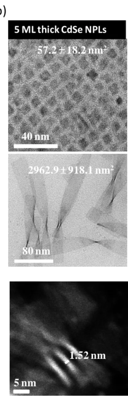
Among the NPLs of group II-VI semiconductors, it was observed that cadmium-based colloidal NPLs possess either wurtzite or zincblende crystal structure. Specifically, cadmium-based zincblende NPLs have ability to provide strong quantum confinement to the exciton confining in their ultrathin thickness and they have ability to grow in the lateral directions ranging from a few nanometers to a few hundred nanometers. Schematic representation of a zincblende 4 monolayer (ML) CdSe NPL is shown in Figure 2.4. A typical CdSe NPL is made up of cascaded monolayers of CdSe pair and it is terminated with Cd layer (100) on both the lateral sides [54]. Additionally, in order to show how successful the thickness and lateral size control of the NPLs is, the representative TEM images of 4ML and 5ML NPLs having both the small lateral size (with a few nanometers) and large lateral sizes (with a few ten nanometers) are given in Figure 2.5 together with the corresponding thicknesses ~1.2 nm and ~1.5 nm, respectively (1ML 0.3 nm).
15 40 nm 57.2 18.2 nm2 80 nm 2962.9 918.1 nm2
(b)
5 ML thick CdSe NPLs(a)
40 nm 105.3 16.4 nm2 160 nm 391.9 65.8 nm2 4 ML thick CdSe NPLs 5 nm 1.22 nm 5 nm 1.52 nmFigure 2.5. TEM images of (a) 4ML and (b) 5ML NPLs with both the small and large lateral sizes, and their corresponding thicknesses.
NPLs with cadmium-based zincblende structure have been extensively studied in terms of optical and excitonic properties [76]–[88]. It has appeared that these NPLs have several superior properties over the conventional CQDs. First of all, thickness control in three dimensions is not necessary for the NPLs; they require only one dimensional precise control in the thickness dimension where quantum confinement
16
happens. Therefore, cadmium-based zincblende NPLs possess spectrally narrow emission (FWHM < 10 nm) enabling very fine thickness-tunable PL in these nanostructures. An exemplary UV-Vis absorbance and PL emission spectra of 4 ML NPLs are shown in Figure 2.6. The absence of inhomogeneous broadening in these NPLs can be examined by comparing the PL FWHMs and time resolved fluorescence lifetimes for the single particle and for the ensemble of the particles. When this investigation is done, it is observed that there is not a significant difference in these two parameters of the cadmium-based zincblende NPLs. Furthermore, room temperature PL linewidth is slightly higher than 26 meV, which is the value of homogeneous broadening due to phonon coupling at room temperature. Extremely small PL linewidth of NPLs is highly desirable for color purity improvement under the context of LEDs.
17 2.4 2.8 3.2 517 443 388
Wavelength (nm)
UV-Vi
s
absor
bance/PL
intensity (
a.u.)
Energy (eV)
Figure 2.6. UV-Vis absorbance and PL emission spectra of 4ML CdSe NPLs.
The effect of strong quantum confinement on oscillator strength and thus the sharp absorption peaks in the nanoparticles has already been explained by using Fermi’s Golden Rule and Heisenberg’s Uncertainty Principle in the previous section (Section 2.1.1). As seen from the exemplary absorption spectrum of 4ML NPLs in Figure 2.6, as in the case of CQDs, NPLs have also sharp transition peaks in their absorption spectra. First peak is attributed to the transition due to the excitonic state of electron/heavy-hole pair; second peak corresponds to the electron/light-hole transition; and third peak is the transition forming the excitonic state between the electron and split off – hole [89].
Second advantage of these NPLs is that they have larger exciton binding energy than that of CQDs due to the combination of their 2D character, large in-plane charge effective mass and relatively smaller dielectric constant. Extremely large oscillator
18
strength and thus extremely fast radiative recombination lifetime in cadmium-based NPLs are important outcomes of their property of large exciton binding energy. While, at room temperature, the radiative recombination lifetime of these colloidal fluorescent emitters is a few nanosecond [79], it is around 10 ps at cryogenic temperatures [86], which is a strong implication of giant oscillator strength transitions in these NPLs. Large exciton binding energy and thus giant oscillator strength in the NPLs are important factors for enhanced per-volume linear absorption cross-section observed in these materials. The linear absorption cross-section along with the nonlinear absorption cross-section values of the NPLs have been recently obtained such that they are at least an order of magnitude higher than the corresponding values of CQDs [83], [84]. That much high absorption cross-section values of the NPLs allow them to be utilized for light-harvesting applications such as photovoltaics and photodetectors [90]. Additionally, they are potential exciton sinks due to their large extinction coefficient and thus the increase in the Förster radius aforementioned in the Förster theory [91].
Suppressed Auger recombination and thus long Auger lifetime is another advantage of the NPLs along with high close packing intensity and many other properties that were listed above for them to be utilized in low-threshold amplified spontaneous emission and lasing applications [79], [92]. Recently, these new nanostructures have also been used for the investigation of exciton kinetics in NPL based systems by using-FRET mechanism. Due to their superior excitonic characteristics both in absorption and emission features, high FRET efficiencies were obtained by using core, heterostructured and doped NPLs. All the advantages of cadmium-based NPLs are indicating that they are strong candidates to be used in next-generation light-harvesting and light sensing optoelectronic applications along with possible bio- and chemi-applications.
19
2.1.3 Layered 2D nanomaterials: graphene, graphene oxide,
reduced graphene oxide and MoS
2In the recent years, major scientific and technological challenges emerging in the fields of life science and nanoengineering have forced the scientific community to develop new materials. Carbon-based nanomaterials such as active carbon, carbon nanofibers, carbon nanotubes, graphene and graphene oxide have appeared as some of the key elements of the significant applications such as sensing, energy storage, energy conversion and transistor technologies along with the usage in catalysis and polymer composites [93]–[96]. Graphene, which is the monatomic layer of carbon, has particularly found some applications in optoelectronics [97] and biology [98], [99]. In addition, it has been offered as a new platform for the exploration of light-matter interactions at the nanoscale [100], [101]. Therefore, besides several experimental studies, many theoretical work has been conducted on the near-field interactions between an exciton donor and graphene [102]–[104]. On the other hand, graphene oxide (GO) along with its oxygen-reduced product, reduced graphene oxide (RGO), which are the variants of graphene, have been widely recognized owing to their exotic properties for several photonic, optoelectronic and biological applications.
Graphene is a single-atom thick, 2D hexagonal lattice of sp2-hybridized carbon atoms [105]. It was first produced through micromechanical cleavage [106]. Then, despite several advantages of this method in terms of purity, mobility and optoelectronic properties, for large-scale applications, the necessity of methods providing large-scale assembly of graphene appeared recently. For this reason, several approaches have been proposed and developed, and these approaches can be listed as follows: Liquid-phase exfoliation [107], chemical vapor deposition (CVD) [108], [109], physical vapor deposition (PVD), carbon segregation [110] and chemical synthesis [111].
Graphene has fascinating electrical, optical, mechanical, thermal and practical properties such as low sheet resistance, high transparency, broad absorption wavelength range, low cost, flexibility, high thermal conductivity and high chemical durability [112]–[115]. With these favorable properties, it has a great potential to be
20
used in photovoltaics as transparent conductor, photoactive medium, charge transport channel and catalyst; in LEDs as transparent and flexible conductive layer, in photodetectors as absorbing layer; in lasers as broadband and fast saturable absorber; and in various other photonic and optoelectronic applications [115].
Graphene films have some advantages when compared to the CQD films. The most important one is their better carrier transport properties including the high mobilities and their property of being large exciton sink [116], [117]. When their superior optical and electrical properties are combined with the exotic characteristics of CQDs and NPLs, novel nanotechnological devices may become enabled to be produced. Therefore, bringing these different systems together for their respective strengths and investigating the possible photonic and electronic interactions in their hybrids may allow opening a new scientific and technological research field. Upon the light of this perspective, in the recent years, many studies on FRET from CQDs and NPLs to graphene as well as various other luminescent materials to graphene have been reported [102], [118]–[123]. In these studies, for the detailed investigation of FRET mechanism, steady-state and time-resolved fluorescence spectroscopy techniques, which are elaborated in the Methods section, have been widely used. As an example for the FRET mechanism in graphene-based structures, a useful schema for the energy diagrams of an optical emitter and a nearby graphene monolayer film along with a representative sample structure is given in Figure 2.7, adapted from Ref. [124].
21
Figure 2.7. Energy diagrams of an optical emitter and a nearby graphene monolayer film along with schematic representation of the sample structure. (Reprinted with permission from Ref. [124]. Copyright 2013, American Chemical Society.)
Chemical structure of GO is very similar to graphene but having oxygen and hydrogen groups at its sp2- and sp3-hybridized carbon centers [125]. Production of solution-processed GO flakes was enabled after the invention of Hummers method by Hummers and Offeman in 1958 [126]. Reduced graphene oxide is another graphene-based nanomaterial, which is prepared from GO via several methods. For obtaining of RGO from GO or from graphite oxide, some of the methods that have been followed to date can be listed as thermal annealing [127], chemical reagent reduction [128] and multistep reduction [129]. When compared to pristine graphene, GO and RGO have some advantages such as greater aqueous solubility, ability to be functionalized with biomolecules, processing at lower cost, larger area coverage, and tunable energy bandgap [125], [130], [131]. Interestingly, GO can exhibit luminescence from localized electronic states rather than from band edge transitions [125]. Electrical conductivity of RGO is a direct measure of the success of reduction and, as a directly related parameter, the sheet resistance of RGO was reported as low as ~14 kΩ/sq [132], which is about two order higher than that of pristine graphene [105]. On the other hand, the highest bulk conductivity of a RGO sheet was reported to be 1314 S/cm, which is about two order lower than that of pristine graphene [133]. All these attempts for obtaining graphene-like RGO are highly remarkable and promising efforts.
22
In the family of graphene related materials, GO sheets are reported as fluorescence “superquenchers” having long range energy transfer characteristics, which makes them ideal candidates in FRET based applications [134]. FRET and charge transfer into GO or RGO, which have great potential to exhibit an energy quenching range comparable to graphene, are particularly important to explore and understand the feasibility and extent of being excitation energy sink [121], [123], [124], [135], [136]. Recently, several experimental studies have highlighted the importance of fluorescence quenching efficiency in the hybrids of QDs-GO [135], [137], [138], QDs-RGO [135] and dye-RGO [121] for the new developments in various application fields ranging from biology to optoelectronics.
In addition to graphene and its variants, transition metal dichalcogenide (TMD) crystals such as MoS2 and WS2 are also constituting another important group of
two-dimensional candidates to be used in the next-generation photonics and optoelectronics [139], [140]. Monolayer TMDs possess direct energy bandgaps ranging from near-infrared to visible spectral region, which is a significant property for them to be used in various photonic and optoelectronic devices and, thereby to fulfill the space of graphene due to its lack of an energy gap [140], [141]. Besides their direct bandgap property, TMDs share many other interesting characteristics of pristine graphene, such as excellent electronic and exceptional mechanical flexibility along with partial optical transparency. With these properties, they may have usage in electronic [142], optoelectronic [142] and nanophotonic applications [143]. These 2D nanomaterials can be obtained via mechanical exfoliation of bulk crystals built up of van der Waals bonded layers [106], CVD technique and many other techniques [142]. Van der Waals interactions between the layers of TMDs allow them to be grown with distinct semiconductors on each layer without a limitation originated from the lattice mismatch, which may lead to new heterostructures or superlattices [144].
Efficient FRET from localized chromophores such as 0D quantum dots to 2D TMDs has been reported in many studies conducted to date [145], [146]. Good FRET efficiency is directly dependent on a few factors including the spectral overlap between the donor emission and acceptor absorption, the distance between the donor and acceptor, the dielectric screening of the donor dipole by the acceptor medium and the
23
dimensionality [147]. Recently, two particularly important parameters have come into prominence for the efficient FRET to TMDs and graphene [118], [145]. These parameters are the extent of optical absorption and the extent of dielectric screening by the 2D exciton accepting material. Number of layers of TMD or graphene can mediate these two important factors in way that FRET rate increases with the number of layers in graphene but it decreases with the layer number of TMD, which is because of the competing effect of the amount of absorption and dielectric screening in TMDs and less effectiveness of dielectric screening in graphene [118], [145], [146]. For the next-generation optoelectronics, some concerns about the CQD films such as poor carrier transport can be overcome with the hybridization of these 0D chromophores with the newly emerging stars, TMDs, leading to higher mobilities [148].
2.1.4 Indirect bandgap 3D semicondutor materials: silicon
Silicon is the most commonly used and technologically important material in today’s industry. Its energy band structure having indirect absorption plays a very significant role in silicon based electronic, optoelectronic and photonic devices (see Figure 2.8). Because of the necessity of phonons for the optical bandgap transition, it needs to be treated more elegantly than the direct transitions. The bandgap of silicon has a value of 1.1 eV and its conduction band minimum is located around the point X of the Brillouin zone. When compared to the direct transitions, band edge absorption of silicon is very small because of its indirect feature and comparatively small density of states. Therefore, if the excitation energy is enough, the absorption spectrum is dominated by direct absorption at energies where the density of states is very high. Direct transition at minimum separation between the conduction band and valence band occurs near the L point and this transition is around the photon energy of 3.5 eV (~ 354 nm), which exhibits a peak shape in the absorption spectrum of silicon. Another important direct transition is around the energy of 4.3 eV (~ 288 nm), which is near the X point of the band structure [149].
24
Figure 2.8. Band structure of bulk silicon. (Reprinted with permission from Ref. [149]. Copyright 2001, Oxford University Press.)
Silicon is one of the most dominantly used materials in microelectronics and optoelectronics. Silicon based microelectronic technology has great potential for chips with features at sub-micrometer ranges. It also finds wide-scale utilization in optoelectronics, especially in photovoltaic industry. However, it has intrinsic optical constraints that limit the efficiency of photovoltaic devices. One important limitation of silicon-based devices is the decrease in responsivity in the UV region [150]. There have been numerous efforts to develop effective techniques to enhance the absorption in silicon. Some of these efforts can be listed as nanostructuring to trap the light, plasmonics to localize the light and using external light-harvesters via transferring the excitation energy in the harvesting material into silicon.
CQDs were proposed as efficient sensitizers for silicon owing to their favorable optical properties (e.g., efficient and tunable emission properties). Previously, CQD sensitization of silicon has been mostly facilitated via radiative energy transfer (RET) [151], [152]. Although RET based sensitization has achieved a considerable improvement in the conversion efficiencies of silicon solar cells, RET is fundamentally limited due to the lack of effective coupling of the emitted photons with the optical
25
transitions in silicon. Alternatively, FRET, which is a technique relying on mostly near field dipole-dipole coupling, has been shown to be feasible for sensitizer-silicon material systems [35], [153]–[155]. Previously, by using time resolved photocurrent spectroscopy, it was shown that CQDs are good candidates to facilitate the FRET into silicon [153]. Furthermore, steady-state and time-resolved fluorescence spectroscopy techniques were also used to investigate this energy transfer mechanism in CQD-bulk silicon hybrids [35], [155], [156].
2.2 Methods
2.2.1 Steady-state and time-resolved fluorescence spectroscopy
Recent years have witnessed major progress in steady-state and time-resolved fluorescence spectroscopy instrumentation. In addition, both the techniques have become powerful tools to study FRET dynamics [157], [158].In steady-state fluorescence spectroscopy measurements, emission spectra of the fluorescent donor and/or acceptor are obtained without temporal resolution (i.e. Intensity as a function of wavelength). Excitation is done at a fixed wavelength and scanning is performed over the wavelength spectra of the fluorophores. In the excitation part, xenon lamp with a monochromator or laser source is used. In the detection end, one of the most frequently used detector systems is photomultiplier tube (PMT), which enables to select different wavelength intervals and also it is the detection system what we use in our laboratory. Steady-state fluorescence spectroscopy allows to catch the spectral information over the wavelength range and thus to extract the FRET-related parameters along with the distances.
The analysis of steady-state fluorescence spectroscopy data requires careful treatment. For example, in order to have actual values of PL intensities from the samples, deconvolution of the spectra followed by the integration over each spectrum
26
is needed. On the other hand, for the well-separated spectra, peak intensity values are enough for the analysis of the spectral data. Also, the data from only-donor sample is not enough and it is important to obtain the information from both the donor and acceptor sides for the correct analysis. Detailed analysis of the PL data is necessary because the donor quenching can have become due to many reasons other than FRET but, acceptor sensitization, as the compelling evidence of FRET, together with donor quenching is a strong indication for the excitation of acceptor via donor and thereby the FRET [159].
Time-resolved fluorescence (TRF) spectroscopy method measures the fluorescence decay times at the time-domain or frequency domain. Generally, we do time-dependent measurements in our laboratory; therefore it is necessary to elaborate these measurements more carefully in this part: TRF spectroscopy is the measurement of luminescence intensity as a function of time and following a short pulse of light excitation. The decay time of the sample has to be much longer than the excitation pulse. Logic for operation of the TRF system is given in Figure 2.9.
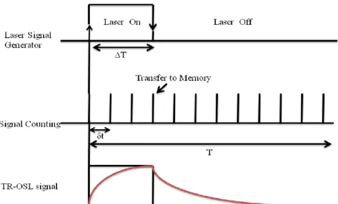
In the TRF experiments, first, the laser is opened for a short stimulation time of ΔT and the signal counting is started simultaneously. Data acquisition is performed with time intervals of δt. The data is transferred to memory at the end of each δt. Following the time of ΔT, laser stimulation is terminated but data acquisition and storage to memory still proceed. In general, after a period of time T for completing the laser on and laser off periods, the accumulation process has to be repeated to accumulate the data over and over for high signal to noise ratio. The form of TRF signal obtained during and after the stimulation is shown in the following figure. We use the intensity decaying curves from the TRF spectroscopy to obtain the excited state excitonic lifetimes of various nanostructures.
27
Figure 2.9. Logic for operation of the TRF system.
Typically, we use a time correlated single photon counting (TCSPC) system in the laboratory having a time resolution down to 4 ps (PicoHarp 300) integrated with a picosecond pulsed laser with an output photon energy of 3.31 eV driven by a driver module (PDL-800 series) capable of delivering laser pulses with 80 MHz repetition rate. The system utilizes a fast PMT (Hamamatsu H5783 series) to resolve lifetimes on the order of tens of picoseconds. Also, we integrate a close cycle Helium cryostat to this system in order to do temperature dependent studies. The whole system with its complementary components is shown in the Figure 2.10 and Figure 2.11.
28
Figure 2.10. FluoTime 200 TRF system.
![Figure 2.8. Band structure of bulk silicon. (Reprinted with permission from Ref. [149]](https://thumb-eu.123doks.com/thumbv2/9libnet/5949035.124040/41.892.269.655.198.486/figure-band-structure-bulk-silicon-reprinted-permission-ref.webp)