4:00pm-4:15pm
ML2
High-speed 1.3 pm GaAs Based Internal Photoemission
Resonant Cavity Enhanced Photodetector
Ibrahim Kimukin, Ekmel Ozbay
Department of Physics, Bilkent University, Bilkent, Ankam 06533, Turkey
Necmi Biyikli, Tolga Kartaloglu, Orhan Aytur
Department of Electrical and Electronics Engineering, Bilkent University, Bilkent, Ankara 06533, Turkey
Gary Tuttle
Microelectronics Research Center, Iowa State University, Ames, IA 5001 1
High-speed infrared photodetectors are becoming increasingly important for optical communication, signal processing, infrared imaging, and measurement systems. RSi and IrSi Schottky contact internal photoemission detectors for operation in the infrared regions are among the most promising sensors for large-scale monolithic infrared imaging arrays due to their compatibility with the standard Si or GaAs integrated circuit processing.
Resonant cavity enhanced (RCE) photodetectors offer the possibility of overcoming the low quantum efficiency limitation of conventional photodetectors[l]. The RCE detectors are based on the enhancement of the optical field within a Fabry-Perot resonator. The increased field allows the use of a thin absorbing layer, which minimizes the transit time of the photogenerated carriers without hampering the quantum efficiency. High- speed RCE photodetector research has mainly
concentrated on using pi-n photodiodes and avalanche photodiodes, where 75 % quantum efficiency were achieved along with a z 20 GHz
bandwidth[2]. Recently, we fabricated high-speed RCE p-i-n and Schottky photodetectors, where a
90\% quantum efficiency along with a 3-dB
bandwidth of 50 GHz and has been reported[3].
4 -1
...
metal
semiconductorFig. 1. Internal photoemission mechanism in the Schottky metal.
Internal photoemission is the optical excitation of electrons in the Schottky metal to an energy above the Schottky barrier and then transport to the conduction band of the semiconductor as shown in Fig. 1. According to the theory developed by Fowler, the number of electrons emitted per quantum of light absorbed is to a first approximation proportional to the number of electrons per unit volume of the metal whose kinetic energy normal to the surface is sufficient to overcome the potential step of the surface[4]. The internal quantum efficiency in the vicinity of the cut-off wavelength is given by:
Here c p ~ is the Schottky barrier height. The external quantum efficiency can be found by multiplying the absorption in the Schottky layer and the internal quantum efficiency.
I l i E hV-cpB 9 (hV>cpB)
0-7803-5947-X/00/$10.0002000
IEEE
108
Fig.2. Diagram showing the cross section of a fabricated photodiode
We used the transfer matrix method to design the epilayer structure and to simulate the optical properties of the photodiode. The samples were fabricated by a microwave-compatible process. The crossection of a fabricated photodiode is shown in Fig. 2.
Photoresponse measurements were camed out in the 1100-1500 nm range by using a single-pass monochromator and a tungsten-halogen projection lamp as the light source. The monochromatic light was delivered to the devices by a lightwave fiber probe, and electrical characterization was camed out on a probe station. The spectral response was measured using a calibrated optical powermeter. Figure 3 shows the spectral room temperature
quantum efficiency measurement and theoretical calculations at zero bias.
fi
006 ::
. I
1100 1200 1300 1400 1500
Wavelength (nm)
Fig. 3. Measured and' simulated quantum efficiency at room temperature at zero bias.
10 l2
/----T-
I
I
I \
0 50 100 150 200 250 l i m e (psec)Fig. 4. Temporal response of the 100 pm2 area
RCE Schottky photodiode at the resonant wavelength.
I
I
1
F~~~~~~
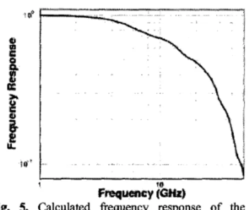
Fig. 5. Calculated frequency response of the photodiodes
High-speed measurements were made with an optical parametric oscillator (OPO)[5]. The OPO is based on periodically poled KTP crystal with a 24
pm poling period. Our OPO is pumped by a mode- locked Tisapphire laser operating at the wavelength of 762 nm. Pump pulses were 215 fs in
duration and had a repetition rate of 76 MHz. The setup produced pulses at 13 10 nm with a FWHM pulse width less than 1 ps. Figure 4 shows the temporal response of a small area (7 pm x13 p)
photodiode measured by a 50 GHz sampling scope
at zero bias. The Fourier transform of the measurement data had a 3-dE3 bandwidth of 20
GHz as shown in the Fig. 5. Diodes were RC time limited due to very thin intrinsic GaAs layer with expected bandwidth of 70 GHz. The discrepancy between the expected values and the measurements was mainly due to the laser timing jitter which broadened the measured pulse width. To our knowledge, these results correspond to the first high-speed intemal photoemission photodetectors.
References:
[l] M. Seiim Unlu, Samuai Strite, J. Appl. Phys.
[2] H. Nie et. al., Appl. Phys. Lett. 70, 161, (1997). [3] E. Ozbay et. al., Appl. Phys. Lett., 74, 1072, (1 999).
(41 R. H. Fowler, Phys. Rev. 38,45, (1 93 1) [5] T.Kartaloglu et. al., Optics Lett. 23,61, (1998). 78,607- 638 (1995).