s
AMER I c AN Copyrighl © 2017 by American Scientific Publishers SCIENTIFIC All rights reserved.
PUBLISHERS Printed in the United States of America
Journal
of
Nanoelectronics
and Optoelectronics
Vol. 12, pp. 109-117, 2017
www.aspbs.com/jno
Microstructural Analysis with Graded and
Non-Graded Indium in lnGaN Solar Cell
ilknur Kars Durukan 1·*, Mustafa Kemal 6zturk 2·3 , S(.ileyman <;orekc:;:i4, Mehmet Tamer3·7, Yunus Ba~5, Suleyman 6zc:;:elik2·3 , and Ekmel 6zbay 6
In this study are graded and non graded lnGaN/GaN samples grown on c-oriented sapphire substrate using the Metal Organic Chemical Vapour Deposition (MOCVD) technique. The structural and morphological prop-erties of the grown lnGaN/GaN solar cell structures are analyzed using High Resolution X-ray Diffraction (HRXRD), atomic force microscopy (AFM). Each structures
c
anda
lattice parameters strain, biaxial strain,hydrostatic strain, stress, lattice relax, tilt angle, mosaic crystal size, dislocation densities of GaN and lnGaN layers are determined by XRD measurements. In accordance with these calculations, the effect of graded structure on the defects, are discussed. As a dramatic result; although values of full width at half maxi
-mum (FWHM) are broad, a considerable decrease at dislocations is noticed. The AFM observations have revealed that the two dimensional growth of the graded sample is more significant and its roughness value is lower. JV measurements shown that the performance of the graded structure is higher. It is determined that all test results are consistent with each other.
Keywords : lnGaN/GaN Solar Cell, MOCVD, HRXRD, AFM.
1
.
INTRODUCTION
Recently, group III-nitride wide semiconductors band gap has led to the development of light emitting devices and high efficiency solar cells_ 1- 5 Furthermore, InGaN alloys have become subject to an increasing research effort because of its high carrier mobility, high drift velocity, and durability in high-temperature and radia-tion environments. All of these are necessary to p ro-duce high efficiency solar cells_6-io However, the growth of a high crystal quality GaN/lnGaN solar cell stru c-ture is difficult because of the large difference in the
1 Life Sciences Research and Application Center, Gazi University, Golba~,. Ankara, Turkey
1 Department of Physics, Faculty of Sciences, Gazi University, Ankara, Turkey
3Photonics Research Center. Gazi University. 06500 Ankara, Turkey 'Energy Systems Engineering Department. Faculty of Technology, K1rklareli University, Kirklareli, Turkey
;National Boron Research Institute, 06520, Ankara. Turkey
'Department of Physics, Bilken1 University 06800, Bilkent. Ankara. Turkey
7Depanment of Physics. Zirve University, Gaziantep, Turkey • Author 10 whom correspondence should be addressed. Email: [email protected]
Received: 18 March 2016 Accepted: 18 May 20 I 6
suitable coefficient of thermal expansion (28% GaN and InN) and the lattice disconformity ( I 0.6% GaN and lnN) between films and substrate. For the III-nitrides, especially InGaN grown on a GaN template, graded buffer layer is used to improve the quality of the epilayer. However,
there are only a few reports researching the continuously graded buffer layer11· 12 and thus this buffer layer tec h-nique has not been accurately understood. The purpose of this study is to report the results for In graded In.rGa1_.rN (10.5 .:::
x.:::
18.4) and non-graded In,Ga1_,N (13.6 .:::x .::: 24.9) epitaxial structures obtained by using metal organic chemical vapor deposition (MOCYD). We have investigated the graded interlayer technique for impr ov-ing of the InGaN epilayer quality on sapphire substrates. Our study found surface and volume defects such as strain, hydrostatic and biaxial strain components, stress,
the plane tilt angle, mosaic crystal size, heterogeneous strain, dislocation densities and surface morphology via mosaic crystal model. In addition, the effects of graded layers on different type of dislocation densities are d is-cussed with XRD measurements. The atomic force micro -scope (AFM) has been used for observing the surface morphologies of the films and their roughness. Further, Current density, potential (JV) measurements and the solar battery performance of the grown structures are discussed.
Microstructural Analysis with Graded and Non-Graded Indium in lnGaN Solar Cell Ourukan et al.
2. GROWTH CONDITIONS
ln the present study, InGaN/GaN solar cell structures (Fig. I) were grown via the MOCVD technique on
c-oriented sapphire substrates. When sample A was deposited as graded, sample B was deposited as non -graded. Prior to the growing process, substrates were cleaned under H2 gas to eliminate the contaminations on the surface. After the decontamination procedure, for each
sample, a GaN nucleation layer was grown. The thickness of this nucleation layer was IO nm. Followin g the comple-tion of the nucleation layer growth, the GaN buffer layer was grown. The thickness of the GaN buffer layer was 1.6 µ,m. The growing process was endured by releasing the SiH4 source and an 11-type GaN layer was obtained with the aid of the SiH4 source. Furthermore , the flow rate of the SiH4 source was IO seem. The InxGa1 _xN
active layers were grown for samples A and B at temp er-atures between 745-760 °C degree and an In flow rate of
75 seem. While the InGaN layer thicknesses in sample A were 25 nm (graded) and 200 nm (graded) , the InGaN layer (non-graded) had a thickness of 220 nm. The active
layers were grown between 1.9 µ,m thick ,Hype GaN and p-type InGaN contact layers.
The p+ InGaN layer was grown by using a Mg doping source. The Mg flow rate was adjusted to 40 seem to p ro-vide more doping. The InGaN layer was converted to a graded status by keeping the InGaN layers's in flow rate continuous.
p contact lnGaN layer
p contact lnGaN layer
graded lnGaN layer
nongraded lnGaN layer
n contact GaN layer
non doped layer
non doped layer
non doped layer
non doped layer
non doped layer
Low Temperature GaN nucleation layer(2.45 min)
Sample A
3. RESULTS AND DISCUSSION
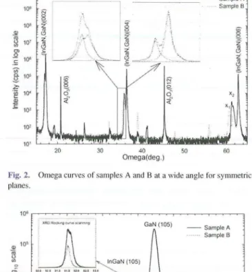
3.1. XRD AnalysisOmega curves of samples A and B at a wide angle and diffraction peaks of InGaN and GaN for all symmetr ic diffraction planes are defined (Fig. 2). The layers of InGaN and GaN are repeated as triple peaks (or sets). These peaks match up to (002), (004) and (006) symmetric planes of hexagonal crystal structure , respectively. For both samples,
the peaks of GaN coincide with those of in case of strain-free. Besides, low severe azimuth peaks belonging to GaN and Al2O3 can be observed. The peaks with high intensity and low FWHM of lnGaN show that they are of high qual-ity. For sample A, the peaks show continuity depending on In ratio of graded InGaN layer (Fig. 2 inset). For sample B, two different peaks as x1 and x2 alloy rates of InGaN are observed depending on the rate of In. On the other hand, X-ray diffraction peak from asymme tric planes ( I 05) is examined to investigate quality of the crystal structure (Fig. 3). In addition, peak of In graded InGaN and two peaks of In non-graded InGaN are observed. The (004) peak for every two samples is separated with InGaN's two omega peaks in the inset of Figure 3. High intensity and lower FWHM values verify that the crystal quality is high
(Table I). Otherwi se, the asymmetric peak positions and FWHM are used for calculations of lattice parameter and mosaic defects of hexagonal structure.
Nitrogenous compou nds and alloys like GaN, InGaN are in hexagonal structures. The crystal quality decrease s
p contact lnGaN layer
p contact lnGaN layer
nongraded lnGaN layer
n contact GaN layer
non doped layer
non doped layer
non doped layer
non doped layer
non doped layer
Low Temperature GaN nucleation layer(2.45 min)
Sample B
Fig. 1. lnGaN layered solar cell structure (a) In graded sample A, (b) Non In graded sample B.
Durukan et al. Microstructural Analysis with Graded and Non-Graded Indium in lnGaN Solar Cell ,010 1()' 10' .91 B 107 </) Ol .Q 10' .!: u, ~ 10' ~ .iii 10' C ~ J; \()' 10' 10' Fig. 2. planes. W 10!,
13
</) 0t
10' . !: u, a. u :; 103 ·;;; C Cl) E 10' N 0 0 ¥ \ "' <.!) z 0 £ 20 30 _______ -- Sample A Sample B 40 0mega(deg.) 50 60Omega curves of samples A and B at a wide angle for symmetric
GaN (105) lnGaN (105) 100 102 104 106 20 (deg.) - Sample A ··· Sample B 108 110
Fig. 3. 20 curves of samples A and B at wide angle for ( I 05) planes.
when the symmetri c peaks are broadened. The broadening
of the symmetric and asymmetric peaks for these type
of layers are noticed by the change in plane tilt, twist angles and the lateral crystal sizes parallel with the sub -strate surface.
FWHM values of sample A except for GaN (004) value are found to be wider than those or sample B. The sp lit-ting of sample B cannot be observed because sample A has
graded structure (Fig. 2). Therefore , a large amount out of the FWHM value in sample A depends on the constant ofln
ratio. For example, this FWHM value is the 890.64 arcsec
unit and belongs to InGaN (004) for sample A, which is
the expected value according to InGaN structure.
According to the Yegard's law. the ratio of the alloy in InGaN layer depends on the peak positions of InN and GaN. When the x value of InGaN is different from what it is supposed to be, the Yegard's law is used for calcula-tion. However, to differentiate the strain value appendage of lnGaN at x value, the cubical equation of Ax3
+
Bx2+
Cx+
D= 0 can be
used.13 A, B, C and D coefficients ofthis cubical equation includes InN, universal a and c lat-tice parameters of GaN and Poission ratios. x ratio can be solved using a program in 0-1 interval, and qualities such as strain and relax are calculated, afterwards.
Ge 022
(+
, -, -,
+)
monochromator and GoebbelsmirTor were employed to separate ka 1 and ka2 in the
parallel sheaf and to eliminate ka2 in the HRXRD
technique. The measurements of the symmetrical and
asymmetrical reflections, Bragg angle 8 and lauice curving angle T can be calculated through the 8
=
(8
+
+8
_
)/2
and T=
(8
+
+8
_
)/2
equations.14 a and clat-tice parameters of corrupted InGaN hexagonal unit cell are calculated from a proper angle of the hk (-h-k )/ re flec-tion. Three different techniques could be used to calculate the lattice parameters. For the first technique, the lattice parameter of the InGaN, by taking the Yegard's law into
consideration , is found by adding x numbered InN lallice
parameters to ( I - x) numbered GaN lallice parameters .
To obtain a and c lallice parameters on the asymmetrical planes, by means of using sin T and cos T at the denomi -nator of the equations below, the second technique can be procured.15 A.I C= - --- -2sin8 COS7 A./4f!,J h2
+
hk+
k2 a=-- - ---2 sin 8sin T(
1
)
(2)For the last technique, using the ( I -
D
cos28)
/
(
r
sin8)
error function and Bragg Law, the parameters could be calculated by; IA c= - -x 2sin8
(error function) (4/3)( h2+ k2
+
hk) c2 - /2c/7ikl (3) (4) Equations (3) and ( 4 ). 16 On the error function , D is thepossible displacement of the sample with goniometer axis
on asymmetrical plane (equatorial plane), and its value
is 0.02. R, which is the distance of the sample from the
detector (450 mm).
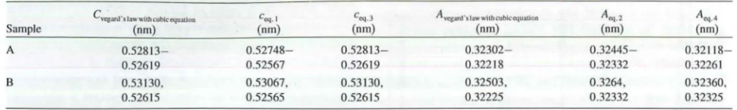
The lattice parameters of InGaN graded solar cell
(sam-ple A) are given as value ranges (Table II). The reason for
Table I. Peak broadening of (004), (105) diffraction planes of InGaN and GaN in arcsec unit. Sample A B lnGaN (004) 890.64 (550.08, 542.52) J. Nanoelectron. Optoe/ectron., 12, 109-117, 2017 lnGaN (105) 2271.96 (1679.40, 1606.30) GaN (004) 285.12 300.60 GaN (105) 859.68 804.24 111
Microstructural Analysis with Graded and Non-Graded Indium in lnGaN Solar Cell 0urukan et al.
Table II. The c-and a-lattice parameters found through Vegard's law, Vegard's law with cubic equation and error function on InGaN layer(s) for all
samples and their comparisons.
C,-egard'slaw"ithrublcequaLioo ceq.1 ccq.J Avcgan1 'slaw with cubicequalion Aeq.2 Acq.•
Sample (nm) (nm) (nm) (nm) (nm) (nm)
A 0.52813- 0.52748- 0.52813- 0.32302- 0.32445- 0.32
118-0.52619 0.52567 0.52619 0.32218 0.32332 0.32261
B 0.53130, 0.53067, 0.53130, 0.32503, 0.3264, 0.32360,
0.52615 0.52565 0.52615 0.32225 0.32332 0.32325
this behavior is broadening of InGaN reflection as a
conse-quence of increased In ratio. Lattice parameters are given
as different two values for the non graded InGaN solar
cell (sample B). Correction function is applied for the la
t-tice parameters in Eqs. (I) and (2) because peak intensity
observed in large Bragg angles is far away from linearity.
The absolute lattice parameters were obtained using
cor-rection functions (3rd and 4th equations). Accordingly,
the lattice parameters obtained with cubic equations and
Vegard's law match the lattice parameters obtained by
error calculations.
The point and line defects of GaN layer cause
direc-tional shifts on the lattice, and the shift leads to minute
deviations on the peak. The distance between strain planes
is directly related to the lattice parameters and to the
ratio of In. Moreover, the strain risen as the polar angle
increases and the square of the sinus of the angle provides
a definition for the strains on the lattice. If these strains are
gradient, they must have three axes, and in this case there
must be a component of the surface-normal strain. A strain can be calculated using the base plate or its universal
val-ues. Here, the strain is calculated using the universal values
of InGaN and AIGaN. The strain equation can be given as
8d 8a 8c
- - - =80co t0
d '
a
'
c
with its error function.15
(5)
On two dimensions, biaxial strain is known as lattice
stressed or strained. Lattice strain is the sum of the biaxial
strain components on two dimensions and the sum of the
hydrostatic components on three dimensions. The compo
-nents of biaxial and hydrostatic strain are as follows:11-19
(6) C33£,-
+
2C13£" £1,=
2C13+
C33 (7) When strain values are between (0.995 - 1.23) x JQ-3ranges for sample A, they are (0.995 - 1.80) x I 0-3 ranges
for sample B (Table III). The second InGaN peak of sa
m-ple B is overlapped with the right edge of the graded
InGaN peak of sample A (Fig. 2 inset). Thus, strain
values are obtained as the same values. While a-strain
values of sample A are [(- 0.441)- (- 0.353)]
x
10-3ranges, they are [ ( - 0.429) - ( - 0.33 I)] x 10-3 ranges.
These values show that hexagonal lattice of sample A
is more compressive strain. While the crystal lattice of
sample A in c direction for the two dimensional strain
values is more extensional, it is more compressive in
a direction. Two dimensional strain values are given in
Table III. IL is seen that hydrostatic strain values result
-ing from point defects is more compressive in InGaN
crystal structure. Hydrostatic strain values are given in
Table III.
Alloy structures on hydrostatic strain are affected by
doping and point defects. Depending on the size of the
strain defects, the lattice can be compression or tensile.
Different types of point defects might emerge, depending
on the growth conditions. In general, it can be expected
that the effective hydrostatic strain in GaN originates from
AIGa• N1n, Ga1n, NGa substitutional type point defects, N;,
Ga;, Al; and In interstitial point defects, V1n and V Ga
vacancies Refs. [20, 21] The covalent radius of the Al
(1.43
A)
can come from Al203 , Ga (1.22A)
and In( 1.63 A) atoms are considerably larger than the covalent
radius of the N (0.70
A)
atom. Covalent values can beeasily found in textbooks or in some other way. Therefore,
AIGa• GaN InN, Al , InGa• lnA1, In;, Ga;, Al; and N; type
defects cause a crystal lattice expansion, whereas GaAI•
NGa• Nin• NAI• Gain• Alln• VAi• VGa• Vin• and VN type point
defects lead to crystal lattice compression. In our case,
we find that the hydrostatic strain in first two temp
era-ture values of the lnGaN layer is of compressive character
and large by absolute value (Table VI). Therefore, we s
up-pose that the relative concentrations ofGaAI• NGa• N1n, NAI•
Ga1n, Al1n, V Al• V Ga• V1n, and V type defects are dominant
in other types of point defects. Table Ill. a- and c-lattice strains, a-and c-biaxial strains, hydrostatic strain in InGaN layers of all the samples.
Sample A B 112 c-strain nm (x 103 ) 1.23-0.995 1.80, 0.995
a-strain nm Biaxial strain c
(x 10-3) (x 10-3)
(-4.4 1)-(-3 .53) (2.47}-( 1.99)
(-4 .29), (-3.31) (2.37), (1.87)
Biaxial strain a Hydrostatic strain
(x 10-3 ) (x 10-3)
(-3.18)-(-2.53) (- 1.20)-(- 0.995)
(-3.1 I), (-2.38) (- 1.18), (-0.930)
Ourukan et al. Microstructural Analysis with Graded and Non-Graded Indium in lnGaN Solar Cell
Table IV. Stress x, y, z and stress size of lnGaN. Sample A B x-stress (Gpa) (-1.33)-( 1.04) ( - 1.35), (0.97)
y-stress (Gpa) (- 1.35)-(1.05) (-1.37), (0.98)
On the epitaxial layer, the internal plane strain can be calculated using the equations below, if the a-oriented biaxial strain and the material elasticity constants are
k_nown.19.22
(8) Here, the information in the parenthesis 1s labeled as biaxial module (M 1 ); hence, the biaxial strain is shown with <T
=
M s1' 19f f a·
The magnitude of stress is obtained by using stress com -ponents (Table TV). When the sizes of stress for sample A changes between ( 1.80-2.3 I) GPa ranges, the values of (1.69, 2.35) GPa are observed for sample B. Thus, it is seen that the stress components are about same sizes for the two samples.
Strain relax is defined as the percentage of the ratio of the difference of relaxed lattice length between layers and substrate layers to the difference of universal lattice lengths, and it is represented with the equation below.15
L(means) S(means)
all - all
R'lr
=
--"--L~ (O_)_---'!.S-(0-) - X 100all - all
(9)
Lauice structure of sample A has more relaxation than that of sample B (Table V).
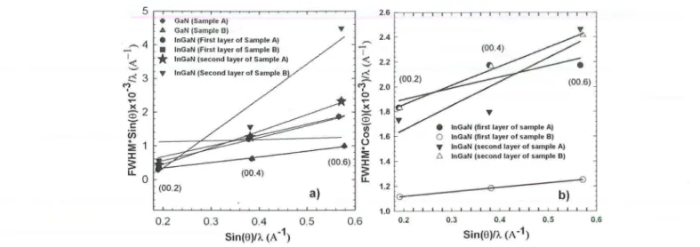
The symmetric plane is the plane which intersects the normal of the surface. Assuming that the sample plane is initially in the z direction, if this plane diverges with an angle to the z axis, creating a surface angle, there will be a crystal plane with observed asymmetric diffraction. The incident and reflected wave vectors used to provide the interference of these planes are to ensure the Bragg diffraction conditions. If a symmetric diffraction cause the lateral crystal size of the mosaic blocks and the plane tilt angle failure the expansion of the HRXRD twist curves
which are vertical to the pole axis. 23 The expansion of the reflection plane used to differentiate between both defects is defined by a linear equation. The Williamson -Hall (W-H) study can be used for this purpose.23 The W-H graphic is the FWHM graphic of the HRXRD twist curve as a function of the reflection plane level, meaning that
Table V. Lattice relax of lnGaN layers in the samples.
Sample Lattice relaxation (%)
A 1.34783-1.34826 B 1.22875, 1.32033 J. Nanoelectron. Optoelectron., 12, 109-117, 2017 z-stress (Gpa) (-1.32)-(- 1.03) (- 1.34), (-0.97)
Stress size (Gpa) 1.80-2.31 1.69, 2.35
each reflection is FWHM (sin 0)/ ,\ drawn against (sin 0)/ ,\ and the drawn curve is quitted with the linear equation.
The W-H curves for the GaN buffer, InGaN contact and active layers for A and B solar cell samples are shown in Figure 4(a). Where the FWHM measures for maximum half-width peaks; ,\ and 0 are the X-ray wave length and Bragg angle respectively. Meanwhile the plane tilt angles for GaN and InGaN are determined from the inclination of the lines seen in the Figure 4, the lateral mosaic sizes
L11 are obtained from the points which section they axis.
The lateral crystal sizes and tilt angles obtained from
the W-H curves for the GaN buffer, InGaN active and con-tact layers are shown in the fourth and sixth columns of Table YI. The data related to the structural features of GaN are separated in the table with a comma from those of the InGaN layer and the "/" symbol is used for the InGaN
layers. The lateral crystal sizes and tilt angles for the GaN buffer layers in A and B InGaN solar cell samples provided the same values. This situation shows the same growing conditions at MOCVD for both samples. In comparison,
the InGaN layers of both samples have lateral mosaic cry s-tal sizes, and similar behavior like that of GaN. Further
-more, it is seen that the plane tilt angles of the second InGaN layers of samples had the same value. In addition to this similarity, there are some differences determined between the mosaic parameters of these InGaN layers. The
lateral mosaic crystal length of the second InGaN layer and the plane tilt angle in the first InGaN layer of sam -ple A had a lower value than those of the same layers in sample B. when the tilt in the graded structure is compared with non-grade structure, a significant difference does not exist. The reason for this is because the insertion of graded interlayers has more effect on twist than the tilt.24·25
Furthermore, this result had a negative effect on the
crystal size, for it decreased the plane angle. When com
-paring the crystal sizes and the layer tilt angles of the interior lnGaN layer of each sample, it was determined that the crystal sizes of the buffer layers were greater but more imperfect due to the higher plane tilt angle.
A vertical mosaic size and an c-axial combined strain in the radial scan direction of symmetric reflections cause an increase in FWHM values of the Bragg reflections. In the W-H graphic23 a counter graphic of FWHM (cos 0)/ ,\ versus (sin 0)/,\ is drawn for each reflection and a linear output is performed in Figure 4(b ). The vertical mosaic dimensions L1. are determined by Eq. (10) from the y0 section point of the obtained line.
L1.
=
0.9/(2y0) ( I 0)Microstructural Analysis with Graded and Non-Graded Indium in lnGaN Solar Cell Durukan et al.
5
•
GaN (Sample A)A GaN (Sample B)
•
lnGaN (First layer of Sample A),.-..4
•
lnGaN (First layer of Sample B)I
*
lnGaN (second la~r of Sample A) $~3
...
lnGaN (Second layer of Sample BM 'o ...
.g,
2c
'!' ~ ::cs:
u.. 0 (00.2) 2.6...
2.4 I $ 2.2 ~ M 2.0 b ... ~ 1.8 $' VJ 0 1.6u
:i:
:I: 1.4~
a) 1.2 1.0G--lnGaN (firsl layer of sample A) lnGaN (first layer of sample B)
T lnGaN (second layer of sample A)
6 lnGaN (second layer of sample B) (00.6)
___ --e-e --~ ---0
b) 0.2 0.3 0.4 0.5 0.6 0.2 0.3 0.4 0.5 0.6
Sin(0)n.. (A- 1) Sin(0)/).. (A •1)
Fig. 4. Williamson-Hall graphics for the GaN. active and contact lnGaN layers.
In the tilt of the obtained lines created from pe rform-ing linear outputs by drawing FWHM (cos 0)/ ,\ versus (sin 0)/ ,\ for each reflection in the W-H graphic are the
determined heterogeneous strain values and the obtained
vertical mosaic sizes regarding lnGaN solar cell samples
A and B (Table VI, column 3 and 5).
The vertical mosaic crystal size for the GaN layers
of both samples provided the same experimental result,
although the vertical mosaic crystal sizes for the InGaN
layers have shown a different behavior. The vertical mosaic
crystal sizes in the InGaN layers of the preliminary layer in sample A are lower than those of the Preliminary layer in
sample B. However, this shows the exact opposite
behav-ior of the collateral InGaN layer in samples A and B. Similarly, the same is observed on the preliminary and
preliminary InGaN layers of samples A and B.
The vertical mosaic crystal size of the collateral
prelim-inary of sample A was higher than that of the preliminary
layer, the vertical mosaic crystal size of sample B's first
layer was higher than that of the collateral layer (Table VI). The bulk of mosaic crystal size is due to the calibration trend of the MOCYD, though In contents of InGaN and
layer thicknesses are different, yet this is related to the crystal quality of the layer.
The heterogeneous strains obtained for both samples are
shown in the third column of Table VI. The heterogeneous
strains of the GaN and InGaN layers of sample A are
Table VI. Mosaic defect features of samples A and B.
In Heterogenous Lateral
Samples GaN Content Strain mosaic
InGaN/lnGaN (%) (x I0-4) size (A)
A (graded) 10.5/18.4 -3.75, 2.25/4.75 9000, 900/250
B (non- 13.6/24.9 -4.00, 1.0/3.75 9000, 900/265
graded)
114
slightly higher than those of sample B. It is determined
for the InGaN layer that the heterogeneous strains of the collateral layers of samples A and B are higher than those of the preliminary layers.
A method regarding the calculation of the edge and
screw dislocation is based on the Burgers vectors as
well as both the till angle and the lateral mosaic sizes. All types of dislocations are related to the mosaic crys -tal sizes, tilt angle and the twist angle. Metzger et al.26 stated that edge type dislocations with a mean twist angle
Burgers vector b
=
l /3 ( 1 I - 20) and screw type dislo-cations with a mean tilt angle Burger vector b
=
(000 I)(TDD) are related to each other. The intensity of the
screw type dislocation density can be calculated by using
Eq. (II ).23 21-30 ? N a;;11 screw=
-l
b
1
2
screw (II)Here a,il, is a tilt angle for GaN and bscrew
=
0.5185 nm.The Burgers vector equals the lattice parameters. There
-fore, the Burgers vector of the InGaN layers is ca
lcu-lated using Yegard's law. The bscrcw value of the lnGaN
layers for sample A is determined to be 0.5240 nm
and 0.5281 nm, and for sample B to be 0.5256 nm
and 0.5315 nm respectively. Edge type dislocations co
n-vert consistently with the azimuthal rotation of the cr
ys-tals around the surface normal by the Burgers vector
Vertical Tilt Screw TDD Edge TDD
mosaic angle (x 104, (x 106 ,
size (A) (x 10-3 ) (Deg.) 105/106) (cm-2) 107/107) (cm-2) 321, 265/346 1.70, 4.2/1.03 7 .51, 4.43/2.68 5.50, 0.806/290 321, 450/281 1.70/ 5.0/1.03 7.51, 6.56/2.82 5.56, 1.06/361
Ourukan el al. Microstructural Analysis with Graded and Non-Graded Indium in lnGaN Solar Cell
b
=
1 /3( 11 - 20). The edge type dislocation intensity can be calculated by the measured a,wis, twist angle. The edge type dislocation intensity can be calculated by Eq. (12)when the dislocations in the structure· accumulate within
the low angle grain boundari es.30·31
( 12)
Where a1, is the half-width peak of the asymmetric plane
is related with twist. Burgers vector value is 0.3 l 89 nm for GaN, and L11 is the lateral CL. For lnGaN layers in sample A bE are obtained as 0.3226 and 0.3253 nm, and
0.3237 and 0.3276 nm for the layers in sample B. The
edge and threading dislocation s of samples A and B are obtained in Table I. The edge and threading dislocation values of the GaN layer in both samples have an almost equal value. It is seen that both the edge and the threading
dislocations of the InGaN layers are lower in sample A. In previous presented studies, the insertion in the graded layer significantly reduces the edge and screw dislocation densities have been reported.24 It is observed that sample A
has a more qualitative structure.
The FWHMs of w and </J scans are determined by fit -ting to the Pseudo-Voigt. In this fitting, the FWHM s of
w-scans increase due to scaling up of the
x
angle and the FWHMs of ¢-sca ns decrease due to the increase of thex
angle. Besides, the w and ¢-scans ( 12. I) coincide with each other at reflectionx
31 at 78.6°. In fact, thex
angle reaches 90° when the reflection plane isverti-cal to the sample surface. According to these results, the
HRXRD rotating peak widths of w or </J scans for this high
x
angle are similar to their twist angles. In any case,the FWHMs of the ¢-scans are greater than those of the
cu-scans when a change in the
x
angle occurs . Therefore,the mean twist angle of
x
=
78.6° needs to be the meanvalue of the FWHMs of the w and
<p
scans. The twist angles of GaN are determined as 0.118° and 0.141 ° for samples A and B respectively. 32-34 It is seen that the value of sample B is slightly higher than that of sample A. Forthe InGaN layers, the image of the twist angle ( 12.1) was
unable to be solved due to the reflection peaks of the plane remained in the background. 35
0.00 nm 0.00 nm
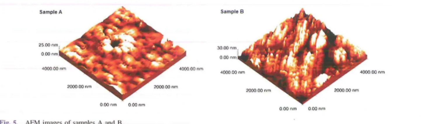
Fig. 5. AFM images of samples A and B.
J. Nanoe/ectron. Optoelectron., 12, 109-117, 2017
3.2. AFM Observations
The difference between the layers of multilayered s
truc-tures is able to cause significant topographic changes on the sample surface. 36 Therefore the surface features of the structures with InGaN layer of samples A and B are
exam-ined by AFM. For this purpose the surface images of the
samples are obtained by using an Omicron YT STM/AFM device. The scans are performed on the surface in an area
of 5 x 5 µ,m2. AFM images obtained by the scans
con-ducted on the InGaN layers of the hetero-structures with
InGaN layer of samples A and B (Fig. 5). It is brought
to attention that there is a difference of the surface
mor-phologies of the samples. Pits are seen on the surfaces of both samples. This is a typical situation for InGaN sur
-faces. However, meanwhile pit array are dominant on the surface of sample A, ordered hillock rows are dominant on the surface of sample B. Furthermore; the two-dimensional growth on the graded sample is more significant compared to the other. This is related to the diffusion of atoms.
On the other hand, roughness is a type of surface imper
-fection. There are many parameters used for the determi-nation of the roughness. Root-mean-square (RMS) is the most widespread parameter used for the evaluation of the surface roughness.36 ·37 The RMS roughness values of sa
m-ples A and B are measured to be 2.24 and 4.88 r espec-tively. These values are determined to be coherent with the smooth surface of sample A, where the lateral growth was greater compared to the others. Chen et al. have reported
segregation of indium next to vacancy islands or ordered vacancy rows on the surface.17·38 According to this, the rough surface of sample B with a higher indium
percent-age attributed to the segregation.
3.3.
JV Analysis
Electrical performanc e of a solar cell could be determined by current density versus voltage (J-V) measurements,
which is the most common technique in photovoltai cs. In value is inversely proportional to Voe in InGaN solar cell structures. Furthermore crystal imperfection in the s truc-tures changes the value of V0c depending on changi ng of
In concentration at low growing temperature.39 The Voe for
the grown InGaN solar cells is typically 0.4 eY. According
30.00nm 0,00nm
0.00 nm 0.00 nm
Microstructural Analysis with Graded and Non-Graded Indium in lnGaN Solar Cell Ourukan el al.
to the V oc value, the solar eel I performances of the graded
sample A and sample B are 3.69% and 2.04%, respec
-tively. In the light of these results, it is determined that the solar efficiency of sample A has a higher performanc e.
These results correspond with the other HRXD , AFM and
JV results. As a result, the continuou s Indium flow indi-cates that the structura l, morphological and electrical fea-tures of sample A are better than that of sample B. Graded InGaN structures have shown an enhanced performance in relaxing the strain in the InGaN/GaN structures grown on sapphire , as compared to conventiona lly grown GaN structur es.40
4. CONCLUSION
In this study, we have studied the graded interlayer s
approach to improve the MOCVD grown InGaN epi-layer quality. By comparing In graded lnGaN structure with non
graded lnGaN structure , we have found that the graded structure can improve the surface morphology and cry
s-talline quality. The graded InGaN layer acts as a "tran -sition layer" between InGaN epilayer and GaN template.
It is demonstrated that the layer can release the strain and can significantly reduce tilt and the dislocations in the InGaN epilayer. Pits on the surfaces of both sam
-ples are seen in the AFM analysis. However , the pit array on the surface of In graded are dominant and the two-dimensional growth is more distinct, compar ed to non graded. In non graded , the ordered hillock rows are domi
-nant. Furthermore , the RMS roughness values of In graded
and non graded are obtained as 2.24 and 4.88 nm, respec-tively. These values show that In graded film is coherent with the smooth surface compared with the non graded one. According to the final conducted JV calculation s the
solar battery performance of the graded samples A and B are determined to be 3.69% and 2.04% respectively. The experimental results show that graded growth of InGaN is a superior growth technique for high performance solar cell devices.
References and Notes
1. J. H. Ryou, W. Lee, J. Limb, D. Yoo, J. P. Liu, R. D. Dupuis,
Z. H. Wu, A. M. Fischer, and F. A. Ponce, Appl. Phys. Lett.
92, 1 (2008).
2. H. Hamzaoui, A. S. Bouazzi, and B. Rezig, Sol. Energ. Mat. Sol. Cells 87, 595 (2005).
3. Q. Deng, X. Wang, H. Xiao, C. Wang, H. Yin, H. Chen, Q. Hou,
D. Lin, J. Li, Z. Wang, and X. Hou, J. Phys. 0, Appl. Phys.
44, 265103 (2011 ).
4. Z. Li, H. Xiao, X. Wang, C. Wang, Q. Deng, L. Jing, J. Ding, Z. Wang, and X. Hou, Chin. Phys. Lett. 30, 068402 (2013).
5. C. H. Chiu, D. W. Lin, Z. Y. Li, S. C. Ling, H. C. Kuo, T. C. Lu,
S. C. Wang, W. T. Liao, T. Tanikawa, Y. Honda, M. Yamaguchi,
and N. Sawaki, Proc. SPIE 7939, 79391 (2011 ).
6. N. C. Das, M. L. Reed, A. V. Sampath, H. Shen, M. Wraback,
R. M. Farrell, M. lza, S. C. Cruz, J. R. Lang, N. G. Young,
Y. Terao, C. J. Neufeld, S. Keller, S. Nakamura, S. P. Denbaars, U. K. Mishra, and J. S. Speck, Journal of Electronic Materials
42 (2013).
116
7. M. Funato, M. Unde, Y. Kawakami, Y. Narukawa, T. Kosugi, M. Takanashi, and T. Mukai, Jpn. J. Appl. Phys. II 45, L659
(2006).
8. T. Lu, C. Kao, H. Kuo, G. Huang, and S. Wang, Appl. Phys.
Lett. 92, 141102 (2008).
9. K. L. Lin, E. Y. Chang, Y. L. Hsiao, W. C. Huang, T. K. Li,
D. Tweet, J. S. Maa, S. T. Hsu, and C. T. Lee, Appl. Phys. Lett. 91, 222111 (2007).
10. A. Krost, A. Dadgar, G. Strassburger, and R. Clos, Phys. Stat. Sol. (a) 200, 26 (2003).
11. Z. Ke-Bao, H. Miao, L. Ping-Yuan, W. Geng, L. Tai-Ping, and D. Chun-Hua, Chinese Physics B 22, 10 (2013).
12. C. E. Kendrick, Revisiting nitride semiconductors, epilayers,
p-type doping and nanowires, Ph.D. Thesis, University of
Canterbury, Canterbury, Christchurch (2008), pp. 63-72.
13. M. G. Suryanarayana, Norton, X-Ray Diffraction: A Practical
Approach, Plenum Press, New York (1998).
14. C. Kisielewski, Semicon. Semimet. 57, 275 (1999).
15. G. Wassermann and J. Grewen, Texturen Metallischer
Werk-stoffe, Springer-Verlag, Berlin, Heidelberg (1962), pp. 754---5.
16. M.A. Moram and M. E. Vickers, Rep. Prog. Phys. 72, 036502
(2009).
17. Y. Ba~. P. Demirel, N. Akin, C. Ba~kose, Y. Ozen, B. K1nac1,
M. K. Ozturk, S. Oz<;;elik, and E. Ozbay, Journal of Materials Science: Materials in Electronics 25, 3924 (2014).
18. M. Schuster, P. 0. Gervais, B. Jobst, W. Hosler, R. Averbeck,
H. Riechert, A. lberlk, and R. Stommerk, J. Phys. 0: Appl.
Phys. 32, 56 (1999).
19. S. I. Cho, K. Chang, and M. S. Kwon, J. Mater. Sci. 43, 406
(2008).
20. C. Kisielewski, J. Kruger, S. Ruvimov, T. Suski, J. W. Ager, E. Jones, Z. Liliental-Weber, M. Rubin, E. R. Weber, M. D.
Bremser, and R. F. Davis, Phys. Rev. B 54, 177 45 (1996).
21. V. Kachkanov, B. Leung, J. Song, Y. Zhang, M.-C. Tsai,
G. Yuan, J. Han2, and K. P. O'Donnell, Scientific Reports
4, 4651 (2014).
22. V. S. Harutyunyan, A. P. Aivazyan, E. R. Weber, Y. Kim, Y. Park, and S. G. Subramanya, J. Phys. 0: Appl. Phys. 34, A35 (2001). 23. G. K. Williamson and W. H. Hall, Acta Metal/. 1, 22 (1953).
24. Md. Rafiqul Islam, Y. Ohmura, A. Hashimoto, A. Yamamoto,
K. Kinoshita, and Y. Koji, Phys. Status Solidi C 7, 2097 (2010).
25. Md. Rafiqul Islam and Md. Arafat Hossain, IEEEIOSAI/APR
International Conference on lnfonnatics, Electronics and
Vision, IC/EV, Dhaka, Bangladesh (2012).
26. A. Hossain, R. Islam, M. K. Hossain, A. Hashimoto, and
A. Yamamoto, Mater. Renew. Sustain Energy 10, 2 (2014).
27. 0. Ambacher, Journal of Applied 31, 2653 (1998).
28. E. Arslan, M. K. Ozturk, 0. Duygulu, A. A. Kaya, S. Oz<;;elik,
and E. Ozbay, Applied Physics A-Materials Science and Pro-cessing 94, 73 (2009).
29. N. G. Weimann, L. F. Eastman, 0. Doppalapudi, M. N. Hock, and T. D. Moustakas, J. Appl. Phys. 83, 3656 (1998).
30. M. E. Vickers, M. J. Kappers, R. Datta, C. McAleese, T. M.
Smeeton, F. D. G. Rayment, and C. J. Humphreys, J. Phys. D:
Appl. Phys. 38, A99 (2005).
31. X. H. Zheng, H. Chen, Z. B. Yan, Y. J. Han, H. B. Yu, D. S. Li,
Q. Huang, and J. M. Zhou, J. Cryst. Growth 255, 63 (2003). 32. S. C. Jain, M. Willander, J. Narayan, and R. V. Overstraeten,
J. Appl. Phys. 87, 965 (2000).
33. 0. Brandt, Y. J. Sun, H. P. Schbnherr, K. H. Ploog, P. Wal
-tereit, S. H. Lim, and J. S. Speck, Appl. Phys. Lett. 83, 90
(2003).
34. J. K. Sheu, IEEE Electron Device Letters 30, 225
(2009).
0urukan et al. Microstructural Analysis with Graded and Non-Graded Indium in lnGaN Solar Cell
35. P. Gay, P. B. Hirsch, and A. Kelly, Acta Metal/. 1, 315 (1953).
36. S. <;orekr;;i, M.K. Ozturk, M. <;akmak, S. bzr;;elik, and E. Ozbay, Mater. Sci. Semicond. Process. 15, 32 (2012).
37. S. <;orekci, M. K. Ozturk, A. Bengi, M. <;akmak, S. bzr;;elik, and E. Ozbay, J. Mater. Sci. 46, 1606 (2011 ).
38. T. Tao, Z. Zhao, L. Lian, S. Hui, X. Zili, Z. Rong, L. Bin,
X. Xiangqian, L. Yi, H. Ping, S. Yi, and Z. Youdou, Journal of Semiconductors 32, 1 (2011 ).
J. Nanoelectron. Optoelectron., 12, 109-117, 2017
39. 0. Jani, P. Mahala, S. K. Behura, A. Ray, and C. Dhanavantri,
The effect of indium composition on open-circuit voltage of
lnGaN thin-film solar cell: An analytical and computer simul
a-tion study, A/P Conf Proc., Mumbai, India (2012), Vol. 1451. 40. T. L. Song, S. J. Chua, and E. A. Fitzgerald, Graded lnGaN
Buffers for Strain Relaxation in GaN/lnGaN Epliayers Grown on Sapphire, OSpace@MIT: Massachusetts Institute of Tec h-nology (2002).