A Novel Grounded Inductor Realization Using a
In this study, we present a new topology for realizing a grounded inductor employing only a single current conveyor, called a negative-type modified inverting second-generation current conveyor (MICCII-), and a minimum number of passive components, two resistors, and one capacitor. The non-ideality effects of the MICCII- on a simulated inductor are investigated. To demonstrate the performance of the presented inductance simulator, we use it to construct a third order Butterworth high-pass filter and a parallel resonant circuit. Simulation results are given to confirm the theoretical analysis.
Keywords: Grounded inductance simulator, current conveyor, high-pass filter.
Manuscript received Oct. 24, 2004; revised Mar. 8, 2005.
Erkan Yuce (phone: + 90 212 359 73 97, email: [email protected]) and Oguzhan Cicekoglu (email: [email protected]) are with the Department of Electrical and Electronic Engineering, Bogazici University, Turkey.
Shahram Minaei (email: [email protected]) is with the Department of Electronics and Communication Engineering, Dogus University, Turkey.
I. Introduction
Minimum Number of Active and Passive Components
Erkan Yuce, Shahram Minaei, and Oguzhan Cicekoglu
Monolithic Si spiral inductors suffer from substrate resistive losses and capacitive couplings. In addition, process tolerances lead to component variations, which cannot easily be tuned in the passive case [1]. Thus active circuits, which simulate the characteristic of a passive inductor, have received considerable attention. This is attributed to their effective use of space, weight, cost, tunability, integrability, and the wide range of applications of such inductors especially when the value of the required inductance is relatively large. The most famous inductance simulator was proposed by Antoniou [2] and utilizes two op-amps and five passive elements to obtain a pure inductance. However, as an active element, a current conveyor (CC) provides many advantages such as greater linearity, wider bandwidth, and better dynamic range compared to the voltage mode counterparts, op-amps [3].
Many CC-based grounded synthetic inductor topologies have been proposed in the literature [4]-[15]. These topologies can be classified based on the number of active and passive elements employed and whether they realize a lossy or lossless kind of inductor. Most of these circuits employ two or more CCs to realize grounded inductance [6]-[8], [10]-[12], and [15]. The proposed topologies in [4], [9], [13], and [14] employ a single CC but they do not realize pure inductance. Although the circuit reported in [5] realizes pure inductance with only one positive type second-generation current conveyor (CCII+), it employs five passive elements.
On the other hand, new types of CCs such as the inverting second-generation current conveyor (ICCII) [16] have been proposed in the literature. Such kinds of current conveyors give a higher degree of freedom to analog designers, with respect to op-amp and CCII solutions, allowing the implementation of
more functions using less active elements. A circuit with a minimum number of components is expected to simplify the design.
In this paper, we propose a grounded inductance simulator employing a minimum number of active and passive components including one modified inverting second-generation current conveyor (MICCII), two resistors, and one capacitor. The proposed topology ideally provides lossless inductor realization. By taking non-idealities of the MICCII (due to current and voltage gain) into account, several kinds of grounded immitances can be obtained. Finally, using the proposed grounded inductance simulator, a third-order Butterworth high-pass ladder filter and a parallel resonant circuit is constructed. Frequency domain and time domain responses are given to illustrate the performance of the proposed circuit.
II. Proposed Circuit
A symbolic representation of the MICCII is shown in Fig.1. The MICCII can be characterized by the following matrix equation ⎥ ⎥ ⎥ ⎦ ⎤ ⎢ ⎢ ⎢ ⎣ ⎡ ⎥ ⎥ ⎥ ⎦ ⎤ ⎢ ⎢ ⎢ ⎣ ⎡ ± − = ⎥ ⎥ ⎥ ⎦ ⎤ ⎢ ⎢ ⎢ ⎣ ⎡ z x y z y x V I V I I V 0 2 0 0 0 0 0 0 α β , (1)
where α and β represent the non-ideal current and voltage gains of the current conveyor (ideally equal to unity), respectively.
Fig. 1. Symbol of the MICCII-. Vy Vx Iy Ix Iz Vz Y X MICCII- Z
Conventionally, the + or - signs of α in (1) denote the positive (MICCII+) and negative (MICCII−) type conveyors.
The proposed grounded inductor is shown in Fig. 2. It uses one MICCII− and three passive elements. To find the input admittance of the circuit, a voltage source Vin is connected to
the X-terminal of the current conveyor of the proposed circuit. For the Y, X and Z terminals of the MICCII−, we can write
3 2 (V V )y y Vy = z− y , (2a) x z x in V V y I I =( − ) 1+ , (2b) and 3 1 ( ) ) (V V y V V y Iz= z− x + z− y − , (2c)
respectively. Using the terminal characteristic equation of the MICCII- given in (1) and (2a) through (2c), we can obtain the following admittance: 2 2 2 1 3 2 1 y y y y y V I Y in in in= = + − . (3)
If y1=G, y2=2G, and y3=sC in (3) are chosen, the following
impedance is obtained: 2 1 G sC sL Y Z eq in in = = = . (4) Hence, 2 G C Leq= . (5)
Thus, a lossless grounded inductor is realized using a minimum number of passive and active components.
Fig. 2. The proposed inductor realization using MICCII- and passive components. MICCII- y2 y3 Zin Vin Iin y1 X Y Z
III. Non-ideality Effects
Taking into account the non-idealities given in (1), the equivalent non-ideal impedance of the circuit is found to be
) 3 2 2 ( ) 1 2 ( 2 2 2 − + + − − = β αβ α α αβ sCG G sC Zin . (6)
From (6), the admittance of the circuit is calculated as αβ β αβ α αβ α 2 ) 3 2 2 ( ) 1 2 ( 1 1 2 + − − + − = + = G sC G R sL Y p p in . (7)
Therefore, the circuit simulates an inductor in parallel with a resistor calculated as ⎪ ⎪ ⎭ ⎪ ⎪ ⎬ ⎫ − − + = − = ) 3 2 2 ( 2 ) 1 2 ( 2 β αβ α αβ α αβ G R G C L p p . (8)
In this case, the quality factor of the inductor is found to be
) 3 2 2 ( ) 1 2 ( 2 − − + − = = β αβ α ω α ω C G L R Q p p L . (9)
Note that one can change the α parameter of MICCII- by adjusting bias voltages of the MICCII-, so considering β=1 and α as a variable, five types of inductors can be obtained:
a) For α>1, a lossless inductor in parallel with a positive resistance is obtained.
b) For α = 1, a pure (lossless) inductor as described in section II is realized.
c) For 0.5<α<1, a lossless inductor in parallel with a negative resistor is obtained.
d) For 0<α<0.5, a negative inductor in parallel with a negative resistor is obtained.
e) For α <0, a lossless inductor in parallel with a positive resistor is obtained. In this case, the MICCII- is converted to a MICCII+.
IV. Simulations
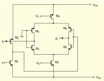
The MICCII- is constructed using the schematic implementation in Fig. 3 with DC supply voltages equal to ±2.5 V and bias voltages equal to VB=– 0.604 V and VC=– 0.25
V. The simulations are performed using SPICE based on 0.35 µm Taiwan Semiconductor Manufacturing Company, Ltd. (TSMC) CMOS technology tabulated in Table 1. The dimensions of the MOS transistors used in the MICCII- implementation are given in Table 2. To investigate what is the frequency range for the designed MICCII-, AC simulations have been performed. The Iz/Ix and Vx/Vy frequency responses
of the MICCII- are depicted in Fig. 4. The α and β values of the MICCII- are found to be 1.02 and 0.967, respectively. The frequency behavior reported in Fig. 4 suggests that for high
Fig. 3. The internal structure of the MICCII-. M8 M7 VB VC Z- M2 M1 VSS VDD Y X M3 M5 M4 M6
Table 1. Parameters of the CMOS transistors used in SPICE simulations.
0.35µm TSMC CMOS parameters .MODEL CMOSN NMOS ( LEVEL = 3
+ TOX = 7.9E-9 NSUB = 1E17 GAMMA = 0.5827871 + PHI = 0.7 VTO = 0.5445549 DELTA = 0
+ UO = 436.256147 ETA = 0 THETA = 0.1749684
+ KN = 2.055786E-4 VMAX = 8.309444E4 KAPPA = 0.2574081 + RSH = 0.0559398 NFS = 1E12 TPG = 1
+ XJ = 3E-7 LD = 3.162278E-11 WD = 7.046724E-8 + CGDO = 2.82E-10 CGSO = 2.82E-10 CGBO = 1E-10 + CJ = 1E-3 PB = 0.9758533 MJ = 0.3448504
+ CJSW = 3.777852E-10 MJSW = 0.3508721 ) .MODEL CMOSP PMOS ( LEVEL = 3
+ TOX = 7.9E-9 NSUB = 1E17 GAMMA = 0.4083894
+ PHI = 0.7 VTO = –0.7140674 DELTA = 0
+ UO = 212.2319801 ETA = 9.999762E-4 THETA = 0.2020774 + KP = 6.733755E-5 VMAX = 1.181551E5 KAPPA = 1.5
+ RSH = 30.0712458 NFS = 1E12 TPG = –1
+ XJ = 2E-7 LD = 5.000001E-13 WD = 1.249872E-7 + CGDO = 3.09E-10 CGSO = 3.09E-10 CGBO = 1E-10 + CJ = 1.419508E-3 PB = 0.8152753 MJ = 0.5 + CJSW = 4.813504E-10 MJSW = 0.5 )
frequency applications (frequencies of more than 77 MHz), a compensation is needed.
The proposed circuit shown in Fig. 2 is simulated with the following passive element values: G = 1 mS (y1=G1=1 mS and
y2=G2=2 mS) and C = 50 pF, which results in Leq= 50 µH. The
power consumption of the designed grounded inductor is found to be 17.6 mW.
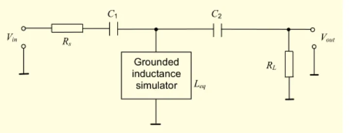
To evaluate the performance of the proposed inductance simulator, we use it in the structure of a third-order Butterworth high-pass ladder filter shown in Fig. 5. The passive elements
Table 2. Dimensions of the CMOS transistors. PMOS transistors W(µm)/L(µm) M2 28/28 M5 24.85/0.35 M6 19.6/0.35 M8 57.75/1.05 NMOS transistors W(µm)/L(µm) M1 8.75/28 M3 9.8/0.35 M4 9.8/0.35 M7 27.65/1.05
Fig. 4. The simulated frequency responses of the Iz/Ix and Vx/Vy
for the MICCII-.
1 Hz 100 Hz 10 kHz 1 MHz 100 MHz 10 GHz Frequency -40 -30 -20 -10 0 10 20 30 40 Gain (dB ) Iz/Ix Vx/Vy
Fig. 5. Third-order high-pass ladder filter prototype.
C1 C2 Leq RL Vout Rs Vin Grounded inductance simulator
are selected as C1=C2=0.1 nF, RL=Rs=1 kΩ, and synthetic
inductor Leq = 50 µH, which results in a 3 dB frequency of
1.59 MHz. Both ideal and simulated high-pass ladder filter responses are shown in Fig. 6.
To exhibit the time domain performance of the proposed simulated inductor, a triangular input current with a 0.5 mA peak is applied to the proposed inductor (Leq=175 µH, obtained
by G = 1 mS and C = 175 pF) to obtain a square wave output voltage, as shown in Fig. 7.
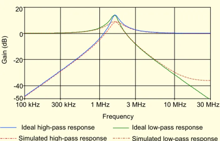
Also, the proposed grounded inductance is used to construct a parallel resonant circuit as shown in Fig. 8. The element values are selected as Leq=LP=100 µH (G = 1 mS and
Fig. 6. The ideal and simulated frequency responses of the third-order Butterworth high-pass ladder filter.
Frequency 10 kHZ 30 kHz 100 kHz 300 kHz 1 MHz 3 MHz 10 MHz 30 MHz 100 MHz -150 -100 -50 0 Gain (dB ) Simulated response Ideal response
Fig. 7.The ideal and simulated time domain responses of the proposed inductor. Time (µs) 4 8 12 16 20 -50 0 50 -1 0 Iin (mA )
Triangular input current Ideal response Simulated response 1
Vout
(mV
)
Fig. 8. Parallel resonant circuit. Grounded inductance simulator LP Ihp C1 R1 Ibp Ilp Iin
C = 100 pF), C1=0.1 nF, and R1=5 kΩ. Ideal and simulated
high-pass (Ihp) and low-pass (Ilp) responses of the parallel
resonant circuit are given in Fig. 9. Moreover, both ideal and simulated band-pass (Ibp) responses are depicted in Fig. 10.
From Fig. 10, we can see that a gain error exists at the resonance frequency, which is due to the parallel resistance (Rp)
of the simulated inductance. Considering α =1.02 and β =0.967 for the designed MICCII-, from (8) and (9), one can calculate the simulated inductance and its parallel resistance as
Lp = 94.8 µH and Rp = 43.18 kΩ, respectively. Therefore, the
quality factor of the simulated inductance at a frequency of 1.59 MHz is found to be QL = 45.5.
Fig. 9. Ideal and simulated high-pass and low-pass responses of the circuit in Fig. 8.
Frequency 100 kHz 300 kHz 1 MHz 3 MHz 10 MHz 30 MHz -40 -20 0 20 -50 Ga in (d B )
Ideal high-pass response Simulated high-pass response
Ideal low-pass response Simulated low-pass response
Fig. 10. Ideal and simulated band-pass responses of the circuit shown in Fig. 8. Frequency 100 kHz -40 300 kHz 1 MHz 3 MHz 10 MHz 30 MHz -30 -20 -10 0 Gain (dB )
Ideal response Simulated response
From Figs. 6, 7, 9 and 10, we can see that the simulation results agree well with the theory.
V. Conclusion
In this paper, we presented a grounded inductor simulating topology. The proposed topology allows for a design with a minimum number of active and passive components, such as two resistors and one capacitor, and one MICCII-. We also investigated the non-ideality effects of the MICCII- on the proposed inductor. To demonstrate the frequency and time-domain behavior of the proposed inductor, we performed simulations with SPICE using 0.35 µm TSMC CMOS technology. The simulation results verify the theoretical analysis.
References
[1] G. Thanachayanont and A. Payne, “CMOS Floating Active
Inductor and its Applications to Bandpass Filter and Oscillator Designs,” IEE Proc.-Circuits Devices Syst., vol. 147, 2000, pp. 42-48.
[2] A. Antoniou, “Realization of Gyrators Using Operational Amplifiers, and their Use in RC-Active-Network Synthesis,” Proc. of the IEE, vol. 116, 1969, pp. 1838-1850.
[3] G. Ferri and N.C. Guerrini, “Low-Voltage Low-Power CMOS Current Conveyors,” Kluwer Academic Publishers, London, 2003. [4] R. Senani, “Active Simulation of Inductors Using Current
Conveyors,” Electronics Lett., vol. 14, 1978, pp. 483-484. [5] A.N. Paul and D. Patranabis, “Active Simulation of Grounded
Inductors Using a Single Current Conveyor,” IEEE Trans. on Circuits and Systems, vol. 28, 1981, pp. 164-165.
[6] W. Surakampontorn and P. Thitimajshima, “Integrable Electronically Tunable Current Conveyors,” IEE Proc., Pt. G, vol. 135, 1988, pp. 71-77.
[7] I.A. Khan, M.T. Ahmed, and N. Minhaj, “Novel Technique for Immitance Simulation–Realisation of Some All-Active Simulators,” Int’l J. of Electronics, vol. 72, 1992, pp. 431-441. [8] C.L. Hou, R.D. Chen, Y.P. Wu, and P.C. Hu, “Realization of
Grounded and Floating Immitance Function Simulators Using Current Conveyors,” Int’l J. of Electronics, vol. 74, 1993, pp. 917-923.
[9] C.M. Chang, H.Y. Wang, and C.C. Chien, “Realization of Series Impedance Functions Using one CCII+,” Int’l J. of Electronics, vol. 76, 1994, pp. 83-85.
[10] S.I. Liu and C.Y. Yang “Higher-Order Immitance Function Synthesis Using CCIIIs,” Electronics Lett., vol. 32, 1996, pp. 2295-2296.
[11] A. Fabre, H. Amrani, and O. Saaid, “Current-Mode Bandpass Filters with Q Magnification,” IEEE Trans. on Circuits and Systems-II, vol. 43, 1996, pp. 839-842.
[12] O. Çiçekoğlu, “Active Simulation of Grounded Inductors with CCII+s and Grounded Passive Elements,” Int’l J. of Electronics, vol. 85, 1998, pp. 455-462.
[13] H. Kuntman, M. Gülsoy, and O. Çiçekoğlu, “Actively Simulated Grounded Lossy Inductors Using Third Generation Current Conveyors,” Microelectronics J., vol. 31, 2000, pp. 245-250. [14] H.Y. Wang and C.T. Lee, “Systematic Synthesis of R-L and C-D
Immitances Using CCIII, Int’l J. of Electronics, vol. 87, 2000, pp. 293-301.
[15] G. Ferri and N. Guerrini, “High-Valued Passive Element Simulation Using Low-Voltage Low-Power Current Conveyors for Fully Integrated Applications,” IEEE Trans. on Circuits and Systems-II, vol. 48, 2001, pp. 405-409.
[16] I.A. Awad and A.M. Soliman, “Inverting Second Generation Current Conveyors: the Missing Building Blocks, CMOS Realizations and Applications,” Int’l J. of Electronics, vol. 86, 1999, pp. 413-432.
Erkan Yuce was born in 1969 in Nigde, Turkey. He received the BS degree from Middle East Technical University and MS degree from Pamukkale University in 1994 and 1998. He is currently a PhD student in electrical and electronics engineering at Bogazici University. He is currently a research assistant at the Electrical and Electronics Engineering Department of Bogazici University. His current research interests include analog circuits, active filters, synthetic inductors, and current-mode circuits. He is the author or co-author of about 10 papers published in scientific journals or conference proceedings.
Shahram Minaei received the BS degree in electrical and electronics engineering from Iran University of Science and Technology in 1993. He received the MS and PhD degrees in electronics and communication engineering from Istanbul Technical University in 1997 and 2001. He is currently an Associate Professor at the Electronics and Communication Engineering Department of Dogus University in Istanbul, Turkey. He has more than 50 journal or conference papers in scientific review. He served as a reviewer for a number of international journals and conferences. His current field of research concerns current-mode circuits and analog signal processing. He is a member of IEEE.
Oguzhan Cicekoglu was born in 1963 in Istanbul, Turkey. He received the BS and MS degrees from Bogazici University and the PhD degree from Istanbul Technical University all in electrical and electronics engineering in 1985, 1988 and 1996. He served as a lecturer at the School of Advanced Vocational Studies Electronics Prog. of Bogazici University, where he held various administrative positions between 1993 and 1999, and as part time lecturer at various institutions. He was with Biomedical Engineering Institute between 1999 and 2001. He is currently an Associate Professor at the Electrical and Electronics Engineering Department of Bogazici University. His current research interests include analog circuits, active filters, analog signal processing applications and current-mode circuits. He is the author or co-author of about 150 papers published in scientific journals or conference proceedings. He is a member of IEEE.