Carbon string structures: First-principles calculations of quantum conductance
R. T. Senger, S. Tongay, S. Dag, E. Durgun, and S. Ciraci*Department of Physics, Bilkent University, 06800 Ankara, Turkey
共Received 24 August 2004; revised manuscript received 10 February 2005; published 9 June 2005兲
Carbon forms various nanostructures based on the monatomic chains or strings which show transport properties of fundamental and technological interest. We have carried out first-principles quantum conductance calculations using optimized structures within density functional theory. We treated finite segments of carbon monatomic chain, metal-semiconductor heterostructure, and resonant tunneling double barrier formed of C-BN chains, as well as symmetric and antisymmetric loop devices between two electrodes. We examined the effects of electrode, contact geometry, size of the device, strain, and foreign atoms adsorbed on the chain. Calculated quantum ballistic conductance of carbon chains showing even-odd disparity depending on the number of atoms and strain are of particular interest. Notably, chains consisting of an even number of carbon atoms contacted to metal electrodes display a resonant tunneling-like behavior under axial strain. The double covalent bonding of carbon atoms depicted through self-consistent charge density analysis underlies unusual transport properties. DOI: 10.1103/PhysRevB.71.235406 PACS number共s兲: 73.63.⫺b, 73.22.⫺f, 73.40.Jn
I. INTRODUCTION
As the research on molecular electronics 共or moletronics兲1,2has been in progress for several decades, con-necting those nanodevices has remained a real challenge. In an effort to develop highly conducting interconnects, intense research has focused on nanowires,3which revealed unusual
mechanical and transport properties of metallic wires.4–7 In
particular, a close correlation between their atomic structure and stepwise variation of conductance has attracted interest.8–10 Following predictions of several theoretical
studies11–13 the production of monatomic linear gold chain
has been a breakthrough.14,15 More recently, multiwall and
single-wall tubular wires of gold have been observed and studied.16–18 While those thin metal wires drawn between
two electrodes have been useful to reveal fundamental as-pects of quantum ballistic conductance, they were not repro-ducible, and hence were unsuitable for device applications. Carbon nanotubes19,20 with their unusual mechanical and
electronic properties have been considered as a promising class of nanostructures meeting several requirements and of-fering new paradigms in nanoelectronics. Further to several device applications, single-wall carbon nanotubes 共SWNT兲 are also considered as interconnects. Experimentally and theoretically it has been shown that SWNTs can be uni-formly coated with Ti atoms.21,22With their high
conductiv-ity and polarized spins at the Fermi level, coated carbon nanotubes appear to be suitable for spintronic applications.22
Another ultimate one-dimensional 共1D兲 nanowire, namely, monatomic linear chain of carbon atoms 共C-LC兲, attracted the interest of several researchers much earlier.23–29 Using chemical methods, production of carbon monatomic chains up to 20 atoms in length has been achieved.30
Re-cently, C-LC has been observed at the center of multiwall carbon nanotubes.31
The transport properties of C-LC have attracted consider-able attention owing to its ultimate size in fabricating nanodevices. Lang and Avouris32 studied the conductance
variation of finite-size C-LCs having N atoms共3艋N艋7兲 in contact with two jellium electrodes. They found that the
equilibrium conductance G共N兲 varies in an oscillatory man-ner, with odd-numbered C-LCs having a higher conductance than even-numbered ones. This oscillatory variation of con-ductance was attributed to the effect of N on the occupation of the degenerate⑀共x兲=⑀共y兲 levels and their modification by the coupling of jellium electrodes. The combined effect is reflected in the state density at the Fermi level of the electrode-C-LC-electrode system. The oscillatory behavior of G共N兲 was revealed earlier also for the Na-chain structure.33Similar arguments based on the Laughlin
Kalm-eyer theory34 were used in explaining the conductance
through a single Al atom between two metal electrodes.35
Later, Lang and Avouris36showed that there is a large
trans-fer of charge from the electrodes to the chain, which pro-vides doping of the chain without introducing scattering cen-ters. Recently, Larade et al.37 reported a first-principles
analysis of finite-size C-LCs with 4艋N艋7 in contact with two crystalline Al-electrodes under external bias. Their work demonstrated that the conductance is affected by the crystal-line order of electrodes, and coupling between carbon chain and Al electrodes is one of the major factors controlling the transport. Accordingly, whether carbon atoms were attached to the top site or hollow site on the Al electrode becomes significant as pointed out much earlier.35 Most importantly,
the even-odd disparity in the number of chain atoms found by Larade et al.37 has a trend opposite to that obtained in jellium-electrode calculations, even-numbered chains having higher conductance values than odd-numbered ones. The first-principles analysis has also revealed a negative differen-tial resistance at finite biases owing to a shift of conduction channels relative to the states of Al electrodes.37
This paper presents an extensive study of the transport properties of various structures based on carbon strings using first-principles calculations of quantum conductance. Our preliminary results have been reported as a short letter.38
Here we extend our analysis to investigate the effect of elec-trodes, contact geometry, strain, and device-size which shows interesting even-odd disparity in the number of atoms. We also examined atomic string heterostructures and loop devices.
density functional theory 共DFT兲. All infinite and finite-size nanostructures in our study have been treated within super-cell geometries. Generalized gradient approximation42
共GGA兲 and local density approximation43 共LDA兲 have been
used in the calculations. The reported values are GGA results unless otherwise stated. All the atomic positions and lattice parameters of periodic structures have been optimized by minimizing the total energy, forces on atoms, and the stress on the structure. For the ultrasoft pseudopotentials40,44used
in our calculations the wave functions are represented by plane waves up to kinetic energy cutoff 兩k+G兩⬵400 eV. The Brillouin zones of various structures have been sampled by the Monkhorst-Pack k-point sampling scheme.45 The
number of k-points are determined by performing conver-gence tests, which yield 1⫻1⫻51 mesh appropriate for the case of C-LC with a single atom per supercell. For larger supercells, the appropriate numbers of k-points have been set by scaling according to the size of the unit cell.
The analysis of quantum ballistic conductance for infinite and finite size structures have been performed using TRANSIESTA-C, a recently developed ab initio transport software based on DFT, localized basis sets, and nonequilib-rium Green’s function 共NEGF兲 formalism.46,47 In
TRANSIESTA-C we have employed double-zeta-parameter numerical basis sets which are usually comparable to well converged plane wave basis sets. As usual, we have used an electrode-device-electrode geometry for conductance calcu-lations. The conductance of the device has been calculated as
G共E兲 =2e
2
h Tr共⌫lG r⌫
rGa兲 共1兲
after iteratively solving nonequilibrium Green’s function and DFT equations.47 In the above equation, Gr and Ga are re-tarded and advanced Green’s functions, and ⌫l and ⌫r are coupling functions to the left and right electrodes, respec-tively. In order to match the device potential and the surface potential of the semi-infinite electrodes, the device regions are defined to contain some portions of the electrodes.
DFT is employed to describe exchange correlation and charging effects as well as the atomic structure of both the device and the electrodes in a self-consistent manner. Unlike conventional DFT simulation schemes, in order to account for the infinite and open nature of the system due to the electrodes, DFT is used in combination with NEGF formal-ism. The latter provides the means for representing the ef-fects of infinite electrodes in the form of self-energy terms.
III. RESULTS AND DISCUSSION
Earlier, we treated the conductance of periodic, infinite C-LC, infinite and finite helix structures CuHX共N,p兲in Ref. 38, where the mechanical and electronic structure of carbon monatomic strings are also discussed to some extent. Unlike
most other elements and compounds, monatomic strings of carbon do not tend to form zigzag chains. The carbon atomic chain is stiff along its axis but flexible in the transverse directions.38 In Fig. 1 the total energy and tension variations
in periodic C-LC as functions of the lattice parameter are shown. The equilibrium lattice constant is 1.27 Å. As the chain is stretched homogenously both the energy and the tension of the chain increase. At the point where the maxi-mum value of the tension is reached, the velocity of sound of the longitudinal-acoustic mode is zero, and the chain breaks due to long-wavelength perturbations.48 For C-LC the slope
of the tension becomes zero at c = 1.56 Å, which corresponds to a maximum strain value of ⑀= 0.23 before the chain breaks.
In the present work we are concerned with the conduc-tance of the unstrained and strained finite segment of C-LC between different types of electrodes, the finite segment of C-LC having substitutional impurity, 共BN兲3 barrier, 共BN兲3C6共BN兲3resonant tunneling double barrier, and
asym-metric and symasym-metric loop devices. We will address impor-tant questions, which have not been investigated thoroughly yet and reveal the effect of size, axial strain, geometry, and also the type of electrodes on the transport properties.
In atomic scales, the detailed atomic structure of contact and the type of the electrodes have considerable effects on the conductance of the molecular conductors. We first choose to use C-LC as the metallic electrodes. The atoms in the device region are subjected to geometry optimizations in su-percells, keeping the electrode-atom positions fixed. The ge-ometry optimization has been performed also for devices un-der axial strain. Accordingly, interatomic distances in the device and the distance between the electrodes and the chain are determined by minimization of the total energy. We also FIG. 1. Total energy per atom and tension of carbon linear chain as functions of lattice parameter. The energies are given relative to the energy of the isolated C atom. The energy curve is a best fit to the calculated values共circles兲, then the tension curve is obtained by differentiation. The vertical dashed line separates the stable and unstable domains of the chain with respect to a longitudinal deformation.
used Al electrodes having a specific crystalline orientation to reveal the effect of the electrodes on conductance properties.
A. Conductance of carbon chain segments
First, we consider the conductance of a C-LC segment under applied strain. Here the C-LC segment having N car-bon atoms is in contact with two electrodes taken as also semi-infinite C-LCs. By using C-LC electrodes we intend to achieve perfect contacts to the chain. Here, while semi-infinite C-LCs are kept in their ideal atomic configuration, the N-atom segment of the chain in the device region is strained. When an axial tension F is applied to an N-atom chain, the length L of the chain increases so that L→L共1 +⑀兲. We optimize the atomic positions of the elongated seg-ment by keeping the separation of two C-LC electrodes at
L共1+⑀兲. The strain leads to nonuniform bond lengths in the
device region. For example, in a six-atom C-LC under a strain of ⑀= 0.15 the sequence of equilibrium bond lengths becomes 1.56,1.31,1.59,1.30,1.59,1.31,1.56 Å after relax-ation. The lengths of the bonds between the terminal atoms of the chain and the electrodes are equal to 1.56 Å. The resulting conductance spectrum of these strained chains dis-plays oscillatory behavior with E. Figure 2 presents G共E兲 of a finite C-LC device containing N = 4 – 7 atoms subjected a strain of⑀= 0.15. The character of oscillations is dramatically different depending on N being odd or even. If N is odd, the chain always has a peak conductance value of 2G0 at the Fermi level, whereas for even N, G共EF兲 corresponds to a minimum of oscillations which drops considerably with in-creasing⑀. This salient feature is related to the alignment of the molecular energy levels of the device region with the electrochemical potential of the electrodes. It turns out that
EFcoincides with the HOMO for odd-numbered chains, and with the center of the HOMO-LUMO gap for
even-numbered ones. When geometrical optimization of the chain is omitted and the strain is assumed to be uniform the con-ductance oscillations are still present but their amplitudes are smaller.38The observation that even-numbered, strained car-bon chains have lower conductance values is compatible with the findings of Lang and Avouris for unstrained chains.32 They reported G⯝1.8G
0 for carbon chains with
N = 5 and 7 in between jellium metal electrodes. In our
model, the use of C-LC electrodes naturally corresponds to a better or even perfect contact that leads to G = 2G0. With our
choice of electrodes, unlike the results in Ref. 32, the differ-ence of N being odd or even in the calculated conductance of unstrained 共⑀= 0兲 carbon chain does not manifest itself, be-cause for all N the configuration is the same. Therefore the odd-even N disparity we find in the conductance of carbon chains is a pure strain-induced effect.
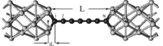
To study the effect of electrodes on the strain-free and strained carbon chains we also consider another system where a finite size共or a segment of兲 C-LC is in contact with two metal electrodes. As metal electrodes, we consider Al bars consisting of 共001兲 planes, where 关001兴 crystalline di-rection is taken parallel to the chain axis. The atomic posi-tions of atoms in the Al electrodes have been optimized in the infinite wire configuration. Once the N-atom chains are connected to the hollow sites of the Al electrodes, the atomic positions of C atoms are optimized by minimizing the total energy and stress while keeping the distance L between the two Al electrodes fixed. In that optimization step, C atoms are allowed to move but Al electrodes are assumed to be rigid. It should be pointed out that the assumption of rigid electrodes is an approximation, in particular for strained sys-tems. However, we consider these as model systems and our emphasis is on the response of carbon atomic chains to ex-ternal strains. In principle, the part of the electrodes in the device region should also be allowed to relax, but deforma-tions in the electrodes would prohibit one to attribute the conductance modifications to the carbon chain alone. In our electrode-device-electrode configuration, each device is a segment of C-LC consisting of N atoms 共N=4,5,6,7兲 as shown in Fig. 3. It is similar to the model considered in Ref. 37, except that in the present case chain-electrode distances,
de, and all CuC bond lengths are optimized.
The optimized 共equilibrium兲 carbon positions at zero strain exhibit interesting features worth emphasizing: First, the CuC bond lengths are not uniform. For N=4, de = 0.84 Å共or dAluC= 2.2 Å兲; and the sequence of equilibrium
FIG. 2. Variation of calculated conductance G共E兲 of a segment of strained C-LC placed between two semi-infinite, strain-free car-bon linear chains as electrodes. Fermi levels are set to zero. Atomic positions in the segments consisting of N = 4,5,6,7 atoms are opti-mized for the value of strain⑀=0.15 and resulted in nonuniform CuC bond distances.
FIG. 3. The electrode-device-electrode model used for the cal-culation of conductance of finite C-LC consisting of N = 4 , 5 , 6 , 7 atoms. Electrodes are taken as Al共001兲 bars made by consecutive squares and centered squares 共rotated by 45°兲 representing 共001兲 planes of an Al fcc crystal perpendicular to the chain axis. L is the spacing between two electrode surfaces, deis the distance between the electrode surfaces and the terminal atoms of the C-LC segment.
CuC bond lengths starting from the first carbon atom in Fig. 3 are 1.34, 1.25, and 1.34 Å. Whereas for N = 5, de = 0.92 Å共or dAluC= 2.3 Å兲; and the sequence of four
equi-librium CuC bond lengths is 1.34, 1.26, 1.26, and 1.34 Å. Considering N = 6 and 7, the equilibrium distance from the end atom of the chain to the last atomic plane of electrode changes in the range 0.84艋de艋0.95 Å; as for the CuC bond lengths, they are nonuniform with specific symmetry and vary in the range 1.25艋di,i+1艋1.34 Å.
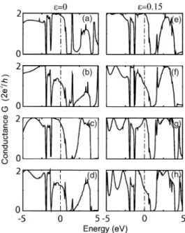
The variation of calculated equilibrium conductance of the system described in Fig. 3 with a finite segment of C-LC comprising a different number of atoms 共N=4–7兲 under ⑀ = 0 is shown in Figs. 4共a兲–4共d兲 in the energy range −5 eV
艋E艋5 eV. The conductance spectrum is derived from the
electronic structure of two electrodes coupled to the
N-carbon atom chain for Al electrodes. The electronic energy
level structure of the chain strongly depends on N and CuC bond lengths, di,i+1, and it shifts and broadens depending on the strength of coupling with metal electrodes. Eventually, the resulting transmission coefficient and G共E兲 incorporate all these effects self-consistently.
Figure 5 shows the dependence of the equilibrium con-ductance values on the number of carbon atoms present in the chain 共zero strain兲. The value of G共E=EF兲 varies be-tween⬃1.8 and 1.2 G0 for optimized C-LC segments with
Al electrodes and under⑀= 0. As far as the even-odd dispar-ity is concerned, the trend depicted in Fig. 5 agrees with the trend reported by Larade et al.,37 but disagrees with the
variation obtained from jellium calculations by Lang and Avouris.32
In order to see the effect of strain, we studied the same system described in Fig. 3, for⑀= 0.15, so that the spacing between Al electrodes has become L共1+⑀兲. Having increased
the spacing L, the positions of N carbon atoms in the seg-ment have been determined again by optimization. To ex-clude the effect of the site where the chain makes contact, we constrained the chain to be connected to the hollow-site as in the case of ⑀= 0. Without this constraint, the chain under strain favored the contact at the axial site, namely, a bridge site above two adjacent AluAl bonds. Such a constrained structure optimization is of importance, since the bond dis-tances of the strained finite C-LC segment are not uniform, instead they exhibit variation depending on N. Especially, the distance from the first and Nth carbon atoms to the elec-trodes, de, is crucial for the coupling between C-LC and Al electrodes. An earlier study by Larade et al.37examined the
effect of deon the transport properties of a C-LC segment by varying the value of de.
The present study first determines what the required value of deshould be. Then the corresponding conductance is cal-culated. The conductance of a segment of C-LC between two electrodes depends on the details of its electronic level struc-ture relative to the Fermi level of the metal electrodes. The strength of the coupling to electrodes also induces changes on the detailed electronic structure. The values of deand all bond lengths, di,i+1, optimized under a given strain of ⑀ = 0.15 reveal interesting features. As in the case of⑀= 0, the bond lengths remain to be nonuniform under strain. How-ever, the dramatic changes occur in the values of de. For N = 4 , 5 , 6 , 7, the optimized de共or dAluC兲 values at the contact are calculated to be 1.23共2.95兲, 1.37 共3.00兲, 1.42 共3.03兲, and 1.54 共3.12兲 Å, respectively. We explain this situation by a carbon-Al-electrode coupling which is relatively weaker than the strong CuC bonds. It also shows that, under higher strains, the chain would break at the contact points to the electrodes rather than at a CuC bond.
In Fig. 4 we also show the calculated G共E兲 curves for C-LC segments under⑀= 0.15 strain. The values of G共E兲 for
E = EF are plotted in Fig. 5 to show how the equilibrium conductance depends on N under strain. We see that the even-odd N disparity in conductance continues to exist under
⑀= 0.15. An interesting issue one observes in Fig. 5 is that G FIG. 4. 共a兲–共d兲 Variation of conductance vs energy E, G共E兲,
calculated for relaxed共strain free兲 C-LC segments consisting of N = 4 , 5 , 6 , 7 atoms, respectively, in between Al electrodes as de-scribed in Fig. 3. The Fermi energy EFis set to zero.共e兲–共h兲 Same for the C-LC segments under a strain⑀=0.15.
FIG. 5. Variation of calculated equilibrium conductance, G共E = EF兲, of C-LC segments for⑀=0 and 0.15, as a function of N, the number of atoms in the segment. The atomic positions in the seg-ment and the distance to Al electrodes are optimized for each case. The N-atom C-LC segment is in contact with two Al electrodes as described in Fig. 3. The variation of G共E=EF兲 of strained C-LC segments between two C-LC electrodes as a function of N is shown for the sake of comparison.
increases for even N in spite of the fact that the contact to the electrodes gets weaker 共or stated differently de becomes larger under strain兲. For example, for N=4 and 6 the conduc-tance becomes very close to the perfect value, i.e., G共E = EF兲→2G0. This means that the effect of scattering from
the contact is totally eliminated. This situation suggests a resonant tunneling-like behavior between metal electrodes and the carbon chain, even though the present system corre-sponds to a metal-metal contact, and is not in the tunneling regime. The nontrivial variation of equilibrium conductance under applied strain is due to the detailed effects of charging and broadening in the molecular energy levels of the chain when coupled to the electrodes. Variations in de change the degree of the coupling, and the relative weights of competing effects of charging and broadening. In Fig. 5 we also plot the variation of the conductance at the Fermi level, G共E=EF兲 of the ⑀= 0.15 strained C-LC segment placed between two C-LC electrodes as a function of N. We see a reverse trend compared to the case with Al electrodes. The situation de-picted in Fig. 5 indicates that G共E=EF兲 is strongly dependent on the type of electrodes and the contact geometry between the segments and the electrodes.
B. Effect of substitutional doping
We considered seven-atom C-LC segments containing N, P, O, or S as a substitutional impurity atom. As shown in Fig. 6 the conductance G共E兲 of a segment of C-LC including a substitutional impurity is strongly affected. We again used rigid C-LC electrodes. During the structural optimization of the device region, the substitution of impurity atoms alters a few neighboring CuC bond lengths. With the particular C-LC electrodes the problem corresponds to calculating the conductance of infinite C-LC with a single impurity atom at the origin. In Landauer-Büttiker formalism, the conductance of a device is defined through the transmission matrix, diago-nalization of which leads to a set of eigenchannels. The total transmission is obtained as the sum of the contributions of
the individual channels. In Fig. 6, in all cases of substitution-ally doped C-LC, there are two eigenchannels that make identical contributions to the total conductance.
While the decrease in conductance at EF is minor for N and P impurity, S causes a significant decrease with a char-acteristic pattern. The effect of substitutional O impurity is even more dramatic causing a substantial fall of conductance at the Fermi level. It should be noted that the variation of conductance G共E兲 is highly sensitive to the atomic positions in the segment and on the distance to the electrodes. The present variation of G共E兲 for P impurity at E=EFis slightly different from that in Ref. 38 owing to an improved structure optimization in the present calculations. Present results sug-gest that C-LC can be easily doped and its conductance can be modified.
C. Conductance of various devices
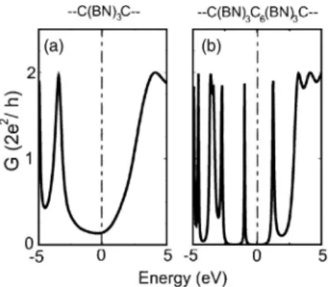
The binary compound BN can form a stable linear struc-ture and displays properties very similar to that of C-LC, except that it is a wide band gap insulator. The band gap of BN has been calculated to be 5 eV. Normally, a C-LC-BN-LC junction is a metal-semiconductor heterostructure. A periodic arrangement of CN共BN兲Mforms a superlattice; it is a semiconductor with a band gap depending strongly on N and
M. Here we consider two different devices composed from a
C-LC and BN-LC heterostructure. The first device is a short
共BN兲3 segment placed in between two C-LC electrodes. In
the case of a short segment, the BN-LC has HOMO and LUMO states separated by a wide gap. The variation of equi-librium conductance G共E兲 is illustrated in Fig. 7共a兲. A HOMO-LUMO gap of ⬃5 eV is present around the Fermi level. The double barrier structure 共BN兲3C6共BN兲3 that
con-nected two C-LC electrodes from left and right can be envis-aged as a resonant tunneling double barrier structure. The conductance G共E兲 in equilibrium in Fig. 7共b兲 reflects the electronic structure of the C-BN string heterostructure.
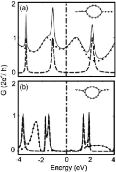
Ring structures of carbon are also present, and they are studied in several recent works.24–28We have considered the
C-R14ring structure to form a loop device. The circular ring connected to short C-LC segments from both sides has been optimized. Here we consider a symmetric and an asymmetric FIG. 6. Variation of calculated conductance G共E兲 of a segment
of C-LC having a single 共N,P,O,S兲 substitutional impurity. The dashed lines delineate the conductance of each of the two equiva-lent eigenchannels of transmission. The variation of the total con-ductance G is shown by the solid lines.
FIG. 7.共a兲 The conductance G共E兲 of a 共BN兲3barrier in between two C-LC electrodes. 共b兲 G共E兲 of a double barrier structure, 共BN兲3C6共BN兲3. EFis set to zero.
loop device and calculate the variation of their conductance. The atomic structure of these two devices is described in Fig. 8 as an inset. After the structural relaxation the circular shape of the ring is deformed in both devices. Carbon atoms of the ring connecting to the C-LC segments from both sides form planar sp2 bonds. As a result, the circular shape becomes oval. Figure 8 illustrates calculated total G共E兲 together with the contributions of two eigenchannels. In the case of a sym-metric loop the conductance is smaller than G0at EF, but we see well-defined peaks of G共E兲 at certain energies. While one
vanishes for a wide range of energies around EF, but the device conductance has some sharp peaks at some resonant values of energy.
IV. CONCLUSIONS
In this work we presented an ab initio study of transport properties of various structures and devices based on carbon and carbon-boron-nitride heterostructure strings. These struc-tures show unusual mechanical, electronic, and transport properties. We examined the effect of the electrodes and con-tact geometry, the effect of size, geometry, and strain of the string structures between electrodes.
As far as technological applications of interconnects or nanodevices are concerned, the transport properties of carbon string structures are of particular interest. We carried out an extensive analysis of the transport properties of segments of strained carbon linear chains including a different number of carbon atoms placed between different types of electrodes. In particular, the conductance calculations for a chain segment of N carbon atoms contacted to Al electrodes from both ends revealed interesting odd-even N disparity and resonant tunneling-like behavior under strain.
ACKNOWLEDGMENT
S.C. acknowledges the partial support by TÜBA 共The Turkish Academy of Sciences兲.
*Electronic address: [email protected]
1A. Aviran and M. A. Ratner, Chem. Phys. Lett. 29, 277共1974兲. 2S. Roth and C. Joachim, Atomic and Molecular Wires共Kluwer,
Dordrecht, 1997兲; Molecular Electronics, edited by J. Jortner and M. A. Ratner共Blackwell, Oxford, U.K., 1997兲.
3C. Joachim et al., Nature共London兲 408, 541 共2000兲.
4N. Agraït, J. G. Rodrigo, and S. Vieira, Phys. Rev. B 47, R12345 共1993兲.
5J. I. Pascual, J. Mendez, J. Gomez-Herrero, A. M. Baro, N. Gar-cia, and V. T. Binh, Phys. Rev. Lett. 71, 1852共1993兲.
6J. M. Krans, C. J. Müller, I. K. Yanson, T. C. M. Govaert, R. Hesper, and J. M. van Ruitenbeek, Phys. Rev. B 48, R14721 共1993兲.
7For a recent review of the subject see, S. Ciraci, A. Buldum, and I. P. Batra, J. Phys.: Condens. Matter 13, R537共2001兲. 8S. Ciraci and E. Tekman, Phys. Rev. B 40, R11969共1989兲. 9N. Agraït, G. Rubio, and S. Vieira, Phys. Rev. Lett. 74, 3995
共1995兲.
10A. Stalder and U. Dürig, Appl. Phys. Lett. 68, 637共1996兲. 11H. Mehrez and S. Ciraci, Phys. Rev. B 56, 12632共1997兲. 12O. Gulseren, F. Ercolessi, and E. Tosatti, Phys. Rev. Lett. 80,
3775共1998兲.
13M. R. Sorensen, M. Brandbyge, and K. W. Jacobsen, Phys. Rev. B 57, 3283共1998兲.
14H. Ohnishi, Y. Kondo, and K. Takayanagi, Nature共London兲 395, 780共1998兲.
15A. I. Yanson, G. R. Bolliger, H. E. van der Brom, N. Agraït, and J. M. van Ruitenbeek, Nature共London兲 395, 783 共1998兲. 16Y. Kondo and K. Takayanagi, Science 289, 606共2000兲. 17Y. Oshima, A. Onga, and K. Takayanagi, Phys. Rev. Lett. 91,
205503共2003兲.
18R. T. Senger, S. Dag, and S. Ciraci, Phys. Rev. Lett. 93, 196807 共2004兲.
19S. Iijima, Nature共London兲 354, 56 共1991兲; S. Iijima, T. Ichihashi, and Y. Ando, ibid. 356, 776共1992兲.
20M. S. Dresselhaus, G. Dresselhaus, and P. C. Eklund, Science of Fullerenes and Carbon Nanotubes 共Academic, San Diego, 1996兲.
21H. Dai, E. W. Wong, Y. Z. Lu, S. Fan, and C. M. Lieber, Nature 共London兲 375, 769 共1995兲; Y. Zhang and H. Dai, Appl. Phys. Lett. 77, 3015共2000兲; Y. Zhang, N. W. Franklin, R. J. Chen, and H. Dai, Chem. Phys. Lett. 331, 35共2000兲.
22S. Dag, E. Durgun, and S. Ciraci, Phys. Rev. B 69, 121407共R兲 共2004兲.
FIG. 8. The conductance G共E兲 of a loop device for 共a兲 symmet-ric and共b兲 asymmetric connection with C-LC electrodes. The two eigenchannels and the total conductance are shown by dashed, dot-ted, and solid curves, respectively.
23A. Karpfen, J. Phys. C 12, 3227共1979兲.
24R. O. Jones and G. Seifert, Phys. Rev. Lett. 79, 443共1997兲. 25T. Wakabayashi, M. Kohno, Y. Achiba, H. Shiromaru, T.
Mo-mose, T. Shida, K. Naemura, and Y. Tobe, J. Chem. Phys. 107, 4783共1997兲.
26E. J. Bylaska, J. H. Weare, and R. Kawai, Phys. Rev. B 58, R7488共1998兲.
27M. Saito and Y. Okamoto, Phys. Rev. B 60, 8939共1999兲. 28T. Torelli and L. Mitas, Phys. Rev. Lett. 85, 1702共2000兲. 29A. Abdurahman, A. Shukla, and M. Dolg, Phys. Rev. B 65,
115106共2002兲.
30G. Roth and H. Fischer, Organometallics 15, 5766共1996兲. 31X. Zhao, Y. Ando, Y. Liu, M. Jinno, and T. Suzuki, Phys. Rev.
Lett. 90, 187401共2003兲.
32N. D. Lang and Ph. Avouris, Phys. Rev. Lett. 81, 3515共1998兲; 84, 358共2000兲.
33N. D. Lang, Phys. Rev. B 52, 5335共1995兲; Phys. Rev. Lett. 79, 1357共1997兲.
34V. Kalmeyer and R. B. Laughlin, Phys. Rev. B 35, 9805共1987兲. 35H. Mehrez, S. Ciraci, A. Buldum, and I. P. Batra, Phys. Rev. B
55, R1981共1997兲.
36N. D. Lang and Ph. Avouris, Phys. Rev. Lett. 84, 358共2000兲.
37B. Larade, J. Taylor, H. Mehrez, and H. Guo, Phys. Rev. B 64, 075420共2001兲.
38S. Tongay, R. T. Senger, S. Dag, and S. Ciraci, Phys. Rev. Lett. 93, 136404共2004兲.
39M. C. Payne, M. P. Teter, D. C. Allen, T. A. Arias, and J. D. Joannopoulos, Rev. Mod. Phys. 64, 1045共1992兲.
40Numerical calculations have been carried out by using VASP soft-ware package: G. Kresse and J. Hafner, Phys. Rev. B 47, R558 共1993兲; G. Kresse and J. Furthmüller, ibid. 54, 11169 共1996兲. 41W. Kohn and L. J. Sham, Phys. Rev. 140, A1133共1965兲. 42J. P. Perdew, K. Burke, and M. Ernzerhof, Phys. Rev. Lett. 77,
3865共1996兲.
43J. P. Perdew and A. Zunger, Phys. Rev. B 23, 5048共1981兲. 44D. Vanderbilt, Phys. Rev. B 41, R7892共1990兲.
45H. J. Monkhorst and J. D. Pack, Phys. Rev. B 13, 5188共1976兲. 46L. V. Keldysh, Sov. Phys. JETP 20, 1018共1965兲.
47The methodology of the TRANSIESTA-C software package is de-scribed in: M. Brandbyge, J.-L. Mozos, P. Ordejón, J. Taylor, and K. Stokbro, Phys. Rev. B 65, 165401共2002兲. The software was provided by Atomistix Corp.