Hongbo Yu*, 1, Wlodek Strupinski2, Serkan Butun1, and Ekmel Ozbay1
1 Nanotechnology Research Center and Department of Physics, Bilkent University, Bilkent, 06800 Ankara, Turkey
2 Institute of Electronic Materials Technology, 01-919 Warsaw, Poland
Received 21 November 2005, revised 1 January 2006, accepted 13 January 2006 Published online 8 March 2006
PACS 73.61.Ey, 81.15.Gh
The growth of high-performance Mg-doped p-type AlxGa1–xN (x = 0.35) layers using low-pressure metal-organic chemical vapour deposition on an AlN/sapphire template is reported. The influence of growth conditions on the p-type conductivity of the AlxGa1–xN (x = 0.35) alloy was investigated. It was found that the p-type resistivity of the AlGaN alloy demonstrates a marked dependence on the Mg concentration, V/III ratio and group III element flow rate. A minimum p-type resistivity of 3.5 Ω cm for AlxGa1–xN (x = 0.35) epilayers was achieved. A Ni/Au (10 nm/100 nm) ohmic contact was also fabricated and a spe-cific contact resistivity of 8.1 × 10⁻²Ω cm2 was measured.
© 2006 WILEY-VCH Verlag GmbH & Co. KGaA, Weinheim
1 Introduction
Al-rich AlGaN alloys are currently attracting much attention since they are particularly suited for the realization of deep ultraviolet (UV) optoelectronic devices, such as light emitting diodes, laser diodes, and solar-blind photodetectors [1 – 3]. To obtain high performance from these devices, highly conductive n-type and p-type AlGaN alloys with high Al fraction are indispensable. However, compared to GaN, it is even more difficult to control the conductivity through doping in AlGaN alloys due to a higher con-centration of defects and larger ionization energy of the dopants [4]. The fabrication of p-type AlGaN with high Al content is still a significant challenge. A compromise can be reached by using methods [5, 6] such as Mg delta doping and Mg-doped strained AlGaN/GaN superlattices. Several groups have reported successful metalorganic chemical vapour deposition (MOCVD) growth of uniform p-type Al-GaN epitaxial layers using Mg as a dopant [7 – 11]. Most investigations have focused on p-type AlAl-GaN epilayers with an Al fraction that is less than 20%. Li et al. [12] obtained Mg acceptor activation energies EA of AlGaN alloy with an Al content of up to 0.27, and deduced that at an Al content of x = 0.45 the
resistivity should be as high as 2.2 × 10⁴Ω cm. Recently, Jeon et al. [13] reported p-type resistivity as low as 10 Ω cm in AlGaN epitaxial layers with an Al content of 0.3. The electrical characteristics of group III nitride epitaxial films are sensitive to the MOCVD growth conditions. It is therefore important to investigate the effect of growth parameters on the performance of p-type AlGaN.
In this paper we demonstrate the MOCVD growth conditions suitable for fabricating p-type AlGaN epilayers with high Al fraction. Based on electrical investigations of AlxGa1–xN (x = 0.35) epilayers, a minimum p-type resistivity of 3.5 Ω cm is achieved.
phys. stat. sol. (a) 203, No. 5 (2006) 869 Paper
2 Experimental
Mg-doped AlGaN epitaxial layers were grown in a low-pressure MOCVD reactor (Aixtron 200/4 HT-S). Trimethylgallium (TMGa), trimethylaluminium (TMAl), ammonia, and biscyclopentadienylmagnesium (Cp2Mg) were used as Ga, Al, N, and Mg precursors, respectively. A 15 nm thick, low-temperature (600 °C) AlN nucleation layer was deposited on a double-polished 2-inch (0001) Al2O3 substrate prior to the growth of a high-temperature (1150 °C) 0.7 µm AlN template and 0.1 µm undoped AlGaN transi-tional layer. On top of these structures, 0.3 µm thick Mg-doped AlGaN layers were grown using different growth parameters. There were no other additional conductive layers that might influence the conductiv-ity measurements.
UV optical transmission measurements were carried out using an Ocean Optics CHEM2000-UV-VIS PC plug-in fibre optic spectrophotometer in the 200 – 600 nm range. X-ray diffraction was performed using a Bruker D8 system, delivering a Cu Kα1 line. Current – voltage (I–V) transmission line model (TLM) measurements and Hall measurements (commercial Lakeshore model 7512 Hall Measurement System) were carried out to obtain the resistivity of the Mg-doped AlGaN layers. A Ni/Au (10 nm/ 100 nm) metallization contact was fabricated on the p-type AlGaN surface for the Hall measurements. Prior to the Hall measurements, the ohmic behaviour of the contacts was verified by means of I–V char-acteristics. The resistivity values from the Hall measurements were in general consistent with those from the TLM measurements. I–V measurements were carried using an HP 4142B modular DC source. To explore the influence of the growth conditions on the electrical properties of the p-type AlGaN epilayers, two series of Mg-doped AlGaN layers were grown. The TMGa flow rate was 22.5 and 40.4 µmol/min for the first and second series, respectively. The Al fraction in the AlGaN alloy was maintained at 35% in all of the samples by adjusting the TMAl flow rates to 6.7 and 17.9 µmol/min. During the growth of the AlGaN layers, the reactor pressure and growth temperature were kept at 50 mbar and 1050 °C, respectively.
3 Results and discussion
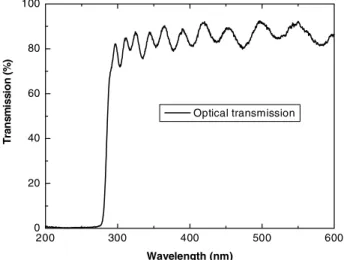
In order to determine the Al content and crystal quality of the Mg-doped AlGaN alloy, UV optical transmission was used for selected as-grown samples. As shown in Fig. 1, the optical transmission spec-trum shows a sharp cut-off at 284 nm along with well-defined Fabry – Perot oscillations due to the high quality of the material and smooth surface. One key to obtain high crystal quality of the AlGaN epilayers is the introduction of the AlN buffer. The benefits of applying an AlN epitaxial layer as buffer for defect 200 300 400 500 600 0 20 40 60 80 100 T ra n smi s si o n (% ) Wavelength (nm) Optical transmission
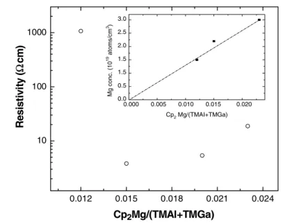
0.012 0.015 0.018 0.021 0.024 10 100 0.000 0.005 0.010 0.015 0.020 0.0 0.5 1.5 Mg conc. (10 Cp2 Mg/(TMAI+TMGa) Resist ivi ty ( Ω Cp2Mg/(TMAl+TMGa)
Fig. 2 Variation of p-type AlGaN resistivity with the Cp2Mg/(TMAl + TMGa) mole flow ratio. The in-set shows the dependence of Mg concentration of the samples on the Cp2Mg/(TMAl + TMGa) ratio.
density reduction in AlGaN have been demonstrated previously [14, 15]. GaN and AlN single layers were also measured using the same apparatus, and a value of b = 0.62 eV [16] was used for the bowing parameter. From the optical characteristics and calculations, we determined the Al content in the AlGaN alloy to be around 35%.
After growth, the Mg-doped samples were thermally activated in N2 at 850 °C for 10 min, which re-sulted in p-type conduction verified by a Hall measurement (standard Van Der Pauw). Figure 2 shows the variation of room temperature resistivity with the Cp2Mg/(TMAl + TMGa) mole flow ratio. The measured resistivity has a value of 1070 Ω cm when the Cp2Mg/(TMAl + TMGa) mole flow ratio is about 1.2 × 10⁻², and reduces sharply to 3.5 Ω cm with the mole ratio increases to 1.5 × 10⁻². With a further increase of the mole ratio, the resistivity begins to increase gradually. Jeon et al. [13] reported the viability of low-resistivity p-AlGaN doping is constrained by two competing mechanisms, namely a minimum dosage of Mg acceptors required to overcome the background defects and a doping ceiling above which structural defects occur with accompanying degradation of electrical conductivity. The resistivity variation trends for our samples are consistent with these reported results. The incorporation of Mg during AlGaN growth was studied using secondary ion mass spectroscopy (SIMS), measurements for which were carried out at Charles and Evan Inc. The inset of Fig. 2 shows the measured Mg concen-tration in AlGaN samples grown with various Cp2Mg/(TMAl + TMGa) mole flow ratios. As expected, the Mg concentration is found to increase linearly with the mole ratio. The SIMS measurements indicate that the Mg doping in AlGaN epiayers using Cp2Mg is a quite well-controlled process within the range of the experiment. Also, it is noted that there is no dependence of common impurity, such as C and O, incorporation on the Mg doping process [17].
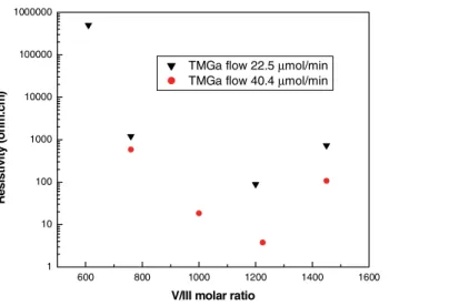
Figure 3 summarizes the room temperature resistivity of the samples from both series as a function of the V/III molar ratio. The Cp2Mg/(TMAl + TMAl) flow was kept constant so that the nominal doping concentration was not significantly different for all the samples. According to SIMS measurements of selected samples, the Mg concentration in the films is around 2.2 × 10¹⁹/cm3. The V/III ratio was cali-brated by changing the ammonia flow. As shown in Fig. 3, the variation of the resistivity as a function of V/III molar ratio shows a similar trend for both series, indicating that the resistivity of the p-type AlGaN alloy has a marked dependence on the V/III ratio. For the first series, the Mg-doped AlGaN has a high resistivity (>107Ω cm) at a V/III ratio of 610, and a minimum resistivity of 89.3 Ω cm at a V/III ratio of
phys. stat. sol. (a) 203, No. 5 (2006) 871 Paper 600 800 1000 1200 1400 1600 1 10 100 1000 10000 100000 1000000 R e s is tiv it y (o h m .c m )
V/III molar ratio
TMGa flow 22.5µmol/min
TMGa flow 40.4µmol/min
Fig. 3 (online colour at: www.pss-a.com) Resistivity of the p-type AlxGa1–xN (x = 0.35) epilayers as a function of the V/III molar ratio and group III element flow.
1200. The decrease of the resistivity of the samples with increasing V/III ratio is consistent with the compensation by nitrogen vacancies in the p-type doping of GaN [18]. Compared to the first series, the resistivity of the second series was much lower (more than one order of magnitude) which was due to the increase of the group III element precursor flow (namely the growth rate) at the same V/III ratio. The minimum resistivity (3.5 Ω cm) was achieved at a V/III ratio of 1225. Above a V/III ratio of about 1200, the resistivity values starts to increase for both series.
The exact mechanism responsible for the growth rate effect is not clear at this time. The possibility of compensation through incorporation of an external impurity was checked using SIMS measurements for C, O, H, and Si. The results show that the impurity concentrations in the two sample series are not mark-edly different. It is well known that a high V/III ratio should be maintained in order to achieve high-conductivity p-type GaN films, because compensation by nitrogen vacancies plays an important role [18]. Experimental results showed that GaN growth under N-rich conditions not only increases the Mg incorpo-ration rate but also ensures that the Mg is incorporated into substitutional Ga sites [19]. However, a rela-tively low V/III ratio should be used to obtain high crystalline quality AlGaN epilayers, by increasing the surface mobility of adsorbed Al species. We speculate that Mg atoms are more likely to replace the Ga or
-10 -5 0 5 10 -0.3 -0.2 -0.1 0.0 0.1 0.2 0.3
Low growth rate
High growth rate
Cu rren t (m A ) Applied voltage (V) Mg-doped Al0.35Ga0.65N ~ 0.3µm Undoped Al0.35Ga0.65N ~ 0.1µm
HT-AIN buffer layer ~ 0.7µm
LT-AIN nucleation ~ 15nm Sapphire substrate
3µm
Fig. 4 (online colour at: www.pss-a.com) I–V char-acteristics of the ohmic contacts to the p-type Al0.35Ga0.65N epilayers.
enhanced conductivity performance of p-type AlGaN to the following two factors: (i) improvement of AlGaN crystal quality by applying the AlN buffer layer to reduce the compensation effect from defects and scattering centres in the AlGaN epilayers; and (ii) optimization of Mg-doped AlGaN growth condi-tions, including appropriate V/III molar ratio and Mg doping concentration and a relatively high growth rate.
TLM patterns were deposited using a Ni/Au (10 nm/100 nm) alloy as ohmic contact metal. The as-deposited ohmic contacts showed non-linear behaviour for both sample series. The linearity of the I–V curves significantly improved after an anneal step that consisted of 60 s at 700 °C and 120 s at 850 °C in flowing N2 ambient. Figure 4 shows the measured I–V characteristics between two 100 µm × 200 µm TLM pads separated by a 3 µm gap. Compared to the samples with a low growth rate (TMGa flow 22.5 µmol/min), the I–V characteristics of the samples with a high growth rate (TMGa flow 40.4 µmol/min) exhibited more linear-like characteristics due to the low sheet resistivity of the p-type AlGaN layer. The TLM measurements yielded a specific ohmic contact resistivity of 8.1 × 10⁻²Ω cm2. Although this is a significantly low ohmic contact resistivity, further work should be conducted to im-prove the ohmic contact characteristics of p-type AlGaN epilayers with high Al fractions.
4 Conclusions
We have demonstrated p-type conductivity in Mg-doped AlxGa1–xN (x = 0.35) epilayers with very low impurity concentrations. The influence of growth conditions (V/III ratio, Mg doping concentration, and group III element flow rate) on the p-type conductivity was investigated. It was found that an appropriate V/III mole ratio and Mg doping concentration and a relatively high growth rate were needed to improve the electrical characteristics of the p-type AlGaN epilayers. A p-type resistivity of 3.5 Ω cm for AlxGa1–xN (x = 0.35) was obtained under the optimized growth conditions.
Acknowledgements This work was supported by EU-DALHM, EU METAMORPHOSE, EU NOE-PHOREMOST, and TUBITAK under project no. 104E090. One of the authors (E.O.) acknowledges partial support from the Turkish Academy of Sciences. The authors acknowledge Erkin Ulker for the optical measurements and Dr. Temel Buyuklimanli (Charles and Evan Inc.) for the SIMS measurements.
References
[1] J. P. Zhang, X. Hu, Y. Bilenko, J. Deng, A. Lunev, R. Gaska, M. Shatalov, J. Yang, and M. A. Khan, Appl. Phys. Lett. 85, 55 (2004).
[2] S. Ito, Y. Yamasaki, S. Omi, K. Takatani, T. Kawakami, T. Ohno, M. Ishida, Y. Ueta, T. Yuasa, and M. Taneya, Jpn. J. Appl. Phys. 43, 96 (2004).
[3] R. McClintock, A. Yasan, K. Mayes, D. Shiell, S. R. Darvish, P. Kung, and M. Razeghi, Appl. Phys. Lett. 84, 1248 (2003).
[4] T. Tanaka, A. Watanabe, H. Amano, Y. Kobayashi, I. Akasaki, S. Yamazaki, and M. Koike, Appl. Phys. Lett. 65, 593 (1994).
[5] M. L. Nakarmi, K. H. Kim, J. Li, J. Y. Lin, and H. X. Jiang, Appl. Phys. Lett. 82, 3041 (2003). [6] P. Kozodoy, M. Hansen, S. P. DenBaars, and U. K. Mishra, Appl. Phys. Lett. 74, 3681 (1999).
[7] T. Tanaka, A. Watanabe, H. Amano, Y. Kobayashi, I. Akasaki, S. Yamazaki, and M. Koike, Appl. Phys. Lett. 65, 593 (1994).
[8] M. L. Nakarmi, K. H. Kim, M. Khizar, Z. Y. Fan, J. Y. Lin, and H. X. Jiang, Appl. Phys. Lett. 86, 092108-1 (2005).
phys. stat. sol. (a) 203, No. 5 (2006) 873 Paper
[10] G. Kipshidze, V. Kuryatkov, B. Borisov, Y. Kudryavtsev, R. Asomoza, S. Nikishin, and H. Temkin, Appl. Phys. Lett. 80, 2910 (2002).
[11] R. Y. Korotkov, J. M. Gregie, and B. W. Wessels, Appl. Phys. Lett. 78, 222 (2001).
[12] J. Li, T. N. Oder, M. L. Nakarmi, J. Y. Lin, and H. X. Jiang, Appl. Phys. Lett. 80, 1210 (2002).
[13] S.-R. Jeon, Z. Ren, G. Cui, J. Su, M. Gherasimova, J. Han, H.-K. Cho, and L. Zhou, Appl. Phys. Lett. 86, 082107 (2005).
[14] S. Arulkumaran, M. Sakai, T. Egawa, H. Ishikawa, T. Jimbo, T. Shibata, K. Asai, S. Sumiya, Y. Kuraoka, M. Tanaka, and O. Oda, Appl. Phys. Lett. 81, 1131 (2002).
[15] B. Zhang, T. Egawa, H. Ishikawa, Y. Liu, and T. Jimbo, J. Appl. Phys. 95, 3170 (2004).
[16] S. R. Lee, A. F. Wright, M. H. Crawford, G. A. Petersen, J. Han, and R. M. Biefeld, Appl. Phys. Lett. 74, 3344 (1999).
[17] Hong Bo Yu, E. Ulker, and E. Ozbay, accepted by J. Cryst. Growth.
[18] P. Kozodoy, S. Keller, S. P. DenBaars, and U. K. Mishra, J. Cryst. Growth 195, 265 (1998).
[19] J. W. Orton, C. T. Foxon, T. S. Cheng, S. E. Hooper, S. V. Novikov, B. Ya. Ber, and Yu. A. Kudriavtsev, J. Cryst. Growth 197, 7 (1999).