Simulation and micro-fabrication of optically switchable
split ring resonators
T.F. Gundogdu
a,*
, Mutlu Go¨kkavas
b, Kaan Gu¨ven
b, M. Kafesaki
a,
C.M. Soukoulis
a,c, Ekmel Ozbay
baInstitute of Electronic Structure and Laser, Foundation for Research and Technology, Hellas and Department of
Materials Science and Technology, University of Crete, Greece
bNanotechnology Research Center, Department of Physics, Department of Electrical and Electronics Engineering,
Bilkent University, Bilkent, Ankara 06800, Turkey
cAmes Laboratory-USDOE and Department of Physics and Astronomy, Iowa State University, Ames, IA 50011, USA
Received 15 February 2007; received in revised form 3 July 2007; accepted 4 July 2007 Available online 12 July 2007
Abstract
The effect of conductivity variation as a proposed method for the investigation of photoconductive switching properties of split ring resonators (SRRs) is simulated. Three different systems that are applicable under certain fabrication and/or optical excitation conditions are described. The simulated transmission spectrum indicates that for a large range of dark conductivity values, complete switching of the SRR resonance is possible. One of the simulated systems, involving split ring resonators on Si substrate, was fabricated and characterized. The transmission spectrum of that system was measured, with the Si in its high-resistivity state, and a
60 dB dip between 108 and 115 GHz, due to SRRs magnetic resonance, was observed. # 2007 Published by Elsevier B.V.
Keywords: Left handed materials; Split ring resonators; Photoconductive; Simulation
Veselago developed the idea of left-handed (LH) materials in 1968[1]. These materials exhibit the unique physical property of having both negative electrical permittivity (e) and negative magnetic permeability (m) over a common frequency band. Left handed metamater-ials generated a great interest, partly due to the properties of these materials which are not observed in naturally occurring materials. These include negative refractive index, artificial magnetism, super focusing, and reduced lens aberrations[1–5]. Since the first demonstration of LH metamaterials [4], different structures that exhibit equivalent properties have been proposed[6]; however
the initial structure consisting of the periodic arrangement of split ring-resonators (SRRs) and metallic wires remains the mostly studied. The wires provide the negative electric permittivity, (e),[7]whereas the SRR-elements generate the negative magnetic permeability (m) response[2]. The SRR consists of metallic rings with gaps that act like a capacitor–inductor (LC) circuit when a magnetic field component is perpendicular to their plane. Due to the resonant circular currents in the rings they exhibit a resonance at vm= 1/(LC)1/2 associated with
resonant circular currents in the SRR rings[8–10]. It was also demonstrated that besides for a magnetic field that is perpendicular to the SRR plane, the existence of an electric field parallel to the gaps of the SRR can couple to the magnetic resonance and excite an oscillating resonant current around the rings. This phenomenon is described as
www.elsevier.com/locate/photonics
* Corresponding author.
E-mail address:[email protected](T.F. Gundogdu).
1569-4410/$ – see front matter # 2007 Published by Elsevier B.V. doi:10.1016/j.photonics.2007.07.001
the electric excitation of the magnetic resonance of the SRR[11–13].
A significant challenge in LH materials research is the tuning and switching of such materials. Recently,
Padilla et al. reported the all-optical switching of the electromagnetic response of SRRs at THz frequencies by the photoexcitation of carriers in the sample substrate[14]. Previously, we had demonstrated a LH
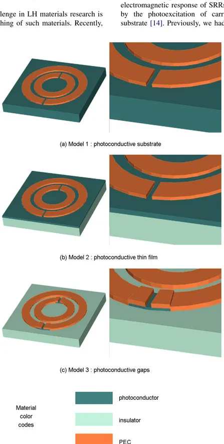
composite metamaterial operating at 100 GHz[15]. In the present paper, we report our work conducted on the design, simulation and micro-fabrication of optically switchable SRRs around 100 GHz operation frequency. For simulations a commercially available software (Microwave Studio) employing the finite integration method to solve Maxwell’s equations was used [16]. Simulations were performed for three different physical configurations (herein after referred to as models). These three models are illustrated inFig. 1a–c. The left panels shown inFig. 1illustrate the general view of one metamaterial unit cell, whereas the right panels show the gap region in closer detail. In the first model (Fig. 1a), the effect of a photoconductive substrate is investigated by way of increasing the conductivity (s) of the substrate region to symbolize illumination with higher optical powers. The fabrication sequence for this model is identical to the one described in our earlier work[15], using photoconductive substrates instead of glass. In comparison, model 2 (Fig. 1b) employs insulating substrates. Split ring resonators are placed atop thin films of deposited or epitaxially grown photoconductive material. It is noteworthy that model 2 is also applicable to photoconductive substrates for which the optical absorption coefficient (a) is so high that the photogeneration of carriers is confined to a thin surface layer. On the other hand, model 1 better suits photoconductive substrates with low a, due to the possibility of photogeneration throughout the entire substrate. The last model includes photoconductive material in a localized area slightly larger than the split ring gap regions beneath the gaps. To realize such a structure, a two step micro-fabrication sequence must be employed: first the photoconductive gap regions must be defined by way of chemical or physical etching, followed by the deposition of the resonator pattern. Even when the entire substrate is illuminated, photo-generation for such a structure is limited to the gap regions only. In addition, model 3 also describes those
situations where the photogeneration of carriers is localized at the gap region by use of a focused laser beam, even if the photoconductive layer or substrate is not patterned. Models 2 and 3 are both appropriate for describing front- and substrate-side optical illumina-tion, whereas model 1 is suited only for front-side illumination because of the thick photoconducting substrate.
The exact dimensions used in the simulations are listed inTable 1. For models 2 and 3, the dimensions are identical to the structure in[15]. This structure is known to yield a magnetic resonance dip (m < 0) between 95 and 108 GHz when fabricated on glass substrates (e = 4.82). For model 1, the structure is rescaled such that the resonance will occur around 90–100 GHz when fabricated on Si substrates (e = 11.9). In models 2 and 3, the thin photoconductive layer is modeled by a 1 mm-thick ZnO (e = 8.5) film. For all models, the substrate thickness is 150 mm, and the 0.5 mm-thick conductors
Table 1
Simulation parameters for the three models inFig. 1
Model 1 Model 2 Model 3
Substrate material Si (e = 11.9) Glass (e = 4.82) Glass (e = 4.82)
Substrate thickness 150 mm 150 mm 150 mm
Photoconductive layer Substrate 1 mm-thick ZnO (e = 8.5) 1 mm-thick ZnO (e = 8.5) across gaps
Periodicity in SRR plane ak= aE 164.2 mm 262.7 mm 262.7 mm
Metal thickness 0.5 mm 0.5 mm 0.5 mm
Split ring gap 4.5 mm 7.2 mm 7.2 mm
Inner ring inner radius 26.9 mm 43 mm 43 mm
Inner ring outer radius 42 mm 67.2 mm 67.2 mm
Outer ring inner radius 50.4 mm 80.7 mm 80.7 mm
Outer ring outer radius 67.2 mm 107.5 mm 107.5 mm
Fig. 2. Calculated magnetic resonance for the three models when no optical excitation is present. The pronounced transmission dips in the spectra are due to the SRRs magnetic resonance. Inset shows the orientation of the E-field, H-field, and wave vector.
of the resonators are modeled as perfectly conducting. The schematic SRR unit cell and the relative orientation of the electromagnetic excitation are shown in the inset ofFig. 2. The magnetic field is perpendicular to the SRR plane and the directions of electric field and propagation are as shown. For all of the simulations; the number of unit cells employed was chosen as 3 in the propagation direction and 1 in the other two directions, in order to limit the computational cost of simulations. Boundary conditions were defined by setting tangential electric/ magnetic fields equal to zero in the boundaries perpendicular to the direction of the electric/magnetic fields. The calculated transmission spectra for the three SRR models when there is no illumination are shown in Fig. 2. A magnetic resonance dip is observed at 88 GHz for model 2, at 90 GHz for model 3, and at 95 GHz for model 1. Although the in-plane geometry of models 2 and 3 are identical, the 2 GHz shift in the resonance frequency is expected due to the presence/absence of the thin photoconductive layer which contributes by a different dielectric constant. The magnetic nature of the resonance dip is verified by closing the SRR gaps by perfect electrical conductor (PEC) in simulations and in observation of the disappearance of the dip. For all three models the minimum of the transmission dip is
observed around 60 dB.
Next, the effect of photoexcitation was investigated for the three models by varying the conductivity (s) of the respective photoconductive layers. Because of the limitations imposed by the simulation toolbox, the conductivity was assumed to be a constant throughout the photoconductive layer. Although this assumption may not model the optical absorption process accurately for some cases, it is a valid approximation for low absorption coefficients and/or thin absorbing films. Fig. 3 shows the transmission spectra calculated for model 1 as a function of the substrate conductivity. The two lower s values (0.1 and 1 S/m) represent the typical conductivity values for commercial Si substrates. It is observed that the transmission dip occurs at 53 dB and 36 dB for s = 0.1 S/m and s = 1 S/m, respectively. When the conductivity of the substrate is increased gradually (equivalent to a gradual increase of photo-generation throughout the entire substrate), the reso-nance is observed to disappear gradually. For a sufficiently large increase in conductivity, the resonance can be completely switched off. For example, an increase from 1 S/m to 30 S/m in s results in the total
disappearance (dotted purple curve) of the 36 dB
resonance (solid red curve). For s = 30 S/m, the transmission level drops to 15 dB as a result of the increased total loss in the structure.
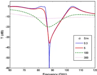
Analogous calculations to the one described above were performed also for models 2 and 3, where the effect of a conductivity increase of the thin photo-conducting layer was investigated. Fig. 4 shows the transmission spectra that were calculated for model 2. The two lower s values (0.3 S/m and 5 S/m) represent the range of conductivity values when the structure is not illuminated with sufficient optical power. It is observed that the transmission dip occurs at 60 dB and 36 dB for s = 0.3 S/m and s = 5 S/m, respectively. As the conductivity of the thin film photoconductive layer is increased the resonance is observed to disappear gradually. If the photoconductivity is increased as much as 300 S/m (dotted purple line), the resonance dip disappears. Similar to the model 1, the transmission
Fig. 3. Calculated transmission spectra for simulation model 1 as a function of the conductivity of the photoconducting substrate.
Fig. 4. Calculated transmission spectra for simulation model 2 as a function of the conductivity of the thin photoconducting film.
level of the structure drops to 10 dB for this high conductivity value as a result of the loss associated with the thin conducting layer. Fig. 5shows the calculated transmission spectra for model 3. It is observed that the non-illuminated transmission dip occurs at 54 dB and 35 dB for s = 1 S/m and s = 10 S/m, respectively. When the conductivity of the photoconductive material across the gaps is increased, the resonance is observed to disappear gradually in similar fashion to the other two models. Finally, a 100-fold increase of conductivity, from the non-illuminated value of 10 S/m (solid red curve) to 1000 S/m (solid purple curve), causes the complete switch off of the resonance. In contrast to the first two models, where the transmission levels away from the magnetic resonance showed a considerable drop by increasing conductivity, here the transmission
level remains at around 5 dB even for 1000 S/m
conductivity.
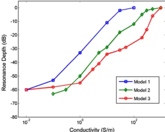
Comparing the results of Figs. 3–5, several
observations are made: First, the conductivity value to achieve complete switching is highest for model 3 and lowest for model 1. Similarly, the proportional increase in conductivity required to achieve any fixed amount (in dB) of switching is also highest for model 3 and lowest for model 1.These observations are better displayed inFig. 6, wherein the depth of the respective resonance dips are plotted for the three models as a function of conductivity. It is seen that the resonance depth is highest for model 3 (least switching), and lowest for model 1 (largest switching). This is expected since the volume where the material conductivity is modulated is highest in model 1 and lowest in model 3. However, it has to be noted that model 3 is still the most
efficient when required photoconductivity change multiplied by the photo-absorbing volume is consid-ered. This is the proper way of comparison, because the product of the required photoconductivity change and optically absorbing volume is directly proportional to the number of absorbed photons, hence to the required incident power. Fig. 7compares calculated resonance depths for the three models as a function of the product of photoconductivity and optically absorbing volume. It is observed fromFig. 7that model 3 is approximately four and two orders of magnitude more efficient than models 1 and 2, respectively.
Having defined the required designs and conditions to achieve satisfactory switching, we proceeded to the
Fig. 5. Calculated transmission spectra for simulation model 3 as a function of the conductivity of the photoconducting material covering the SRR gaps.
Fig. 6. Calculated resonance depth (dB) for the three models as a function of conductivity.
Fig. 7. Calculated resonance depth (dB) for the three models as a function of the product of optically absorbing volume and photoinduced conductivity (this product is proportional to the absorbed optical power).
fabrication of those systems and the experimental validation of the results described above. Here, we will report on the fabrication and the non-illumination characterization of the model 1 described above. Split-ring resonator arrays were fabricated on 450 mm-thick Si substrates with 2 S/m conductivity. First, the model 1
SRR pattern described in Table 1 was defined by
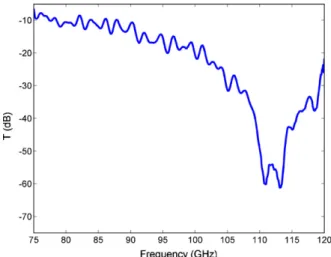
photolithography. Then, 100 A˚ Ti/5000 A˚ Au metal patterns were deposited by thermal evaporation and subsequent lift-off.Fig. 8(a) shows several examples of fabricated samples. The larger samples to the left and bottom of the figure are designed for lower frequency experiments. The stack of planar samples sandwiched between glass spacers is the bulk 100 GHz test sample. A detail of one of the planar samples can be seen in Fig. 8(b). The millimeter wave measurements were carried out by using a HP 8510C network analyzer. First, the signal from the network analyzer was converted up in frequency to the 75–115 GHz range by using a multiplier source unit. The signal was transmitted by a horn antenna and the transmission through a stack of samples was measured by a second horn antenna and mixing detector combination. Stack-ing of approximately 20 samples was necessary in order to cover the entire antenna aperture. Fig. 9shows the measured transmission through 36 consecutive SRRs in the propagation direction. The measurement orientation was same as that is indicated in Fig. 1. A 60 dB resonance dip was observed between 108 GHz and 115 GHz. The spectral shift from simulations is due to deviation from the design during fabrication. The transmission level for non-resonant frequencies was around 20 dB, which is consistent with the increased loss associated with the large number of SRRs in the propagation direction. To test the optical switching, it was necessary to be able to illuminate the sample. However, the stack of samples was too tightly packed and had no optical clearance. We were not able to
observe the SRR resonance when the stack was disassembled and a single layer of substrate was tested. This is because a single layer is too thin to cover the antenna aperture. We are currently investigating different stack geometries where we will be able to effectively cover the antenna aperture as well as have enough optical clearance to test switching character-istics.
In conclusion, we simulated the effect of conductiv-ity variation as a proposed method for the investigation of the photoconductive switching properties of SRRs. We described three different simulation models that are applicable under certain fabrication and/or optical excitation conditions. We calculated that for a large range of dark conductivity values, it is possible to achieve switching by the careful selection of the appropriate model and excitation conditions. We fabricated SRR structures on Si substrates and measured
a 60 dB resonance dip between 108–115 GHz. Next,
these structures will be tested under optical excitation.
Fig. 8. Fabricated samples: (a) larger, lower frequency samples, and the stack of planar samples for 100 GHz operation. (b) Photomicrograph of sample.
Fig. 9. Measured transmission spectra of SRRs fabricated on Si substrates according to model 1.
This work is supported by the European Union under the projects METAMORPHOSE, EU-NoE-PHOREMOST, by TUBITAK under Projects Nos. 104E090, 105E066, 105A005, 106A017, by Ames
Laboratory (Contract No. W-7405-Eng-82) and
Defence Advanced Research Projects Agency (Contract No. MDA 972-01-2-0016), by the AFOSR under MURI Grant FA9550-06-1-0337, and by the Greek Ministry of Education Pythagoras Project. The research of C.M. Soukoulis is further supported by the Alexander von Humboldt Senior Scientist Award 2002. One of the authors (E.O.) also acknowledges partial support from the Turkish Academy of Sciences.
References
[1] V.G. Veselago, Sov. Phys. Usp. 10 (1968) 504.
[2] J.B. Pendry, A.J. Holden, D.J. Robbins, W.J. Stewart, IEEE Trans. Microw. Theory Tech. 47 (1999) 2075.
[3] J.B. Pendry, Phys. Rev. Lett. 85 (2000) 3966.
[4] R.A. Shelby, D.R. Smith, S. Schultz, Science 292 (2001) 77.
[5] D. Schurig, D.R. Smith, Phys. Rev. E 70 (2004) 065601(R). [6] V.M. Shalaev, W. Cai, U.K. Chettiar, H.K. Yuan, A.K. Sarychev,
V.P. Drachev, A.P. Kildishev, Opt. Lett. 30 (2005) 3356. [7] J.B. Pendry, A.J. Holden, W.J. Stewart, I. Youngs, Phys. Rev.
Lett,. 76 (1996) 4773.
[8] N. Katsarakis, T. Koschny, M. Kafesaki, E.N. Economou, E. Ozbay, C.M. Soukoulis, Phys. Rev. B 70 (2004) 201101(R). [9] K. Aydin, K. Guven, M. Lei Zhang, C.M. Kafesaki, E. Soukoulis,
Ozbay, Opt. Lett. 29 (2004) 2623.
[10] R.A. Shelby, D.R. Smith, S.C. Nemat Nasser, S. Schultz, Appl. Phys. Lett. 78 (2001) 489.
[11] P. Gay-Balmaz, O.J.F. Martin, J. Appl. Phys. 92 (2002) 2929. [12] N. Katsarakis, T. Koschny, M. Kafesaki, E.N. Economou, C.M.
Soukoulis, Appl. Phys. Lett. 84 (2004) 2943.
[13] N. Katsarakis, G. Konstantinidis, A. Kostopoulos, R.S. Penciu, T.F. Gundogdu, M. Kafesaki, E.N. Economou, T.H. Koschny, C.M. Soukoulis, Opt. Lett. 30 (2005) 1348–1350.
[14] W.J. Padilla, A.J. Taylor, C. Highstrete, M. Lee, R.D. Averitt, Phys. Rev. Lett. 96 (2006) 107401.
[15] M. Go¨kkavas, K. Gu¨ven, I. Bulu, K. Aydın, R.S. Penciu, M. Kafesaki, C.M. Soukoulis, E. Ozbay, Phys. Rev. B 73 (2006) 193103.
[16] R.S. Penciu, M. Kafesaki, T.F. Gundogdu, E.N. Economou, C.M. Soukoulis, Photon. Nanostr. 4 (2006) 12–16.