REFRACTIVE INDEX TUNING WITH
BURSTEIN-MOSS EFFECT IN INDIUM
NITRITE UNDER PHOTOEXCITATION
a thesis
submitted to the program of physics
and the institute of engineering and science
of bilkent university
in partial fulfillment of the requirements
for the degree of
master of science
By
Cem Murat Turgut
August, 2009
I certify that I have read this thesis and that in my opinion it is fully adequate, in scope and in quality, as a thesis for the degree of Master of Science.
Assoc. Prof. Dr. Ceyhun Bulutay (Advisor)
I certify that I have read this thesis and that in my opinion it is fully adequate, in scope and in quality, as a thesis for the degree of Master of Science.
Prof. Dr. Atilla Aydınlı
I certify that I have read this thesis and that in my opinion it is fully adequate, in scope and in quality, as a thesis for the degree of Master of Science.
Prof. Dr. Ra¸sit Turan
Approved for the Institute of Engineering and Science:
Prof. Dr. Mehmet B. Baray
Director of the Institute Engineering and Science
ABSTRACT
REFRACTIVE INDEX TUNING WITH
BURSTEIN-MOSS EFFECT IN INDIUM NITRITE
UNDER PHOTOEXCITATION
Cem Murat Turgut M.S. in Physics
Supervisor: Assoc. Prof. Dr. Ceyhun Bulutay August, 2009
The band filling effect due to free carriers introduces a shift in the absorption edge, which in turn modifies the refractive index of the medium through the Kramers-Kronig relation. This is known as the Burstein-Moss effect. Based on the full band pseudopotential electronic structure calculations, we demonstrate that Burstein-Moss effect will be crucial in the design of InN based lasers. The primary reason is the small effective mass and the strong nonparabolicity of the conduction band of InN where the shift in the absorption edge is more than 0.5 eV for an electron density of the order of 1019 cm−3. On the other hand,
for the case of valence band, the shift in the absorption edge is approximately 0.04 eV. However due to high density of states at the edge of the valence band, also this shift becomes crucial since it opens intraband transitions in the medium. In the case of laser structures, the Burstein-Moss effect in both conduction and valence bands needs to be considered. Furthermore, we take into account the band gap renormalization due to high free carrier concentration. For the case of semiconductor laser structures, which can be also considered as an n-p junction, we predict about 2% change in the refractive index for a wavelength 1.55 µm at an electron-hole density of 1019 cm−3. When we compare photoexcited (i.e.,
n = p) InN with n-type doped InN, in the former case the intraband transitions in the valence band which is a result of Γv
5 → Γv6 transition, partially cancels
the Burstein-Moss effect. Our findings can also have direct implications for InN based optical modulators.
Keywords: Refractive index change, semiconductor optics, band filling, band gap renormalization.
¨
OZET
IS¸IK UYARIMI ALTINDA ˙IND˙IYUM N˙ITRAT’ IN
BURSTEIN-MOSS ETK˙IS˙IYLE KIRINIM ˙IND˙IS˙INDEK˙I
DE ˘
G˙IS¸˙IM
Cem Murat Turgut Fizik, Y¨uksek Lisans
Tez Y¨oneticisi: Do¸c. Dr. Ceyhun Bulutay A˘gustos, 2009
Serbest ta¸sıyıcılar sebebiyle olu¸san band dolum etkisi, so˘gurma e¸si˘ginde kaymaya sebep olur ve bu de˘gi¸siklik, Kramers-Kronig ili¸skisiyle, maddenin kırınım indisini de˘gi¸stirir. Bu, Burstein Moss etkisi olarak da bilinir. T¨um Brillouin b¨olgesi boyunca elektronik bant yapısı g¨or¨un¨ur potansiyel yakla¸sımıyla elde edilmi¸stir ve bu hesaplamalara dayanarak, InN temelli lazerlerin tasarımında Burstein Moss etkisinin can alıcı oldu˘gu g¨osterilmi¸stir. ˙Iletkenlik bant kenarındaki parabolik olmayan enerji da˘gınım ba˘gıntısı ve k¨u¸c¨uk etkin k¨utle, bu etkinin en ba¸sta ge-len sebeplerindendir. 1019 cm−3 mertebesindeki elektron yo˘gunlu˘gu iletkenlik
bandının so˘gurma e¸si˘ginde, 0.5 eV’tan daha fazla kaymaya sebep olur. De˘gerlik bandında bu de˘ger 0.04 eV olmasına ra˘gmen, bant kenarındaki y¨uksek durum yo˘gunlu˘gu, so˘gurma e¸si˘gindeki bu k¨u¸c¨uk kaymayı ¨onemli kılmaktadır. Lazer yapılarında, Burstein Moss etkisi hem iletkenlik hem de de˘gerlik bandı g¨oz ¨on¨une alarak de˘gerlendirilmelidir. Buna ilaveten, y¨uksek yo˘gunluktaki serbest ta¸sıyıcılar bant aralı˘gında daralmaya neden olur. B¨ut¨un bu etkilerin yanında plazma etkisi de hesaba katılarak, kırınım indisindeki de˘gi¸sim hesaplanmı¸stır. Burstein Moss etkisiyle, tipik lazer dalgaboyu olan 1.55 µm’de, yarıiletken maddenin kırınım indisinde yakla¸sık 2% de˘gi¸sim tahmin ediyoruz. Sonu¸clarımızı n-tipi InN ile kar¸sıla¸stırdı˘gımızda, Γv
5 → Γv6 ge¸ci¸sinden kaynaklanan yo˘gun bant i¸ci ge¸ci¸sleri
n-p tipi InN’ta Burstein Moss etkisini kısmen kaybettirmektedir. Bulgularımızın, InN temelli optik mod¨ulat¨orler i¸cin de ilgili olaca˘gı d¨u¸s¨un¨ulmektedir.
Anahtar s¨ozc¨ukler : Kırınım indis de˘gi¸simi, yarıiletken opti˘gi, bant dolumu, bant aralı˘gında daralma.
Acknowledgement
I am very glad to thank Assoc. Prof. Dr. Ceyhun Bulutay who has been a great support in the process of my thesis. He is beyond a thesis supervisor. I take him as a role model in my career. Moreover, I am grateful to my group members for the fish sandwiches. I would like to thank Halime Kutlutan for the language support, Levent Suba¸sı for Linux support, ¨Umit Kele¸s and Duygu Can for friendly conversations, Emre Ta¸sgın for tea services, Kurtulu¸s Abak for being a co-pilot in our trips, Hasan S¸ahin for the cold beverages. I send lots of love to Ceydos, Deniz and Engin who have been great online supports. I would like to thank my family for being great supporters of my continuing to be an academician, and I would like to mention that there are many names that I do not forget but cannot write here. It would be a very long list then.
The financial support by the UNAM-Regpot Project (Grant No:203953) for attending the E-MRS conference in June 2009 is acknowledged.
This thesis is dedicated to Tu˘g¸ce, who has stood up to the difficulties through-out my undergraduate and master life with me.
Contents
1 Introduction 1
1.1 Band Filling Effect . . . 1
1.2 Burstein-Moss Effect in Semiconductor Physics . . . 2
1.3 Band Filling Effect in InN . . . 3
1.4 Modulator Applications . . . 4
1.5 Plan of the Thesis . . . 5
2 Electro-Optic Media 6 2.1 Electro-Optic Effects . . . 7
2.2 Pockels Effect . . . 7
2.3 Kerr Effect . . . 9
2.4 Quantum Confined Stark Effect . . . 12
2.5 Franz-Keldysh Effect . . . 14
2.6 Quantum Confined Pockels Effect . . . 15
2.7 Burstein-Moss Effect . . . 15
CONTENTS vii
2.8 Purcell Effect . . . 17
3 Semiconductor Lasers 19 3.1 Basic Structure . . . 20
3.2 Photoexcitation and Attainment of Quasi-Equilibrium . . . 20
3.3 Carrier Distribution . . . 22
3.4 Chirp . . . 23
4 Further Technical Preliminaries 25 4.1 Brillouin-Zone Integrations . . . 25
4.1.1 Lehmann-Taut Method . . . 26
4.1.2 Application to Density of States . . . 28
4.1.3 Effective Mass and Dielectric Tensors . . . 29
4.2 Van Hove Singularities . . . 30
4.3 Kramers-Kronig Relation . . . 32
5 Band Gap Renormalization 34 5.1 Plasmon-Pole Approximation . . . 35
5.2 Vashishta-Kalia Model . . . 36
5.3 Random Phase Approximation . . . 38
5.4 Band Tailing Effect . . . 39
CONTENTS viii
6.1 Electronic Structures . . . 41 6.2 Brillouin Zone Integration . . . 42 6.3 Results . . . 44
List of Figures
2.1 Basic illustration of an passing light though the electro-optic medium which is modulated by an external voltage. . . 8 2.2 In the presence of the electric field, band gap of the material is
re-duced which enables in tunnelling of the electron to the conduction band. . . 12 2.3 As the carrier densities increase in both valence band and
con-duction band, excitation of an electron to the concon-duction band requires more energy. . . 16 2.4 As the carrier densities increase in both valence band and
conduc-tion band, due to the many body effects band gap is renormalized. 17
3.1 Basic structure for the semiconductor laser. . . 20 3.2 Photoexcitation in semiconductor lasers. . . 21 3.3 (a) shows the up-chirp with increasing instantaneous frequency,
(b) shows the down-chirp with decreasing instantaneous frequency. 24
4.1 Filling of Brillioun zone with tetrahedra. . . 26 4.2 First Brillioun zone of the wurtzite lattice and its IBZ . . . 27 4.3 Meshing on the IBZ . . . 27
LIST OF FIGURES x
4.4 Different intersections of a tetrahedron with three different con-stant energy surfaces. . . 29 4.5 Different types of van Hove singularities. The arrows indicate the
energies where the singularities exist. The circles shows the dis-continuities in the derivative of the density of states . . . 31
5.1 The dashed lines are the VK formulation for the band gap renor-malization. Solid lines are the formulation of Sernelius approach. The symbol points are taken from the experimental data in Ref. [36]. . . 37 5.2 Band gap renormalization for different types of InN with different
type of methods. . . 39
6.1 Band structure of InN (solid) and GaN (dashed) computed by using empirical pseudopotential method [50]. . . 43 6.2 Density of states for InN. The inset gives us a view in a narrow
en-ergy range for DOS. Band filling effect is given for different carrier densities. . . 44 6.3 Imaginary part of the dielectric function of InN. The inset shows
the behaviour of the function in a wider energy range. . . 45 6.4 A basic illustration for the transitions of electrons by absorbing
photons. a shows interband transitions and b shows intraband transitions. . . 46 6.5 Real part of the dielectric function of InN. The inset shows the
behaviour of the function in a wider energy range. . . 47 6.6 Carrier density dependent change in the refractive index of n-doped
List of Tables
Chapter 1
Introduction
1.1
Band Filling Effect
The history behind this thesis goes back to 1950’s. The first problem is encoun-tered with the Indium including compounds in 1953. The measured band gap (∆Eg) of Indium Antimonide (InSb) had divergent values. Tatenbaum and Briggs
tried to explain this anomalous behaviour of InSb [1]. For different concentration of impurity levels, they measured different band gap values by means of photo absorption experiment and according to their measurement they concluded that the reason for this anomalous behaviour was related to the impurities however, they couldn’t explain the physical reasons [1].
In the same year 1953, Burstein remeasured the band gap of InSb [2], and he also confirmed the absorption values for InSb reported by Tatenbaum and Briggs’ work. However, he explained the anomalous band gap behaviour with a different perspective. The reason was explained as being due to the small effective mass of InSb rather than an impurity effect. The sharp curvature in the bottom of the conduction band results in the small electron effective mass and small density of states at that region. For the relatively small electron densities, the Fermi level of the semiconductor lies above the conduction band as a result of filling available density of states and the Fermi level increases rapidly with the
CHAPTER 1. INTRODUCTION 2
increasing electron density [2]. As the carrier density increases, the absorption energy from valence band to Fermi energy level increases. At the same time, Moss independently proposed the same reason for the unusual band gap of InSb [3]. Hence this is named as the Burstein Moss effect which is generally observed in the semiconductors which have small effective masses. The importance of this effect for applied physics is realized in 1960’s, as it gives a chance to obtain different optical properties with the same semiconductor.
1.2
Burstein-Moss
Effect
in
Semiconductor
Physics
By doping the semiconductor, one can modulate the absorption edge, refractive index, emission of the medium by means of Burstein-Moss effect. In 1969, Dapkus and his colleagues modulated the laser transition energies and wavelength limits of GaAs by n-type doping [4]. With a doping level Nd∼ 1018donors/cm3, photon
energy of emitted laser light increases rapidly. This is because the Fermi level in the conduction band moves up with the doping level. Interband recombination processes predominantly occur from the Fermi level in the conduction band to the valence band edge. So n-type semiconductor lasers lase at higher energies compared to the undoped semiconductor lasers. On the other hand, the effect of donors and the acceptors in the band structure should be considered since they can open new transition levels in the forbidden gap of the medium [4].
The effect of band filling on the absorption coefficient is calculated for GaAs based lasers in Bell Laboratories in 1975 [5]. The measurements were made on highly doped n-type samples with a free electron concentration∼ 6.7×1018cm−3.
By using the reflectance data, together with the Kramers-Kronig relation, they obtained the absorption coefficient. The result showed that absorption is strongly dependent on the impurity concentration. A similar work was done in 2001 for InSb [6]. Through the Kramers-Kronig relations carrier dependent absorption spectra and the refractive index change is calculated in correction to the laser structures. Compared to the intrinsic semiconductor, high doping tends to reduce
CHAPTER 1. INTRODUCTION 3
the refractive index [6].
In 1989, Schubert applied Burstein Moss effect to the quarter wave semicon-ductor plates of InP-InGaAs. As the carrier density increased, they filled the available states in the conduction band for n-type semiconductors. As a result of band filling, states at the bottom of the conduction band were blocked, so the electron excitation from valence band to these states was reduced for a photon energy with corresponding wavelength. So the reflectivity at this wavelength was increased [7]. This effect was used for passive mode locking and Q switching of an erbium laser at a wavelength 3 µm by using InAs. At room temperature band gap of InAs is 0.35 eV which corresponds a wavelength 3.54 µm however n-type InAs shows a band to band transitions at 0.44 eV with a wavelength 2.8 µm [8]. Also in the same year, this effect was used to modulate the waveguide in a two dimensional system. Junction field-effect transistor was incorporated to an optical waveguide and the gates modulated the light by band filling effect. By applying reverse gate-source bias Vgs and drain-source bias Vds, free carriers
doped the waveguide, and as the free carrier concentration increased band filling effect was observed. As a result the absorption and the refractive index of the medium was modulated [9].
A more recent application of band filling effect was published in 2007 by Yang. Mercury-cadmium-telluride (HgCdTe) is an important semiconductor which is used for infrared photodetectors. By doping the material n-type, the luminescence peak of the semiconductor showed a blue shift with an amount of∼ 40 meV [10]. These are the examples of Burstein-Moss effect which are used in semiconductor physics.
1.3
Band Filling Effect in InN
Band filling effect can be observed in the semiconductors which have small elec-tron effective masses and low density of states at the conduction band edge. As it is seen above, In-included compounds are the best candidates for this effect.
CHAPTER 1. INTRODUCTION 4
Indium is a III-A group member in periodic table and makes compounds with V-A group members. In the last decades III-V semiconductors have been the focus of the attention of the semiconductor physics society because it has a wide range technological applications. Especially III-nitrite semiconductors attract attention for gallium nitride’s applications in optoelectronics. Among III-nitrite semiconductors, InN has been of of interest in recent years.
InN preserved its mysteries for decades. Like InSb, the band gap of InN ex-hibits an anomalous behaviour. This effect first was observed in InN by Trainor and Rose [11] in 1974 and between 1985-86 it was intensively studied by Tans-ley and FoTans-ley for InN films growth by RF sputtering [12]. The increase in the absorption edge was empirically fitted as
Egm = Eg+ 2.1× 10⁻⁸n1/3 eV,
where Egm is the measured apparent band gap and n is the carrier concentration
in cm−3. They stated that band gap of the InN, Eg = 1.9 eV. This value had been
commonly accepted for 15 years. In 2002, Wu and his colleagues characterised wurtzite InN grown by molecular beam epitaxy. By using optical absorption, photoluminescence and photomodulated reflectance techniques, they reported the unusual value of band gap of InN as 0.7 and 0.8 eV [13]. So the accepted value 1.9 eV is revised to 0.7 eV after 15 years!
This major band gap revision stems from the challenges in the growth of InN; the unintentionally doped (as grown) samples turn out to be highly n-doped [14]. So because of this unintentional n-type doping Burstein Moss effect occurs naturally. This revised band gap of InN is of interest since it has compatible value with the telecommunication wavelength at 1.55 µm which corresponds to 0.8 eV.
1.4
Modulator Applications
The main aim of the electro-optic devices is to alter the optical properties of the medium with an applied voltage. This applied voltage leads us a controllable
CHAPTER 1. INTRODUCTION 5
system over the device and in particular it changes the permittivity tensor and so the refractive index. With this change, the parameters of the waveguide such as phase, amplitude, frequency can be modulated. Therefore, understanding the response of the medium due to the applied field is crucial to the design electro-optic devices.
An electro-optic modulator is a device which is widely used in semiconduc-tor physics. Basically, for the construction of the modulasemiconduc-tor, an electro-optic medium is sandwiched between a pair of electrodes which can be also modelled as a capacitor. The working principle is based on the electrically induced change in the refractive index or birefringence. These devices are generally designed for a single wavelength for the optimum performance. We can classify an electro-optic modulator into two types depending on the direction of applied voltage relative to the propagation direction of the light: transverse modulator for the propor-tional direction of the applied voltage and longitudinal modulator for the parallel configuration [15]. Phase modulators, polarization modulators and the amplitude modulators are the main types of the electro-optic modulators.
1.5
Plan of the Thesis
In the following chapters we will give a brief review of optic and electro-absorption effects followed by essential technical preliminaries to compute the optical response of InN. Finally, including relevant effects such as band gap renor-malization and free-carrier (plasma) refractive index contributions, we will try to explore the response of InN for a high photoexcitation introducing electon-hole pairs with densities ∼ 1018− 1020 cm−3 which has great potential for the
Chapter 2
Electro-Optic and
Electro-Absorption Effects
When we apply a low frequency or steady electric field to a material, the optical properties of the material changes in response to this field. The applied electric field reorients the electronic orbitals, ions, and permanent dipoles in the material which induces an electric polarization. This induced polarization modifies the refractive index of the material. Such changes in the refractive index of the material in response to an electric field is called the electro-optic effect. On the other hand, the applied field can also change the absorption edge of the both bulk materials and quantum confined systems. These modifications in the band gap of the materials are known as electro-absorption effects. However, it should be mentioned that the changes in the refractive index and the absorption coefficient are intimately related to each other through the Kramers-Kronig relation. The physical reason behind it is the causality principle. More on this will be given in the following chapters. The purpose of this chapter is to give an overview of the electro-optic and electro-absorption effects.
CHAPTER 2. ELECTRO-OPTIC MEDIA 7
2.1
Electro-Optic Effects
In materials without an inversion symmetry also called antisymmetric (such as bulk Group III-V compounds), the change in the refractive index is linearly pro-portional with the applied electric field. This effect is known linear electro-optic effect or Pockels Effect. However, if the material has an inversion symmetry (such as bulk Group IV compounds) the Pockels effect trivially vanishes and the electric field quadratically changes the refractive index which is known as Kerr Effect. Kerr Effect is masked by the much larger Pockels effect in antisymmetric mate-rials. The refractive index change of the electro-optic medium is typically small. However if the wave propagates through this medium for a distance exceeding its wavelength, the phase of the wave can be modified significantly. One of the main motivation for changing the refractive index through the applied electric field is to design electrically controllable optical devices [16]. More details are provided below.
2.2
Pockels Effect
If we apply an electric field to the antisymmetric crystal in a general direction, the dielectric impermeability (1/n2)
i changes linearly depending on the the electric
field. By using the 6× 3 electro-optic tensor r, we can evaluate the changes in the coefficients, ∆( 1 n2)i = 3 ! j=1 rijEj i = 1, . . . , 6 ; j = 1, 2, 3 = x, y, z,
where rij is the ijth element of the linear electro-optic tensor [17].
Now we define a wave propagating in the x3direction and we apply an electric
field along the x1 direction. The electro-optic tensor for this configuration is
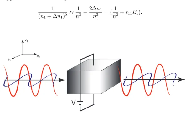
described by the following equation, ( 1 n2 1 + r11E1)x21+ ( 1 n2 2 + r21E1)x22+ 2r61E1x1x2 = 0.
CHAPTER 2. ELECTRO-OPTIC MEDIA 8
Since the term containing r61 is responsible for the refractive index change in the
x1 direction, we can ignore this term for a moment.
1 (n1+ ∆n1)2 = (1 n2 1 + r11E1),
For the electric fields lower than 20 kV/cm, O[∆n] ≈ 10−4 so ∆n
1 & n1. For
this approximation we can expand the formula as 1 (n1+ ∆n1)2 ≈ 1 n2 1 − 2∆n1 n3 1 = (1 n2 1 + r11E1).
V
x1 x2 x3Figure 2.1: Basic illustration of an passing light though the electro-optic medium which is modulated by an external voltage.
The corresponding index change along the x1 direction is,
∆n1 ≈ −
n3 1r11E1
2 .
Making the same assumption we can get the index change along x2 direction as,
∆n2 ≈ −
n3 2r21E1
2 .
A polarized light wave propagating along the x3 direction can be decomposed into
two component: one along the x2 direction and the other along the x1 direction.
We can define these waves as follows
CHAPTER 2. ELECTRO-OPTIC MEDIA 9
k0 is the wave number in free space. When the light covers a distance L in the
electro-optic medium, a relative phase shift is observed between these orthogo-nal polarized components and this shift depends on ni(i = 1 or 2). After the
propagation with a distance L in the x3 direction in the crystal, the phase shift
is, ∆φ1 =−k0L [n2− (n2 + ∆n2)] = − k0n32r21E1L 2 , ∆φ2 =−k0L [n1− (n1 + ∆n1)] = − k0n31r11E1L 2 .
This calculation is done for the steady electric field. For the sinusoidally varying time dependent electric field E1, the phase shift between these components also
vary sinusoidally. As a result phase modulation will occur [15].
2.3
Kerr Effect
In 1876 John Kerr (1824-1907) stated that under the influence of the electric field, isotropic materials show uniaxial behaviour. The uniaxial materials show two different refractive indices for the propagation direction (extraordinary index ne)
and normal to the propagation direction (ordinary index no). As a result of this
index difference for these directions, a birefringence is observed. This phenomena is named as the Kerr effect. This effect is distinguished from the preceding Pockels effect with a quadratic electric field dependence [15]. Impermeability tensor (1/n2) is defined as the the inverse dielectric constant. The changes in the
refractive index according to the applied electric field is evaluated by using the 6× 6 impermeability tensor ρ. To simplify the calculations, we use a coordinate system along the principal axes. So all the terms of the tensor become zero except the diagonal terms
ρ11= ρ22= ρ33 = ρ.
The applied electric field is in the z direction E1 = E2 = 0, E3 = E. The refractive
CHAPTER 2. ELECTRO-OPTIC MEDIA 10
isotropic medium n is defined as 1 n2 " = 1 n2 e = 1 n2 + ρE 2.
Since the electric field is applied in one direction, the refractive index of the ordinary axis does not change and remains the same
1 n2 ⊥ = 1 n2 o = 1 n2.
As a result, the presence of the electric field changes the property of the isotropic medium and the medium shows uniaxial crystal behaviour with an optical axis parallel to the electric field. Again we assume that the change in the refractive index n0 is small compared to ne, so that we can use the binomial expansion to
write 1 n2 e = 1 (n0+ ∆n0)2 = 1 n2 0 − 2∆n0 n3 0 = 1 n2 0 + ρE2.
Refractive index difference between the ordinary and extraordinary axes can be measured by means of the induced birefringence and it is experimentally expressed as
∆n = KE2λ,
where K is called the Kerr constant. When the polarized light passes through the Kerr medium a phase difference between the ordinary and extraordinary axes occurs which is formulated as
Γ = 2π∆nL
λ = 2πKE
2L.
By putting k0 and ∆n instead of 2πλ and (ne− no), we can reformulate the above
expression. Γ = k0(ne− n0)L = k0(n0 + ∆n0− n0)L = 2π λ ∆n0L = π λn 3 0ρE2.
CHAPTER 2. ELECTRO-OPTIC MEDIA 11
By matching the theoretical and experimental expressions we can extract the Kerr constant as
K = n
3 0ρ
2λ .
As a special case, to get a phase shift of Γ = π for a medium with thickness d and length L half wave voltage is defined [15] as
Vλ 2 = d √ 2KL.
Electro-Absorption Effects
Absorption of the incident light near the band gap of the photonic material has a significant advantage to modulate the light. By externally applied electric field, the absorption characteristics of both bulk semiconductors and multi quantum well structures (MQW) can be changed. These modifications of the absorption spectra due to electric field also effect the refractive index of the material through the Kramers-Kronig relation. Also the interaction of the electrons and holes with the optical field contributes the refractive index change named as the plasma contribution. According to the Drude model, the change in the carrier population induce the refractive index change as follows,
∆n≈ −Nxe
2λ2
8π2&
0nc2m∗x
,
where Nx and m∗x are the excitonic (i.e., electron-hole) concentration and the
excitonic effective masses, respectively [17]. Empirically, for a density of 1019
cm−3 in electron-hole doping for fused silica at a wavelength 1.55 µm, we are
expecting a change in the refractive index ∆n ∼ 0.0149. The refractive index of fused-silica for the given wavelength is n = 1.444. So plasma effect has a non-negligible of a per cent contribution to the refractive index change.
CHAPTER 2. ELECTRO-OPTIC MEDIA 12
2.4
Quantum Confined Stark Effect
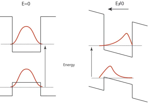
As it is known, the applied electric field causes a change in both wave function and energy state of the quantum systems. The perturbation theory predicts a shift in the ground energy called Stark effect that triggers the excitation of the electrons from valence band to the conduction band. The quantum structures
E=0 E=0
Energy
Figure 2.2: In the presence of the electric field, band gap of the material is reduced which enables in tunnelling of the electron to the conduction band.
involve alternating layers of GaAs and AlGaAs with a thickness of the order of 100 nm. These layers form the quantum wells where each well shows quantum mechanical size effects. Applied electric field perturbs the states and pushes them to get closer. As a result the exciton resonances shift to lower photon energies, in other words longer wavelengths, hence introduces a red shift. This red shift results with the new absorption peaks associated with the formation of the exciton and enables forbidden transitions. In these structures, the separation of the excited electron with the hole is expected to be larger than the thickness of the layer, however the thin well walls of the structure impose a constrain to the exciton structures to bring them closer.
CHAPTER 2. ELECTRO-OPTIC MEDIA 13
This constrain restrict the movement of the exciton and this restriction is called quantum confinement. The benefit of the confinement systems is the asso-ciated absorption peaks which would otherwise not be easily observed in the bulk systems [18]. Although the electric field brings the states closer, it applies force on electrons and holes in opposite directions which weakens the binding of the exciton. But we can still observe well defined excitonic states. Compared to the bulk systems, under such higher electric fields, exciton resonances can be remain in the confinement systems without excessive broadening [27]. By choosing the appropriate frequency of the light for the applied electric field, the absorption of the electro-optic medium can be changed which is the basis of an optical modula-tor [18]. The application of this effect to the bulk systems can be questioned. The following reason may answer this question. The contribution of the electric field is taken as a perturbation to the solution of the eigenstates of the system. To get significant shift in the eigenstates of the system, the electric field energy eEaB
in terms of the effective Bohr radius, electron charge and electric field should be comparable with the absorption edge energy, eEaB ≥ ∆. This equation needs
a field of the order of 106 V/m for different material parameters. However such
strong fields of this order broaden even destroy the exciton resonances. One of the reason beside this broadening is the field ionization of the exciton, penetration of the electron through the finite Coulomb barrier at finite fields. The other reason is the impact ionization. Free carriers in the medium can gain high energies in the presence of electric field. The hitting of this high energetic carriers to the exciton may result with ionization of the exciton or broadening of the excitonic resonance [19]. By confining the electron-hole system, one can overcome this problem for the following reasons:
• since the electrons and holes have opposite electric charges, in the presence of the electric field they feel repulsive electric force. This force pushes them to opposite sides of the layers that reduce the energy of the electron-hole pair resulting with a red shift.
• the walls of the quantum well prevent the electron and hole from tunnelling out of the layers. For the strong confinement, it is important that, the well width should be narrow compared to the exciton size [27].
CHAPTER 2. ELECTRO-OPTIC MEDIA 14
Stark effect modifies the excitonic resonances and this modification yields change in the refractive index through the Kramers-Kronig relation. As a result we can achieve Pockels or Kerr like effect to modulate the light.
2.5
Franz-Keldysh Effect
In the previous section, the effect of the applied electric field on the quantum systems is expressed as Stark effect. Reduction of the band gap by the Stark effect results in the increasing excitation of the electrons to the conduction band with the energy ¯hω < Eg. However this work for the quantum confined systems.
Because, if the applied field exceeds the classical ionization energy of the order of a few times, exciton resonance broadens as a result of ionization [27] as men-tioned in the previous section. For the bulk semiconductors, Franz and Keldysh independently proposed another effect of the electric field. The applied field re-sults in an exponential tail of the wave functions into the forbidden zone of the semiconductor, and over this tail electrons can tunnel to the conduction band from the valence band absorbing a photon with a energy ¯hω < Eg [29]. As a
result, overlap between the hole and electron wave functions leads the transition for the energies smaller than Eg. As the electric field increases, the exponential
tail and amplitudes of the Franz-Keldysh oscillation increases [28].
Fascinating property of the Franz-Keldysh effect is that it renders a single semiconductor to have an tunable ”band gap”. Recall that Stark effect is observed in quantum wells which requires expensive fabrication techniques. In contrast to the Stark effect, Franz-Keldysh effect lets us use bulk semiconductors which has a simple growth procedure covering a wide range of the wavelengths. Also insensitivity to the high optical powers make this approach stable. Powers higher than 250 W/cm2 saturates the Stark effect, on the other hand the Franz-Keldysh
effect remains unperturbed up to powers of 20 kW/cm2. Above this power an
other optical effect named band filling contributes. Response time of the electro-optic devices are limited by the low saturation intensity which means that higher intensity results with higher response speed. For the optical modulators this
CHAPTER 2. ELECTRO-OPTIC MEDIA 15
property becomes important for the following reasons:
• optical power as low as mW can saturate the excitons which will diminish the Stark effect,
• to modulate the light by using the Stark effect we need polarization pre-serving waveguides.
Although it seems that the usage of the Franz-Keldysh effect is advantageous compared to the Stark effect, huge power need of the system must also be con-sidered [20].
2.6
Quantum Confined Pockels Effect
For the case of quantum wells, if the barrier and well materials share common ion such as InxGa1−xAs-InP at interfaces, the sample shows optically isotropic
medium in the plane perpendicular to the growth direction. Under applied electric field, this rotational symmetry at the interface is broken and a strong enhance-ment of quantum confined Pockel effect is observed. Theoretical background of this symmetry breakdown can be understood by adding an interface term to the valence band Hamiltonian. This term is invariant of the C2v group and can be
treated as a perturbation in the framework of the classical envelope-function the-ory. In other words, because of this perturbation, heavy and light hole states are mixed as a function of applied field at the minizone, and this mixing breaks the in-plane isotropy [22].
2.7
Burstein-Moss Effect
In 1953, Tanenbaum and Briggs tried to explain the different band gap mea-surements of indium antimonide (InSb) for different temperatures. There are divergent band gap values with the increasing temperature and they concluded
CHAPTER 2. ELECTRO-OPTIC MEDIA 16
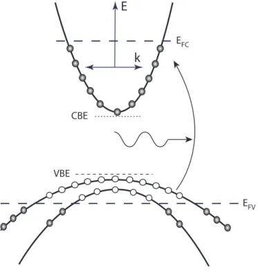
that this results from impurity effects [1]. However this anomalous change in the absorption edge is explained differently in the same year by Burstein and Moss independently. They proposed that the explanation of this absorption limit is based on the small effective mass of electrons rather than impurity effect. Since the bottom of the conduction band of InSb has sharp curvature and at this region there exists small density of states. This density of states results with small effec-tive mass of electrons. As the carrier density increases the difference between the Fermi energy level EF and the conduction band edge increases rapidly since the
electrons fill the small available states in the conduction band [2]. For the case of
E
k
CBE VBE EFC EFVFigure 2.3: As the carrier densities increase in both valence band and conduction band, excitation of an electron to the conduction band requires more energy. n-type doping, the electron contribution to the conduction band comes from two different type of sources. One of the sources is the electrical injection of donors to the semiconductor. The thermal ionization of the donors introduces electrons to the conduction band. The other means is by photo-injection excitation of an electron from valence band to the conduction band, absorbing a photon. As the free carrier concentration increases in the medium they fill the available states
CHAPTER 2. ELECTRO-OPTIC MEDIA 17
at the bottom of the conduction band. So the excitation of an electron over the Fermi level of the conduction band while conserving its momentum (with the same k value) requires much more energy compared to the band gap Eg of the
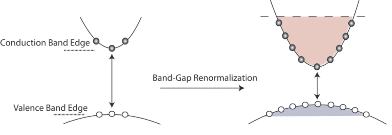
intrinsic semiconductor as shown in Fig. 2.3 However, due to the many body effects, for high densities, band gap narrowing effect can be also observed [23] as stated in the following Fig. 2.4. More about the band gap renormalization will be given in the following chapters.
Band-Gap Renormalization Conduction Band Edge
Valence Band Edge
Figure 2.4: As the carrier densities increase in both valence band and conduction band, due to the many body effects band gap is renormalized.
2.8
Purcell Effect
Finally, we would like to discuss an effect which is not an optic or electro-absorption effect, but nevertheless it has recently attracted strong interest in a similar context. The main physical idea in this effect is the control of the spon-taneous emission. One of the main phenomena for the creation of light is sponta-neous emission. In the presence of stimulated emission, spontasponta-neous emission can be somehow troublesome. Since it can limit the performance of photonic devices such as lasers, displays, illuminations and so on. For lasers, stimulated light is coherent, however spontaneous emission (SE) does not contribute to lasing. Since it does not couple with the laser beam it emerges as noise that is an unwanted
CHAPTER 2. ELECTRO-OPTIC MEDIA 18
situation that scientists want to get rid of. Also for the case of the LEDs, the problem emerges in a different way. Basic working principle of the LEDs is based on the SE. However, the problem lies under this idea is the only limited ratio of the light extracted from the device and most of the light is confined inside the semiconductor. For different situations there are different motivations to inhibit the SE or to increase the efficiency of SE [24].
By using a cavity, Purcell suggested a method to control the SE rate. Usage of a cavity leads to a modification of dipole-photon coupling and available pho-ton modes allow us to fabricate high efficiency LEDs also let us to inhibit the undesired wavelengths [25].
Now let us first analyse the the working principle of Purcell effect. An emitter with a wavelength λe, linewidth ∆λe placed in a resonance which has a single
mode with a wavelength λc, linewidth ∆λc and a quality factor Q = λc/∆λc.
Since λe& ∆λc, the time need for photon to leave the cavity is much shorter than
the radiative lifetime. So the re-absorption of the emitted light is now negligible which can be defined as weak coupling regime. Different from the vacuum the emitter feels a quasi-continuum of modes. By using the Fermi golden rule, the rate of spontaneous emission is written as
1 τ = 4π ¯h ρcav(ω " |(d· (&(r)|2#,
where (&(r) is the vacuum electric-field vector at the location (r) of the emitter and (d is the electric dipole, ρcav(ω) is the density of modes of the cavity at the
emitters frequency. SE rate in the cavity mode, compared to the total SE rate in a medium, is given by the Purcell factor
Fp =
3Qλ3 c
4π2n3V ,
where n is the refractive index of the medium, Q is the quality factor of the cavity and V is the volume of the cavity [26]. As a result, the cavity increase the spontaneous emission of the dipole by tuning the frequency of the emitter.
Chapter 3
The Relevance of This Work to
Semiconductor Lasers
On 6 August 1960, Theodere Mainman published a paper in Nature, about the first working laser developed at the Hughes Research Laboratory in California [46]. He pumped silver coated ruby rod with high power flash lamp and the laser produced a short of flash light. This marked the initiation of a research area which turns into a billion dollars worth of industry. By the development of different types of laser such as semiconductor lasers, solid state lasers, gas lasers, etc, lasers inevitably became part of our lives. If we take into account the economic impacts of the lasers, the semiconductor lasers stand out. They are now widely used in areas such as CD players, laser printers, military and bio-medical applications. Continuously improvement in the performance of the semiconductor lasers such as low-threshold current, high speed direct current modulation, ultra-short optical pulse generation, high optical output power, low cost and etc. is the main reason behind this major surge [47].
CHAPTER 3. SEMICONDUCTOR LASERS 20
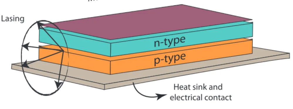
3.1
Basic Structure
The working principle of a semiconductor laser basically depends on the recom-bination of the carriers injected from the p− n junction. Basic schematic of an semiconductor laser is shown in Fig. 3.1. When we forward bias the junction, electrons are injected from the n-type doped layer and holes are injected from the p-type doped layer to the intrinsic (active) region. After the accumulation of the electrons and the holes in the active region (pumping), electrons and holes are stimulated to recombine in the active region. Each stimulated electron-hole recombination results in the emission of a coherent light to the optical field.
n-type
p-type
Heat sink and electrical contact
Metal contact
Lasing
Figure 3.1: Basic structure for the semiconductor laser.
3.2
Photoexcitation and Attainment of
Quasi-Equilibrium
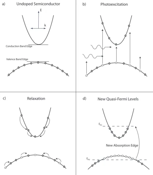
The primary purpose of this thesis is to study the refractive index change due to equal concentration of electron and holes (n = p). This can be achieved by
CHAPTER 3. SEMICONDUCTOR LASERS 21
the basic p-n junction drawn in Fig. 3.1 through electrical injection. However,
k E
Conduction Band Edge
Valence Band Edge
Photoexcitation Relaxation a) b) c) Undoped Semiconductor EFC EFV
New Absorption Edge New Quasi-Fermi Levels d)
Figure 3.2: Photoexcitation in semiconductor lasers.
in the case of InN, its p-doping is a major challenge. For this reason, we shall consider optical injection of equal number of electron and holes. In Fig. 3.2(b) we show the electron hole generation under a broadband illumination with an energy highly above the band gap of InN. The carriers then quickly relax to band edges Fig. 3.2(c) by emitting optical phonons. This results in the attainment of a new quasi-equilibrium of the excited carriers (see Fig. 3.2(d)). It should be noted that these electron-hole pairs will radiatively recombine in a duration of nanoseconds and this non-equilibrium population will be lost. For this reason the
CHAPTER 3. SEMICONDUCTOR LASERS 22
optical pumping process needs to be kept on, in order to preserve a steady-state quasi-equilibrium carrier distribution.
3.3
Carrier Distribution
This quasi-equilibrium carrier distribution corresponds to the population inver-sion which is required so as to amplify an optical radiation of a frequency ν. The quasi-Fermi energy difference between the electrons and the holes determines the photon energy. Note that, under equilibrium, Fermi levels of electrons EF c and
Fermi level for the holes EF v equal to the Fermi level of the whole system
EF c = FF v = EF.
However, under optical or electrical injection, the system is driven into non-equilibrium state. The Fermi levels of the electrons and the holes split and construct the new quasi Fermi levels of the systems. Under non-equilibrium conditions, the electron concentration n and the hole concentration p are given as n = Ncexp $ −Ec − EF c kBT % , p = Nvexp $ −EF vk− Ev BT % .
Here, under parabolic band assumption the effective density of states for the electrons Nc and that for the holes Nv are written as,
Nc = 2 & 2πm∗ ekBT h2 '3/2 , Nv = 2 & 2πm∗hkBT h2 '3/2 ,
where kB is the Boltzmann constant and h is Planck’s constant.
The new quasi-Fermi levels become, EF c = Ec + kBT ln
$ n
Nc
% ,
CHAPTER 3. SEMICONDUCTOR LASERS 23 EF v = Ev− kBT ln $ p Nv % ,
where Ec is the bottom energy level of the conduction band and Ev is the top of
the valence band.
The distribution function for the electrons having energy E1 in the valence
band is f1 and for the electrons having energy E2 in the conduction band is f2.
By using the quasi-Fermi levels EF c and EF v, we can write f1 and f2 as
f1 = 1 exp [(E1− EF v)/kBT ] + 1 , f2 = 1 exp [(E2− EF c)/kBT ] + 1 .
f1 is given for the occupation of electrons for the valence bands, so the hole
distribution function in the valence band is given by [1-f1] [49].
3.4
Chirp
Up to this point, we assume that the semiconductor laser is very stable and lases at a single mode. However, during population inversion, the accumulation of electrons and holes in the active region changes the absorption coefficient of the semiconductor. Also the new carrier population renormalizes the band gap.
When an electromagnetic pulse propagates through a medium, the bound electrons of the dielectric display a wavelength dependent response. In general, the refractive index of the material varies as
1 < nred(λ) < nyellow(λ) < nblue(λ).
The variation of the refractive index results in different group velocities of each spectral component as
vg(λ) =
c nλ
,
where c is the speed of light. This phenomenon is named as dispersion. Longer wavelength component of the pulse has larger group velocity, therefore leading part of the pulse has low frequency which is called red shifted. However, if the
CHAPTER 3. SEMICONDUCTOR LASERS 24
medium has an anomalously dispersive property so that refractive index changes as
1 < nblue(λ) < nyellow(λ) < nred(λ),
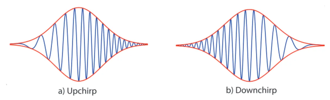
the leading part of the pulse is now high frequency components which is called blue shifted. As a result of the dispersion, the instantaneous frequency of the pulse changes and this change is called chirp. Also nonlinearities in the medium causes chirp on the pulse. Besides, dispersion and nonlinearities, in semicon-ductor lasers refractive index change depending on electron and hole population leads to a chirp which is the main subject matter of this thesis. In this context, we can distinguish between two different types of chirp. If the instantaneous frequency has an increasing function, we call it up-chirped pulse. Fig. 3.3 shows the difference of these types of chirp. In this type, the leading part of the pulse is blue shifted. On the other hand, if the pulse has time dependent decreasing instantaneous frequency, it is called down-chirped pulse and the leading part of the pulse is red shifted. The chirp on the pulse can be removed by propagating the wave in a suitable dispersive medium.
a) Upchirp b) Downchirp
Figure 3.3: (a) shows the up-chirp with increasing instantaneous frequency, (b) shows the down-chirp with decreasing instantaneous frequency.
Chapter 4
Further Technical Preliminaries
In this chapter, we provide in depth information on three technical issues which will be of importance in the rest of the thesis. These are the tetrahedron inte-gration technique by Lehmann Taut and the discussion of Van Hove singularities in bulk semiconductors. The common denominator of the both subjects is that they both take place in the reciprocal lattice. Finally, we provide some theoretical information on the Kramers-Kronig relations.
4.1
Brillouin-Zone Integrations
Quite commonly in solid state calculations, one ends up with an integration over a surface (usually Fermi surface), as in density of states, effective mass tensor or response functions. Conventional integration routines for calculating the density of states and similar kind of integral types in the form
( dS
|grad∆ε(k)|A(k),
encounter serious complications. In an energy interval, D(ε) is inversely propor-tional to the square root of the mesh points and increasing in the mesh point leads to increase of statistical noise. As a result, Gilat and Raubenheimer propose a
CHAPTER 4. FURTHER TECHNICAL PRELIMINARIES 26
different integration routine to solve this problem [40]. They divided whole Bril-lioun zone into cubes with the same volume. All the reciprocal space is reached by linear extrapolation of the cube centers. The integration over the constant energy or frequency surface is now replaced by the cross sections of small areas between the cubes and the constant surfaces. On the other hand, Lipton and Jacobs modified this method, and they interpolated the energy points between the corners of the cubes that reduces the computational load [41]. However, both of these methods cannot fill the boundary of the reciprocal spaces so these boundaries need to be coded explicitly.
4.1.1
Lehmann-Taut Method
Lehmann and Taut approached to the problem in a different way and they divided reciprocal lattice into tetrahedra, as the whole Brillioun zone can be totally divided into tetrahedra including the boundaries [42]; see Fig. 4.1.
kz ∆ kx ∆ ky ∆
Figure 4.1: Filling of Brillioun zone with tetrahedra.
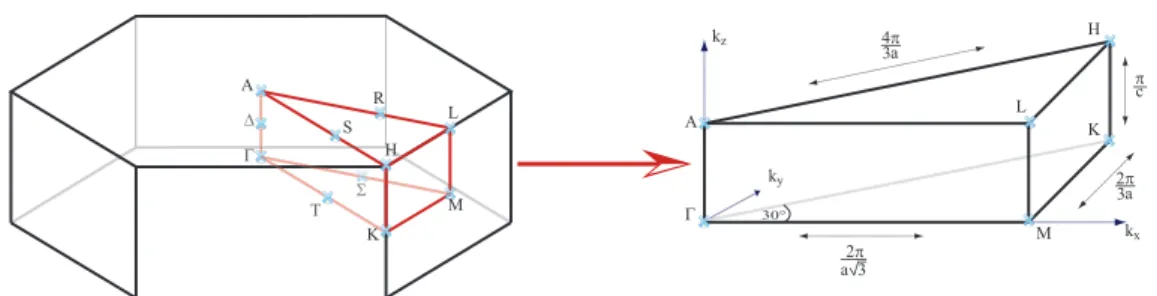
Wurtzite InN has hexagonal reciprocal structure. Any volume integration over this Brillioun zone can be reduced to irreducible Brillioun zone (IBZ) by using the all symmetries of the lattice as shown in Fig 4.2.
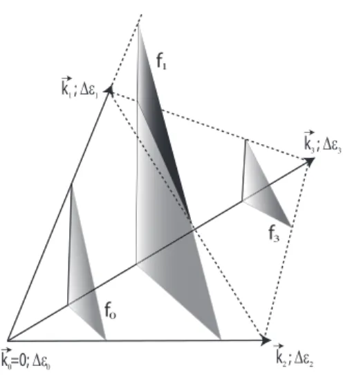
Then the IBZ is divided into a mesh of 40×40×40 in both basal plane and along the z axis shown in Fig. 4.3 and every mesh is then divided into tetrahedra. Let the energy value at k0 = 0 corner of the tetrahedron be ∆ε0and for the corners
ki(i = 1, 2, 3) be denoted as ∆εi, respectively. Within the tetrahedron, the energy
values ∆ε(k) can be determined by linear interpolation as ∆ε(k) = ∆ε0+ b· k.
CHAPTER 4. FURTHER TECHNICAL PRELIMINARIES 27 Α ∆ Γ R L H S T K M Σ H H H H H H 30° Γ Α M K H L kz kx ky 2π π c 4π a 3 2π a 3 3 a
Figure 4.2: First Brillioun zone of the wurtzite lattice and its IBZ b is determined by these series of formulas,
rj· ki= δij; r1 = k2× k3 v ; r2= k3× k1 v ; r1 = k1× k2 v , and b = 3 ! i=1 (∆εi− ε0) ri
where v is the six times tetrahedron volume. Also the function A(k) is interpo-lated in a similar way as
a(k) = a0+ a· k.
Now we knit the any kind of the integrand as a spider’s net.
30° kz kx ky 2π π c 4π a 3 2π a 3 3 a ∆ kz ∆ ky ∆ kx
CHAPTER 4. FURTHER TECHNICAL PRELIMINARIES 28
4.1.2
Application to Density of States
The density of states is given by the expression, g(E) =
( dS
grad∆ε(k),
dS represents the surface integral over the volume. By a simple derivative, the denominator turns into form
grad∆ε(k) = grad(∆ε0+ b· k) = k,
since grad∆ε0 = 0. The contribution of one tetrahedron to the density of states
is calculated with an energy ∆ε(k) = ε is i0(ε) =
(
∆ε(k)=ε
dS b ,
and this integral representation turns into simple mathematics calculation such as
i0(ε) = f (ε).|b|−1.
f (ε) is the intersection of the constant energy surface with the tetrahedron and these cross sections shown in Fig. 4.4 can be written as the sum of the triangular areas [42]. f (ε) = f0 ∆ε0 ≤ ∆ε ≤ ∆ε1 f0− f1 for ∆ε1 ≤ ∆ε ≤ ∆ε2 f3 ∆ε2 ≤ ∆ε ≤ ∆ε3
where the integrands come out as,
f0|b|−1 = v2 (ε−∆ε0) 2 (∆ε1−∆ε0)(∆ε2−∆ε0)(∆ε3−∆ε0) f1|b|−1 = v2 (ε−∆ε1) 2 (∆ε1−∆ε0)(∆ε2−∆ε0)(∆ε3−∆ε0) f3|b|−1 = v2 (ε−∆ε3) 2 (∆ε1−∆ε0)(∆ε2−∆ε0)(∆ε3−∆ε0).
CHAPTER 4. FURTHER TECHNICAL PRELIMINARIES 29 k =0; ∆ε0 0 k ; ∆ε1 1 k ; ∆ε2 2 k ; ∆ε3 3 f0 f1 f3
Figure 4.4: Different intersections of a tetrahedron with three different constant energy surfaces.
4.1.3
Effective Mass and Dielectric Tensors
In this thesis we need the energy-dependent effective masses. To obtain the m∗(E), we can define the group velocity of the carrier as
v = 1 ¯h∇kE.
By taking the derivative of the velocity, we get the acceleration,
a = dv dt = 1 ¯ h d dt∇kE = 1¯h∇k -∇kE· dkdt . .
The acceleration of the free carrier is a result of an external field F and time dependent wave solution of the carrier requires
F =−¯h(dk/dt). When we substitute F into the a and from F = m∗a,
a = −1
¯h2∇k∇kE · F, m∗ = ¯h
2
CHAPTER 4. FURTHER TECHNICAL PRELIMINARIES 30
we get the energy-dependent effective mass of the carrier [43].
Just like the density of states and energy-dependent effective mass tensor calculations, we can obtain the imaginary part of the dielectric function using the tetrahedron integration technique [50]. The corresponding expression is given by
Im/&ab(ω)0= e 2 π ! v,c ( BZdk r a vc(k)rbvc(k)ravc(k)δ (Ec(k)− Ev(k)− ¯hω) .
4.2
Van Hove Singularities
We have shown the calculation method of density of states by using Lehmann-Taut method for the type of integral
gn(ε) = ( S(ε) dS ∇kεn(k) ,
which reconciles the density states with the band structure of the semiconductor. More detailed work is shown in the preceding chapters. At this point, we prefer to focus on the mathematical meaning. The S(ε) represents a constant energy surface. If we use for the energy, that of the energy difference between bands n and n% as in
εn(k)− εn!(k) = ε0,
and similarly for the gradient
∇ [εn(k)− εn!(k)] = 0,
what we obtain is called joint density of states since it gives the density of pair of states: one is empty, the other one is occupied with an energy difference ε0.
Hence the joint density of states is represented as [44] Jnn! =
(
εn(k)−εn!(k)=ε0
dS
∇ [εn(k)− εn!(k)].
The singularities in the integrand are known as Van Hove singularities and oc-cur when the constant energy surface contains the band points whose gradient vanishes. However, these singularities are integrable and yields finite values and contribute to the density of states and the slope of the density of states at these
CHAPTER 4. FURTHER TECHNICAL PRELIMINARIES 31
Van Hove singularities
Densit
y of Stat
es
Energy
Figure 4.5: Different types of van Hove singularities. The arrows indicate the energies where the singularities exist. The circles shows the discontinuities in the derivative of the density of states .
point diverges [45]. A basic schematic of these singularities in the density of states is shown in Fig. 4.5.
We can encounter these singularities when, ∇kεn(k) =∇kεn!(k) = 0,
or more generally for
∇k[εn(k)− εn!(k)] = 0.
The first condition occur at the high symmetry points and the second condition may occur at any k vector [44].
Now lets go back the physical meaning and importance of these singulari-ties. For the direct transitions between bands n and n% which are parallel at a particular k values with an energy difference εnn!, a different density of states is
responsible [52]. At these points during measurement of the optical properties of semiconductor, a peak is expected. For our cases, computation of the absorption of the medium for the photons with an energy ¯hωnn! = εnn! we are also expecting
CHAPTER 4. FURTHER TECHNICAL PRELIMINARIES 32
peaks in the corresponding energies of these singularities. For the calculation of the imaginary part of the dielectric function at these energies and in their neigh-bourhood, van Hove singularities dominate the absorption characteristics of the semiconductor.
4.3
Kramers-Kronig Relation
As a main idea of this chapter we almost gave the technical procedure for our computational work. As a final step we need to calculate the imaginary and real part of the dielectric function to conclude the refractive index change for the InN. Imaginary part of the dielectric function is responsible for the absorption of the medium and again is stated by the following formula
Im/&ab(ω)0= e 2 π ! v,c ( BZdk r a vc(k)rbvc(k)ravc(k)δ (Ec(k)− Ev(k)− ¯hω) .
To compute the real part of the function by using the imaginary part we use the causality principle and the mathematical procedure is given by the Kramers-Kronig relation. So at this point it is necessary to open a parenthesis to discuss the Kramers-Kronig relations. These details are taken from the reference [52]. These relations have great importance since they allow us to evaluate the components of the dielectric function, conductivity, susceptibility or other optical properties of the semiconductor, if we know the one of reflection or absorption of the medium. By involving the causality, derivation between the complex and real part of the response function can be done. To describe the linear response ˆX of the system for an arbitrary time t and a position r to a external perturbation in terms of an external stimulus ˆf at a time t% and location r% we use the following formula
ˆ X(r), t = ( ( ∞ ∞ ˆ G(r, r%, t, t%) ˆf (r%, t%)dr%dt%,
where ˆG(r, r%, t, t%) is the response function. By using the Cauchy’s theorem and
causality we get the relation ˆ G = 1 iπP ( ∞ ∞ ˆ G(ω%) ω%− ωdω %.
CHAPTER 4. FURTHER TECHNICAL PRELIMINARIES 33
When we divide ˆG into real and imaginary parts as ˆ
G = G1(ω) + iG2(ω),
and this leads the following relations between the real and imaginary parts of ˆG G1(ω) = 1 πP ( ∞ ∞ G2(ω%) ω%− ω, G2(ω) =− 1 πP ( ∞ ∞ G1(ω%) ω%− ω.
For the real part of the dielectric function, the expression is stated in Gaussian units as Re{&(ω)} = 1 + 2 πP ( ∞ 0 ω%Im{&(ω%)} ω%2− ω2 dω %.
More information and intermediate steps can be found in the relevant chapter of the Ref. [52].
Chapter 5
Band Gap Renormalization
Since the invention of the first semiconductor laser, the understanding of the density dependent optical spectra has attracted attention. Especially many-body effects of highly dense carriers such as exchange and correlation energy in the material renormalize the band gap and also affect other optical properties such as refractive index and the overall optical susceptibility. The spin distribution of the carriers ultimately affect the charge distribution of the system. Pauli principle excludes the same spin electrons or holes to be in the same position at the same time. As a result, electrostatic energy of the system will be reduced according to the redistribution of the carriers and the energy difference compared to noninteracting uniformly distributed carriers is called exchange energy [30]. However, this energy deviates from the exact non-relativistic energy of the system. The difference between these energy is called correlation energy. This Hartree-Fock energy is an upper bound limit to the non-relativistic exact energy of the system, which means that the correlation energy is always negative [31].
Increasing in the carrier population strongly influences the Coulomb interac-tion between the electron-hole (e-h) pairs. In the plasmas, one emerging property is the screening of the Coulomb potential, and the (e-h) plasma screening of the Coulomb interaction is given by,
Vs(q, w) = Vq/ε(q, w),
CHAPTER 5. BAND GAP RENORMALIZATION 35
where Vq is the unscreened Coulomb potential and the ε(q, w) is the longitudinal
dielectric function. The dielectric function is usually approximated by Lindhard formula [33]. ε(q, w) = 1− Vq 1 V ! i=e,h;k fi,k− fi,k+q ¯hω + iδ− εi,k+q ,
where εi,k and fi,k are the e-h energies and distribution functions respectively.
The subscripts i and k refer to the band index and wave vectors respectively. If the carriers are in the equilibrium state, the distribution function is given by the Fermi distribution
fi,k=
1
exp [(εi,k− µi)β] + 1
, where µi is the chemical potential, β = 1/kbT .
5.1
Plasmon-Pole Approximation
In 1989 Haug and Koch simplified the Coulomb self-energy calculation by using the so called plasmon-pole approximation [32]. By using static plasmon-pole approximation, Lindhard formulation turns into the following simple form,
1 &q = 1 1− ω 2 pl ω2 q 2 ,
where ωq is the dispersion of the effective plasmon mode and for 3D systems. The
governing formulas can be written as Vq = 4πe 2 $0q2, ω2 pl = 4πe 2n $0µx = -E0 ¯ h .2 , ω2 q = ω2pl -1 + κq22 . + C 4 -¯hq2 2µx .2 ,
where µx is the reduced e− h mass µx = memh/(me + mh), n is the plasma
density, C is a numerical constant, E0 is the Rydberg constant and κ is the
inverse screening length, which can be obtained by the formula κ2 = 4πe 2 &0 ! i ∂n ∂µi .
CHAPTER 5. BAND GAP RENORMALIZATION 36
The band gap of the material shrinks with the increasing carrier population due to the many-body exchange and correlation effects. The corresponding the band gap shift is given by
∆Eg = [Vs(r = 0)− V (r = 0)] − V1 3qVs(q)(fe,q + fh,q),
= ∆EgCH+ ∆EgSX,
where ∆EgSX screened exchange correlation and ∆EgCH is the Coulomb hole
contribution. For 3D, ∆EgCH, Coulomb hole contribution is given by
∆EgCH =− 2E0a0κ -1 + C1/2- E0 ¯ hωpl . (a0κ)2 .1/2.
The screened exchange term is integrated numerically. However, there does not exist a recipe for the value of numerical constant C for an arbitrary material. This reduces the applicability of this approximation for in general materials.
5.2
Vashishta-Kalia Model
Vashishta and Kalia (VK model) simplified the exchange and correlation energy for p-n type materials and showed that the band gap renormalization is indepen-dent of the band characteristics [34]. However, further studies showed that in wide-gap semiconductors such as II-VI group elements, VK model deviates from experimental results [35].
Vashishta and Kalia simply fitted [34] the exchange and the correlation energy of the semiconductors to the expression
εxc= a + brs c + drs+ r2s , where a =−4.8316, b =−5.0879, c = 0.0152, d = 3.0426.
CHAPTER 5. BAND GAP RENORMALIZATION 37
rs is the dimensionless inter-particle distance, which is defined in terms of carrier
density n, static dielectric constant ε and effective bohr radius a∗
B = ¯h2ε/µe2 4π 3 (a ∗ Brs)3 = 1 n.
What we expect is that VK model would fit to the recent experimental data
-0.6 -0.5 -0.4 -0.3 -0.2 -0.1 0 1018 1019 1020 1021 Band-Gap Renormal izat ion (eV) Carrier density (cm ) RPA VK Exp -3
Figure 5.1: The dashed lines are the VK formulation for the band gap renormal-ization. Solid lines are the formulation of Sernelius approach. The symbol points are taken from the experimental data in Ref. [36].
for GaN since GaN is an III-V group compound as InN. It was experimentally shown that for GaN the band gap renormalization is temperature (T ) independent [36]. This independency makes GaN a good sample to check the validity of the VK model up to plasma densities for an arbitrary temperature. For GaN we calculated the density dependent effective masses for both holes and electrons. As static dielectric constant, 9.5 is used. According to the VK model we get ∆EBGR of GaN as a function of e− h density, n between a range of 1×10¹⁸ and
1×10²¹ as shown in Fig. 5.1. When we compare our calculation with the data
taken from Ref. [36], we observe that VK model deviates from the experimental data significantly. For further calculations such as the refractive index, VK model loses its validity at this range of the carrier density for our purposes.
CHAPTER 5. BAND GAP RENORMALIZATION 38
5.3
Random Phase Approximation
For heavily doped n-type materials, the electron-electron and electron-ion con-tributions are well estimated by the random phase approximation (RPA). The contributions are defined by the following formulas
∆Ec−c =− 2e2k F π&0 − e2k T F 2&0 1 1− 4 πarctan & kF kT F '2 , ∆Ec−i =− 4πe2n &0a∗BkT F3 ,
where n is the carrier density, &0 is the static dielectric constant,
kF =
4
3π2n51/3, is the Fermi wave number,
kT F = 2
6
kF/(πa∗B),
is the Thomas-Fermi wave number, a∗
B is the effective bohr radius, which uses m∗e
for the conduction band effective carrier mass. For n-p type of GaN, we modified the effective carrier mass into reduced effective e-h masses µx. It is first seen in
Fig. 5.1 that the deviation of n-type GaN from n-p type GaN is not significant. The experimental data in Ref. [36] has good agreement with n-p type GaN and far away from the VK approximation.
For both n-doped and photoexcited InN we obtain the band gap renormaliza-tion as shown in Fig. 5.2. Due to lack of photoexcited InN experimental data, we only compare it with the n-doped InN. Experimental data taken from differ-ent references is not far away from RPA results. The correlation of both type InN’s leads us to examine the behaviour of the n-p type InN. VK model again deviates from the RPA. The data taken from Ref. [39] is for Cubic InN. It is known that cubic InN has lower band gap compared to wurtzite InN. This can be the reason for the small deviation from our data. We can conclude that the difference between n-type material and p-n type material is not significant. Since the effective masses of the holes are too heavy compared to the conduction band edge electrons masses, they behave as fixed ions.
CHAPTER 5. BAND GAP RENORMALIZATION 39 -0.45 -0.4 -0.35 -0.3 -0.25 -0.2 -0.15 -0.1 -0.05 0 1018 1019 1020 1021 n-p type RPA VK Sauer Schley RPA Band-Gap Renormal izat ion (eV) Carrier density (cm )-3
Figure 5.2: Band gap renormalization for different types of InN with different type of methods.
5.4
Band Tailing Effect
Even though we shall not consider in the remaining part of this thesis, for com-pleteness , we want to mention the band tailing effect. This phenomenon occurs especially in heavily p-doped semiconductors. Acceptors and the donors are re-sponsible for the free carriers in both valence and conduction bands. In this n-p type of semiconductors, we observe band tailing effect besides the discussed ef-fects in the preceding sections. We define the band tailing as the perturbative change of the conduction (Ec) and valance bands (Ev). A new continuum states
is formed above the Ev and the below the Ec and these states have important
consequences for the absorption, radiation processes. And these states tend to decrease the band gap of the material as correlation and exchange energies have done since the density of states penetrate into the forbidden gap. The main idea under this phenomenon is the randomly distribution of the impurities. Gaussian distribution is the one of the approach. And this tail effect should be considered during the band gap renormalization calculations [37]. We can define this effect
CHAPTER 5. BAND GAP RENORMALIZATION 40 with, G = 2√π4πe 2 εRs (NiRs3)1/2, where Rs = aBe 2 (na 3 Be)−1/6,
is the Thomas-Fermi screening length, aBeis the effective Bohr radius of electron,
Ni = [(1 + K)/(1− K)] n is the total ionized impurity concentration, K is the
compensation ratio and n is the carrier density. Since the holes have greater effective mass which results with the smaller Rs, the contribution comes from the
holes can be disregarded. The tail states localized at the minima of the valence band so the shrinkage of the band gap is than stated as [38]
G∗ =−Ev +
√
2G− kT/2.
As it is not relevant to our work, we do not include these formulations in the rest of our calculations.
Chapter 6
Refractive Index Change with
Burstein-Moss Effect
Burstein-Moss effect and band gap renormalizations are the two phenomena that cause a shift in the quasi-Fermi level of the both conduction band and valence bands. While the Burstein Moss effect increases the Fermi level of the conduction band, band gap renormalization partially cancels this effect and tries to restore the original band gap of the semiconductor. Burstein-Moss effect is inversely proportional with the effective mass of the carriers as mentioned in the relevant chapter. So it is expected that Burstein-Moss prevails in such semiconductors that cause a strong blue shift in the absorption edge. Both of these effects do not only change the absorption edge of the semiconductor but they also change the optical properties of the medium through the causality principle. Once we obtain the imaginary part of the dielectric tensor, by using the Kramers-Kronig relation we can get the real part of the dielectric function.
6.1
Electronic Structures
InN and GaN belong III-IV group semiconductors. Based on Ref. [50] their band structures are obtained as shown in Fig. 6.1. These calculations are done by