a thesis
submitted to the department of physics
and the institute of engineering and science
of bilkent university
in partial fulfillment of the requirements
for the degree of
master of science
By
Ertu˘
grul Karademir
August, 2010
I certify that I have read this thesis and that in my opinion it is fully adequate, in scope and in quality, as a thesis for the degree of Master of Science.
Prof. Dr. Atilla Aydınlı (Advisor)
I certify that I have read this thesis and that in my opinion it is fully adequate, in scope and in quality, as a thesis for the degree of Master of Science.
Prof. Dr. Recai Ellialtıo˘glu
I certify that I have read this thesis and that in my opinion it is fully adequate, in scope and in quality, as a thesis for the degree of Master of Science.
Assist. Prof. Dr. Co¸skun Kocaba¸s
Approved for the Institute of Engineering and Science:
Prof. Dr. Levent Onural Director of the Institute
CANTILEVERS
Ertu˘grul Karademir M.S. in Physics
Supervisor: Prof. Dr. Atilla Aydınlı August, 2010
Cantilever beams are the most important parts of standard scanning probe mi-croscopy. In this work, an integrated optical approach to sense the deflection of a cantilever beam is suggested and realized. A grating coupler loaded on the upper surface of the cantilever beam couples the incident light to the chip, which is then conveyed through a taper structure to a waveguide to be detected by a photodi-ode. Deflections of the cantilever beam change the optical path and hence the total transmitted intensity. Finally an optical signal is produced and this signal is measured. Resonance peak of 27.2 Q factor is obtained, which could be further enhanced by proper vibration isolation and employment of vacuum environment.
Keywords: Cantilever, Grating, Displacement Sensor, Integrated Optics,
Scan-ning Probe Microscopy.
¨
OZET
KIRINIM A ˘
GI Y ¨
UKL ¨
U T ¨
UMLES
¸ ˙IK OPT˙IK
KALDIRAC
¸ LAR
Ertu˘grul Karademir Fizik, Y¨uksek Lisans
Tez Y¨oneticisi: Prof. Dr. Atilla Aydınlı A˘gustos, 2010
Kaldıra¸c yapıları standard tarama u¸c mikroskopilerinin en ¨onemli par¸calarıdır. Bu ¸calı¸smada, kaldıra¸c b¨uk¨ulmesini t¨umle¸sik optik kullanarak ¨ol¸cmek i¸cin bir y¨ontem ¨onerildi ve ger¸cekle¸stirildi. Kaldıra¸c ¨uzerine y¨uklenen bir kırınım a˘gı sayesinde kaldıraca d¨u¸s¨ur¨ulen ı¸sık yongaya ¸ciftlendi. Ardından ¸ciftlenen ı¸sık optik adiyabatik ge¸ci¸s ile fotodiyota ula¸stırması i¸cin dalga kılavuzuna iletildi. Kaldıracın b¨uk¨ulmesi optik yolu de˘gi¸stirdi˘ginden diyota gelen ı¸sık ¸siddeti de buna g¨ore de˘gi¸sti. Sonu¸cta elde edilen optik sinyal ¨ol¸c¨uld¨u. 27.2 kalite fakt¨orl¨u bir ¸cınlama piki g¨ozlemlendi. Kalite fakt¨or¨u, ¸cevreden gelen titre¸simlerin daha iyi yalıtılması ve vakum ortamı sa˘glanması ile daha da geli¸stirilebilir.
Anahtar s¨ozc¨ukler : Kaldıra¸c, Kırınım A˘gı, Yerde˘gi¸simi Algılayıcı, T¨umle¸sik Op-tik, Taramalı U¸c Mikroskobu.
I would like to express my deepest gratitude to Prof. Dr. Atilla Aydınlı for his support and guidance throughout my master of science education.
I would like to thank Assoc. Prof. Tu˘grul Senger for his encouregement to
pursue academic career in physics.
I would like to thank Asst. Prof. Co¸skun Kocaba¸s and Dr. A¸skın Kocaba¸s for seeding the preliminary ideas for this thesis in their previous work.
I would like to thank Dr. Selim Ol¸cum for his invaluable contributions to this
thesis. I have learned a lot from him at every step of realization of this thesis. I would like to thank ˙Imran Ak¸ca Avcı for her guidence and mentorship during
my cleanroom and testing training.
I would like to thank my family and my mother Hamide Karademir for her endless love and support at all stages of my life.
I would like to thank my friend and my roommate Er¸ca˘g Pin¸ce for his support
and friendship during hard times of M.S. programme and his example attitude toward hardwork and discipline. And I would like to commemorate other vet-eran fellows of 2008-2009 Spring Semester:Ay¸se Ye¸sil, ¨Ozge Huyal ¨Ozel, Ba¸sak Renklio˘glu, and Mustafa Karabıyık.
Finally I would like to thank all friends whose destiny have crossed mine
Umut Bostancı, Tunahan K¨okmen, Tu˘grul Bıyık, Samed Yumruk¸cu, Se¸ckin S¸enlik, Abdullah G¨uneyda¸s, Burak Bakay, Emrah Sa˘glık, Duygu Can, Can Rıza Afacan, Gonca Aras, Emre Ozan Polat.
I would like to acknowledge financial support from T ¨UB˙ITAK project 104M421.
Contents
1 Introduction 1
1.1 MEMS sensors . . . 1
1.1.1 Cantilever Sensors . . . 1
1.1.2 Scanning probe microscopies . . . 2
1.2 Atomic force microscope . . . 3
1.3 Deflection sensing techniques . . . 4
1.4 Adventages of integrated optical displacement sensors . . . 6
1.5 Integrated optical cantilever in this work . . . 7
2 Theoretical Background 9 2.1 Grating . . . 9
2.2 Taper Structure and Waveguide . . . 14
2.3 Cantilever . . . 19
3 Experiment 25 3.1 Introduction . . . 25
3.2 Fabrication . . . 26
3.2.1 Mask design . . . 26
3.2.2 Grating Transfer . . . 27
3.3 Taper Structure and Waveguide Pattern . . . 31
3.3.1 Cantilever . . . 31
3.4 Measurements . . . 34
3.4.1 Coupling Angle . . . 35
3.4.2 Resonance and Sensitivity . . . 36
4 Results 38 4.1 Coupling Angle . . . 38
4.2 Resonance and Sensitivity . . . 40
List of Figures
2.1 Physical parameters for a typical grating surface. [1] . . . 10 2.2 Total intensity as a function of coupling angle in accordance to
Eq.2.10 . . . 13 2.3 Physical parameters for the waveguides in this work. . . 14 2.4 A taper is a waveguide with different dimensions at each end. So
w1 ̸= w2 and h1 ̸= h2. . . 15
2.5 Top view of the sensor. There are four components: grating cou-pler, cantilever, taper structure, and waveguide. . . 15 2.6 In finite difference technique, a computation window is selected
and broken into a grid structure. . . 17 2.7 Computed mode spectrum using BeamPROP software. . . 18 2.8 Field profile of the fundemental mode at a cross section of the
taper structure. . . 19 2.9 Fundemental vibration mode of a cantilever beam with 450 µm of
length and 125µm of width and 3 µm thickness. . . . 21
2.10 First four modes of a cantilever beam with 450 µm. of length and 125 µm of width and 3 µm thickness. From top left to bottom right, fundemental, first, second, and third excited vibration modes having 20761, 1298587, 152551, 3645444 Hz resonance frequencies respectively. . . 23 2.11 Addition of extra load of tip increases the natural frequency of the
cantilever nearly 2 KHz. . . 24
3.1 Cross-section of a Silicon on Insulator wafer. . . 26 3.2 A schematic explanation of the mast we have designed. It has
three main steps. Grating coupler area, waveguide and the taper structure, and the cantilever. . . 27 3.3 Main process steps. . . 29 3.4 Cross-section of a Silicon on Insulator wafer, with transferred
grat-ing on device layer. . . 30 3.5 SEM micrograph of the sample cantilever. Inset shows the grating
structure. . . 32 3.6 Our first attempt to release the cantilever with KOH solution. . . 33 3.7 Measurement setup. . . 34 3.8 Coupled light as it is seen from the end of the waveguide. . . 36
4.1 Coupling angle results. Double peak means coupled light is not a single mode signal. In this case two modes are travelling. . . 39 4.2 All vibrational modes measured from the reflection off the cantilever. 41
LIST OF FIGURES x
4.3 There are several cantilevers on the chip (36 to be exact), which causes resonant frequencies of neighboring cantilevers to appear on every measurement. . . 42 4.4 Resonance curve of the cantilever, taken with increasing vibration
amplitude. Unwanted peaks occur due to coupling of neighboring undercuts. . . 42 4.5 Phase as a function of frequency. A good way to check resonance
condition. . . 43 4.6 Direct derivative of Fig. 4.1. . . 44 4.7 Sensitivity as a function of incident angle. This measurement
back-traces the whole experiment. This curve shows incident angles with best sensitivity. . . 44
3.1 Elements in the measurement setup and their functions. . . 35
Chapter 1
Introduction
1.1
MEMS sensors
Advancement of embeded systems production led the way to production of more sophisticated and more delicate features, as micro/nano electromechani-cal (MEMS/NEMS) devices. Suspended cantilevers are main elements of many mechanical sensors. THey can be used as functionalized surfaces, targeted to specific molecules, or they can play a central part in different kinds of scanning probe microscopies.
1.1.1
Cantilever Sensors
Cantilevers are basically rectangular beams that are fabricated to have more length than width and whose thickness is much smaller than both its with and length. [2] While cantilevers are the most distinctive parts of atomic force mi-croscopes, they are used in variety of different scenarios. Either by fabricating cantilever surface susceptible to certain molecules or functionalizing the surface or heating, one can induce surface tension. First attemps to measure surface tension induced by thin films were done on cantilever structures [3]. Also functionalizing the surface with thin gold film, its surface becomes affinitive to some polimers.
This induces a surface tension, which could be used to sense several biological and chemical reactions [4]. A biomolecularly functionalized cantilever can recognize targeted molecules (e.g. DNA strands), in this case cantilever is immersed in liquid environment [5]. By dinamically vibrating the cantilever at its resonance frequency, one can use the beam as a microbalance to measure mass in picogram orders. By heating the sample mass and observing the change in resonance fre-quency, one can investigate thermo-chemical effects, this way of employment of cantilever sensors is called thermogravimetry [6].
Evidently, functionalization of cantilever surface opens up a wide range of applications, however, due to its primitive shape, cantilevers can be arranged in basic installations to build adjustable capacitors, which can be used to transduce mechanical actions into electrical signals [7]. These kinds of devices are called accelerometers, and embeded in wide range of electronic equipment, even found its use in daily life by introducing new kinds of human computer interactions.
1.1.2
Scanning probe microscopies
Although microscopy term takes the scope of interest to micro world, this term represents general act of scoping in its daily usage. A typical microscope, in its own meaning, refers to optical microscopes which could magnify areas as small as 200 nm’s [8]. Although one can further push the limits of optical scope to tens of nanometers [9] with flourescence, employment of elecron microscopes can boost the magnification upto few nanometers and for special cases to sub-angstrom realm [10]. Even though sub-atomic level can be reached via electron microscopes, these methods are too difficult to convey into surface science.
Controlling the tunnelling current [11] opened a new era for surface mi-croscopy, where individual atoms can easily be investigated [12]. At this stage scope is a conducting tip usually with atomic sharpness. This new innovation was awarded with Nobel prize in physics [13][14]. It didn’t take much time to further improve the finesse of scoping to sense atomic forces [15].
CHAPTER 1. INTRODUCTION 3
As its name suggests, scanning probe microscopy does more probing than scoping. It’s more like sensing what is beneath the tip, rather than what reflects from or transmits through. In this perspective probe is usualy an elastic cantilever beam suspended at one end and bearing a tip at the other end. Engineering this tip and cantilever beam opens up whole range of possibilities. Such are, sensing forces in nanoscale [15], investigation of ballistic electron emission [16], detection of electrostatic force [17], obsevation of electrochemical reactions [18], investigation of work functions [19], detection of magnetic force [20], near-field scanning optical microscopy [21], mapping the magnetic induction via scanning Hall probe microscopy [22], and so on. Each probe exploits a different kind of force and uses modified tips where needed. In the following we present a short summary of various scanning probe microscopies and their applications.
1.2
Atomic force microscope
Atomic force microscopes (AFM) are in so many ways similar to scanning tunnel-ing microscopes(STM). In fact, as it was told before, AFM’s were invented just after STM’s.
Just like STM’s, AFM’s produce image by rastering, i.e. getting information pixel by pixel. Thus resolution of an AFM depends on the resolution of this ras-tering process. Main component in STM is the tunneling phenomena. Assuming a square potential barrier, decay of the tunneling current can be expressed as folllows,
I(z)∝ e−k√2ϕz, (1.1)
where ϕ is the work function of two surfaces, k is some proportionality constant, and z is the distance between two surfaces [23]. Decay length of the tunneling current can be approximated as l = 0.1/√ϕef f, where ϕef f is average work
func-tion of two surfaces and in most cases it is in the order of 4 to 6 eV, which makes
l ≈ 0.05 nm. This situation eases the operation of STM’s since it automatically
On the other hand, AFM does not rely on tunneling current. It is basically a stylus profilometer with extreme resolution. It can be used in several modes, one of which is contact mode. In contact mode, AFM tip slowly approaches to the surface and scans the surface. Although there are many kinds of forces affecting this measurement, they all have longer decay lengths than tunneling current. This makes sharpness of the tip more crucial for atomic resolution.
In order to obtain atomic resolution, AFM should employ cantilever beams having spring constants smaller than the spring constant between atoms. Vibra-tion frequency between atoms can be approximated as 1013 Hz and taking mass
of an atom as 10−25 kg, spring constant k = ω2m can be calculated as 10N/m
approximately [8]. It is reported that true atomic resolution can be achieved if the net force excerted by the tip on the sample is less than 10−10N. Forces greater than this amount dissolves the atomic step lines of the image [25].
1.3
Deflection sensing techniques
Although the main detection is nearly always done with a tip and a deflecting beam, detection of this deflection is another problem in AFM’s.
There are several techniques to measure deflection of the cantilever beam. The first ever attempt to measure the deflection was to use another STM, which was employed by the inventors of AFM [15]. However, this method is rarely used nowadays.
Another way of sensing the deflection is using capacitance. Placing another parallel plate onto the cantilever surface, and observing the difference of capaci-tance between these two parallel plates, one can detect the deflection of cantilever beam. One of the main disadvantage of capacitive sensor is the probability of two plates snapping into each other, which puts a limitation on dynamic range of operation. Theoretical sensitivity of this kind of sensor is 4.0× 10⁻⁷ F/m with working distance of 490 ˚A [26]. Increasing the working distance decreases the sensitivity.
CHAPTER 1. INTRODUCTION 5
There are many optical schemes for detecting deflection. Shining a laser beam split into two beams with an orthogonal phase shift with respect to each other onto different parts of the lever is one optical solution. After eliminating the phase shift between two beams and interfering these two beams will give an interference patern depending on the deflection [27]. The very same technique can be employed with two orthagonally polarized beams instead of giving a phase shift [28].
One interesting method is integrating cavity of a laser diode into the cantilever design. Sarid et al. have used vibrating cantilever as a wall for he cavity of the laser, so that gain medium of the laser produces light with frequency same as the vibration frequency of the cantilever [29]. Then, collecting the resulting photons with a photo diode, they have managed to image a magnetic surface with domains of 2µm diameter. They had to compansate the phase shift due to optical path difference by applying an additional DC offset. However compact, the system suffered from the non-linearity of the gain medium [29].
A strong candidate for a compact detecting scheme is piezo-resistive detection. Since silicon has an intrinsic capability of piezo-resistivity, production of a piezo resistive cantilever is rather easy. Tortonese et al. have designed such a piezo-resisitive cantilever. A silicon beam with two arms, and p-type doped top layer was employed with an external Wheatstone bridge to observe the resistive changes during deflection. Two arms are used for incoming and outgoing current [30]. Due to its compactness, this scheme was used in several diverse situations, such are air, ultra high vacuum, and low temperature setups [31]. Piezo resistive sensing was reported to give 0.7 to 0.1 ˚A [30] resolution.
An alternative to piezo resistive sensing is modification of a tuning fork [32]. In this method, a sharp tip is attached to quartz tuning fork with very sharp resonance frequency window. Force excerted onto the tip shifts the resonance frequency and this shift can be monitored to raster the surface. One main draw-back of tuning fork is its affinity to thermal expansion [33], which changes the Young modulus and thus the resonance frequency. Nevertheless, use of tuning fork is a common method in dynamic operation of AFM’s.
Arguably, the most common method of deflection sensing is the reflection method [34] [35]. In this setup, a laser is pointed to the top surface of the cantilever and reflected beam is targeted onto a quadrant photo detector. A quadrant photo detector has four lobes of detectors: top left (A), top right(B), and bottom ones(C, D). The readout electronics processes the intensity difference between lobes and produces a signal proportional to the change in intensity of light incident on the lobes [36],
Isig∝ 4
|A − B|
|C − D|Itot. (1.2)
Although two segmented (north and south) photodetectors can be used in the above scenario, a four segment detector has the adventage of detecting the lateral deflection, which is a common method employed in nanotribology [37]. Instead of |A − B|/|C − D|, one can use |A − C|/|B − D| to detect lateral deflection.
1.4
Adventages of integrated optical
displace-ment sensors
An integrated optical approach to scanning probe microscopy makes measurement [38] more intrinsic since the whole structure is used as measurement device. This is also the case with piezoelectric materials, however in piezoelectric case, device is always prone to noise due to interconnections. Even if there is a possibility to embed the whole detection system onto the chip, one has to figure out the interfacing of piezoelectric material and the embeded circuit.
On the other hand, integrated optical alternative of a detection system would include a Mach-Zender interferometer [39], for example, or any other kind of interferometer which would internally enhance the measurement capability. Since the amplification of the signal is done with interferometry, signal to noise ratio would have been improved without conventional amplification techniques, which would result in more clean source of signal. Thus noise during detection can be tamed.
CHAPTER 1. INTRODUCTION 7
Embedding the whole detection system onto the chip has obvious advantages, one of which is rid of optical alignment. Since all detection and sensing mechanism is on the chip, one wouldn’t need any external setup. Also this kind of on chip scheme will ease usage of UHV systems.
One disadventage of optical detection would be in biological employment. In biological detection scenerios, a liquid environment is needed. The liquid environment would make the difference between refractive indices of the optical device and the environment smaller, which would directly affect modes travelling inside the optical device. If the difference between the refractive indices of the liquid environment and the optical device is disappeared or the environment has a greater refractive index then the whole system would collapse.
Another disadventage is the production cost. Implementing a laser diode onto a silicon chip is in itself a hot research topic, however, instead of implementing the source, one can couple an external source. This can be done either by implement-ing a gratimplement-ing coupler, which is done in this work, or butt couple fiber to the chip. Also instead of silicon, GaAs substrate can be employed for circuit design, which would make implementation of thelight source a viable option. Implementation of photo diode has almost the same difficulties and solutions. A standardized design to hold the interferometer implemented chip to a laser diode and photo diode ready package is a long term solution which could reduce the production cost.
Never the less, the integrated optical scheme is a viable option for other hun-dreds of usage scenarios.
1.5
Integrated optical cantilever in this work
First conceptual works of the cantilever discussed in this work were done by Kocabas [39]. On top that work, a new take on the whole system is done.
part. Mechanical part is obviously the cantilever itself. Optical parts consist of a grating coupler loaded at the tip of the cantilever on upper surface, a taper struc-ture that guides the coupled light to the main waveguide, and finally waveguide itself that conveys the optical signal to the photodiode.
In the next chapter, theoretical considerations on the design stage of this work will be discussed.
Chapter 2
Theoretical Background
There are four crucial components of the cantilever that is constructed in this work. Three of these parts are optical and one is mechanical. Mechanical part consists of the cantilever itself. Optical parts are the grating coupler, taper structure, and the waveguide (See Fig.2.5).
Simulations of the taper structure and the waveguide is done in a single ses-sion, since electromagnetic medium under consideration is the same in both parts. Cantilever dimensions are based on commercial cantilever designs.
2.1
Grating
A waveguide is only perfect in theory. That is, no matter how pristine ones’ pro-duction capabilities are, a perfectly smooth waveguide can not be produced. So there is always a dent through a waveguide stucture. These dents cause scatter-ing of light. However, one can exploit this phenomenon by intentionally puttscatter-ing engineered dents. As light propagates through a waveguide, if it experiences in-dex differences, or dents, with a certain period, it would scatter out in a regular way, i.e., a mode, propagating through a waveguide has a momentum which could also be represented in momentum space with a vector. Periodicity of these dents
also has a proxy in momentum space, which could affect the mode to change its momentum. This causes decoupling of field power from the waveguide.
Figure 2.1: Physical parameters for a typical grating surface. [1]
If the same mechanism is operated backwards, i.e., if a light is incident with a certain momentum onto these dents, incident light will couple into the waveguide. This periodically dented structure is called grating, and latter usage makes it a grating coupler.
So, if a mode has propagation constant, βw, when there are no corrugations
on the surface, application of corrugation with periodicity Λ will transform to 2mπ/Λ in the reciprocal space, where m is an integer. Thus, the power will outcouple with a propagation constant defined as,
βp = βw+
2mπ
Λ . (2.1)
If Fig.2.1 is examined, in order for the layer with refractive index n2to support
a mode, the condition βp,w ≥ k0n1, k0n3 should be met. Also, the effective index
of the corrugated waveguide should be less than the effective index of the smooth waveguide. If the opposite is true, it makes n1 > n2 which would not support a
propagating mode. Thus m should be negative to satisfy,
βp = βw−
2mπ
Λ ,
which makes the matching condition
βw−
2mπ
Λ = k0n2sin θ. (2.2)
If this conditon is reorganized for the period of the grating, Λ a representation for the perodicity in terms of indices can be obtained (taking m = 1) as
Λ = λ
CHAPTER 2. THEORETICAL BACKGROUND 11
where N is the effective index of the waveguide for light with wavelength of
λ. This representation can be further simplified by taking n1 = 1, since cover
medium is usually air [40].
In this work, a ready make master grating with Λ = 550 nm and with 1800 grooves per millimeter was used. Since grating parameters are predetermined, instead of designing a grating, an analysis of the grating in hand was made.
Coupling efficiency as a function of incident angle can be calculated with several methods. Coupled mode theory approach investigates transfer of power from one waveguide to the other or energy coupling between modes. If initial wave and the coupled wave travels in the same direction, this coupling is called codirectional couling. If coupling occurs between two waves traveling in opposite directions, it is called contradirectional coupling.
Coupled mode theory treats corrugations of grating couplers as perturbations to the electric field and assumes traveling wave is reflected from these dents. Thus a couling occurs between forward and backward travelling waves.
In order to investigate the course of the electromagnetic waves, one has to start from well known Maxwell’s equations,
∇ × ⃗E = −∂ ⃗B
∂t ∇ × ⃗H = ⃗J + ∂ ⃗D
∂t (2.4)
∇ · ⃗B = 0 ∇ · ⃗D = ρ
If the medium has no magnetic or electric source ⃗J = 0, ρ = 0. Also, ⃗D = ε ⃗E, µ ⃗H = ⃗B. Taking the curve of the first equation, substituting the second and
applying well known BACCAB rule to the left hand side one can obtain,
∇(∇ · ⃗E) − ∇2E =⃗ −µε∂ 2E⃗
∂t2 (2.5)
using the fourth equation,
∇ · ⃗D = 0 ⇒ ∇ · ⃗E = − ⃗E ·∇ε ε
which can be inserted into Eq.2.5 to get
∇2E⃗ − µε∂2E⃗ ∂t2 =−∇ ( ⃗ E· ∇ε ε )
right hand side of above expression is nonzero if the medium has a gradient per-mitivity. Assuming a constant permitivity one can obtain the Helmholtz equation
∇2E⃗ − µε∂2E⃗
∂t2 = 0. (2.6)
This equation can be broen down into coordinate form by assuming a periodic time dependence and remembering k = ω√µ0ε0 and n =
√ ε ε0, ∇2 Ei− k02n 2 Ei = 0. (2.7)
Assuming the traveling field has many superposed modes, one can represent the total field as,
Ei(x, z, t) =
1
2Aiεi(x)e
−j(βiz−ωt)+ c.c., (2.8)
where Ai are amplitudes, εi are normalized field amplitudes, and j is
√
−1.
Con-sidering electric flux, a perturbation in polarization can be introduced as,
D = ϵE + Ppert,
which could be substituted into Helmholtz wave equation to obtain,
∇2E = µϵ∂ 2E ∂t2 + µ
∂2Ppert
∂t2 .
Using substituting Eq.2.8 into this and applying standard perturbation theory techniques, and finally using mode orthogonality, equation for mode coupling can be expressed as, ∂A−i ∂z e j(βiz+ωt)− ∂A + i ∂z + c.c. = −j 2ω ∂2 ∂t2 ∫ ∞ −∞ Ppert(x)· εi(x)dx. (2.9)
However, this equation is too difficult to solve. Right hand side of the equation represents the driving force for changing forward and backward travelling waves. If the driving force and the guided term have different temporal frequencies, the integration averages out leaving terms with similar frequencies. Same is true for spatial phase difference between the driving force and guided mode. So a further simplification would be the ommitance of one of the expressions on the left hand side. [41]
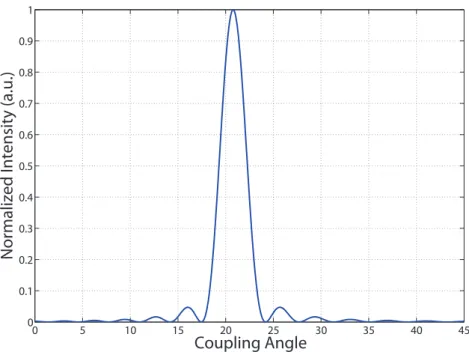
CHAPTER 2. THEORETICAL BACKGROUND 13 0 5 10 15 20 25 30 35 40 45 0 0.1 0.2 0.3 0.4 0.5 0.6 0.7 0.8 0.9 1 Coupling Angle N o rm alized Intensity (a .u. )
Figure 2.2: Total intensity as a function of coupling angle in accordance to Eq.2.10 In their work, Ogawa et al. [42] derived a solution of Eq.2.9 with an approach borrowed from microwave optics called transmission line formalism. This ap-proach considers a travelling wave through a tranmission line and works out the voltage drop during transmisison. Transmission line formalism approach leads to eigenmodes as follows:
ψ(β, z) = sin [(β− β0)iΛ/2]
π(β− β0)iΛ exp[j(β− β0)iΛ/2]· exp[−jβz], which leads to total power with ψ∗ψ, taking i = 1,
I ∝ sin
2[(β− β0)Λ/2]
[π(β− β0)Λ]2 , (2.10)
where β ≃ β0and β = k0sin θ. This equation is useful for calculating the coupling
2.2
Taper Structure and Waveguide
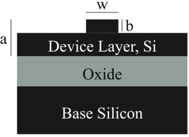
The light coupled into the chip need to be guided through the cantilever to the photodiode. Conveying the light through the cantilever is the most important part of the sensor in this work, since the act of this guidance is the mechanism that produces the optical signal as the cantilever oscillates. As the cantilever oscillates, there occurs a change in optical path length, and this causes the change in the intensity of the light that is guided to the photo diode.
Base Silicon
Device Layer, Si
Oxide
a
b
w
Figure 2.3: Physical parameters for the waveguides in this work.
In integrated optics, waveguides are features that can guide a beam of light through itself. One can achieve such a behavior by making refractive index of the waveguide slightly bigger than its surroundings. Bigger the difference between refractive indices of guide and its surrounding media, the better confined the wave becomes. The most basic wave guide is a slab waveguide. It lies between two layers, and the light is confined in one dimension.
A taper structure is a special kind of waveguide which has different dimensions on both end (Fig. 2.4). A gradual slow change in dimensions ensures an adiabatic route for coupling. Taper structures are employed to couple a light from a wider source to a narrower one[43]. In this work we have used the taper structure to couple the coupled light from the grating coupler to the waveguide. Width of the initial port was on the order of 100 µm’s and the width of the waveguide differed between 50 µm’s to 5µm’s.
CHAPTER 2. THEORETICAL BACKGROUND 15
Figure 2.4: A taper is a waveguide with different dimensions at each end. So
w1 ̸= w2 and h1 ̸= h2.
In this work, a ridge waveguide is employed. In this case, confinement in the second dimension is done by machining a rib where the wave is guided, see Fig.2.3.
Grating
Cantilever
Taper Structure
Waveguide
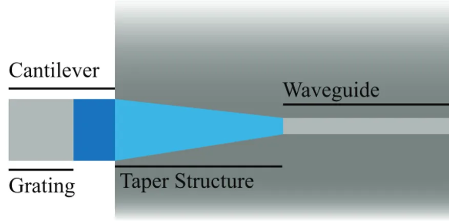
Figure 2.5: Top view of the sensor. There are four components: grating coupler, cantilever, taper structure, and waveguide.
There are several methods to investigate the supported modes of a waveguide. The easiest method is effective index method. This method works out the index that travelling wave sees and gives the supported modes. Formalism strongly resembles basic quantum well calculations in a standard quantum physics text, this method has been givin in [44] and will not be repeated here. While effective index method is easy to implement in channel waveguides, taper structure is difficult to model with this method. We have modelled these structures with a more detailed mothod.
Taking the Helmholtz equation (Eq.2.7),
∇2
Ψ + k02n2(x)Ψ = 0. (2.11)
If the refractive index has a isotropic behavior, wave function can be decomposed into plane waves,
Ψi(x, z, t) = Ai(x, z)ej(kxx+kzz)ejωt+ c.c. (2.12)
Here a further simplification can be made if the wavefront and the index change is slow. If Ai, are assumed to vary slowly, then,
∂2Ai(x, z)
∂z2 = 0. (2.13)
With this last approximation, Helmholtz Equation becomes [45] [ ∂2 ∂x2 + k 2 0(n 2 x− n 2 z) ] A(x, z) =±2jk0nz ∂Ai(x, z) ∂z . (2.14)
This assumption is called the paraxial assumption and this equation is the parax-ial wave equation. This equation can be solved with several methods. A Fourier transfor can be made and resulting waves can be solved and then a back trans-form ban be made. However, an easy and a reliable way is to use finite difference method to solve this paraxial equation. In this method, a computation window is selected and broken into a grid structure (Fig. 2.6). The domians in the grid structure should be large enough to reduce the computational complexity and also small enough to properly model the index distribution.
Now we can convert Eq. 2.14 to its finite difference counterpart. This is done by employing Taylor expansion to each adjacent point in each dimension,
ψ(x + ∆x) = ψ(x) + ∆x∂ψ(x) ∂x + (∆x2) 2 ∂2ψ(x) ∂x2 +· · · and ψ(x− ∆x) = ψ(x) − ∆x∂ψ(x) ∂x + (∆x2) 2 ∂2ψ(x) ∂x2 − · · ·
adding these together we can obtain finite difference expression for the second derivative,
∂2ψ(x) ∂x2 =
ψ(x + ∆x)− 2ψ(x) + ψ(x − ∆x)
CHAPTER 2. THEORETICAL BACKGROUND 17
Figure 2.6: In finite difference technique, a computation window is selected and broken into a grid structure.
Choosing planar waves as a wave function, one can solve the paraxial equa-tion by using this finite difference method. In fact, this whole approach is called beam propagation method.[46] It solves the paraxial wave equtaion by decom-posing the wave into planar waves, each travelling to a direction slightly different than the others. Decomposition and recomposition is done via discerete Fourier transform. BPM makes two assumptions, first of which is the fact that a travel-ling wave diffracts as it propagates through space, and the second assumption is that the accumulated phase shift due to propagation depends on the local index of refraction [45]. For this work, BeamPROP from RSoft Inc. is employed [47].
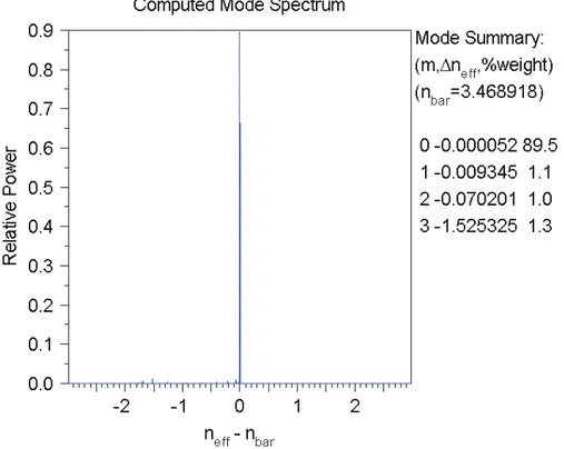
BPM method is employed for calculations of the mode spectrum, i.e., how many modes that this taper and waveguide structure supports and what happens to the travelling wave. For simulations, waveguide with width w = 5 µm and rib height (i.e. a− b) of 1 µm is selected (See Fig.2.3). 1µm rib height is very high. However, it is a good limit to check if the waveguide is still within the boundaries of expected operation consitions if it is over etched.
Mode spectrum can be investigated in Fig.2.7. Mean refractive index, nbar is
which means wave travels through the silicon waveguide layer as intended. Also there are four modes supported by this structure, however, as one can see, modes other than the fundemental one have very small relative powers (1.1% for the first excited mode, 1.0% for the second excited mode, and 1.3% for the third excited mode) and their effective indices are more far apart than the fundemental mode. Since silicon crystal has a high refractive index contrast, obtaining a single mode waveguide is quite difficult. It requires a small rib height and a large width, which makes the whole fabrication cumbersome. Instead, we made the waveguide langth as long as possible to let the other modes leak, so that only the fundemental mode reaches to the end. This kind of single mode waveguides are called quasi-single mode waveguides.
Fundemental mode is the one that has the most parallel propagation vector to the propagation direction, so it is less prone to decoupling to other modes as it propagates.
Figure 2.7: Computed mode spectrum using BeamPROP software.
CHAPTER 2. THEORETICAL BACKGROUND 19
The profile is taken at a crossection of the taper structure.
0.0 1.0 Computed T ransverse Mode Pro (m=0,neff=3.46882)
Ho zontal D ec on ( m) 30 - -20 -10 0 10 20 30 V er t al D ec o n ( m ) 0 1 2 3
Figure 2.8: Field profile of the fundemental mode at a cross section of the taper structure.
Even though, its fundemental mode is the most suitable mode for this sensor, it is not crucial for operation. Since optical path difference affects all modes, any travelling mode can be employed for measuring the total power variation. Nevertheless, fundemental mode should be used for the measurements, since the fundemental mode has the most parallel component of the propagation vector. If some other mode is employed, due to the dynamic nature of the sensor, this mode can couple in higher modes.
2.3
Cantilever
Arguably, the most important part of the sensor in this work is the cantilever beam, since the sensing is mainly done by deflection of this beam. A cantilever beam with high resonance frequency is a good choice to prevent noise. However,
if the beam is too stiff then contact mode operation will cause sample damage. In this work, we have considered commercial size cantilevers with resonance fre-quencies ranging between 10 KHz to 100 KHz. For a typical cantilever in this work (with dimensions 450 µm of length, 120 µm of width, and 3 µm), assuming silicon crystal has density of 2.3 g/cm3, with resonance frequency of 26 Khz, the cantilever will have spring constant of 0.25 N/m, which is way smaller than 10 N/m.
Fundemental natural frequency of a camtilever beam can be calculated by starting from the natural frequency of a spring [48]
ωo = 1 2π (√ 5 3 √ E ρ ) h L2, (2.16)
where E is the Young’s modulus of the material, L is the cantilever length, h is the centilever thickness, ρ is the mass density of the material. For silicon the ratio √
E/ρ is 8200 m/s [49]. One thing to notice is that width of the cantilever does
not affect the natural frequency. By using this rough model, we can calculate the natural frequency of our cantilever as 14 KHz. However, for more accurate solutions a more detailed analysis has to be done.
Deformation can be broken into three major parts, namely elastic deformation, thermal deformation, and the deformation already on the material, i.e., initial deformation. If elastic deformation is formulated as,
⃗δ = u(x, y, z)⃗i + v(x, y, z)⃗j + w(x, y, z)⃗k,
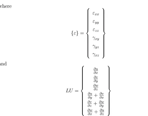
then a general state of the strain can be described with six independent compo-nents, εxx = ∂u ∂x εyy = ∂v ∂y εzz = ∂w ∂z γxy = ∂u ∂y + ∂v ∂x γyz = ∂v ∂z + ∂w ∂y γxz = ∂u ∂z + ∂w ∂x or in matrix form {ε} = LU (2.17)
CHAPTER 2. THEORETICAL BACKGROUND 21 where {ε} = εxx εyy εzz γxy γyz γxz and LU = ∂u ∂x ∂v ∂y ∂w ∂z ∂u ∂y + ∂v ∂x ∂v ∂z + ∂w ∂y ∂w ∂x + ∂u ∂z
from this expression a stress matrix can be formed by using generalized Hooke’s
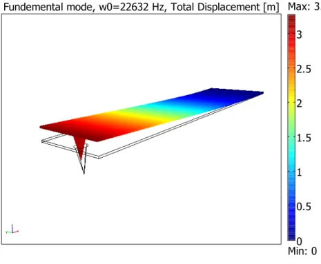
Figure 2.9: Fundemental vibration mode of a cantilever beam with 450 µm of length and 125µm of width and 3 µm thickness.
Law. Elements of stress matrix can be derived via following relations,
εxx = E1 [σxx− ν (σyy + σzz)]
εyy = E1 [σyy− ν (σxx+ σzz)]
εzz = E1 [σzz− ν (σxx+ σyy)]
γxy = G1τxy γyz = G1τyz γzx= G1τzx,
where E is the Young modulus and G is shear modulus. These can be represented in a matrix form as follows
{σ} = [ν]{ε}. (2.18)
Stress and strain matrices can be used to define strain energy integral, Λ(e) = 1
2 ∫
V
[σ]T{ε}dV. Substituting Eq.2.18 into this equation gives
Λ(e) = 1 2
∫
V
{ε}T[ν]{ε}dV. (2.19)
Minimization of this energy can be done with finite element analysis (FEA) [50]. Finite element analysis is a computational method to work out approximate so-lutions to boundary value problems. Its methodology resembles finite difference methods, however, instread of a steady grid, FEA employs a mesh. Mesh con-struction is an integral part of FEA, it depends on the physical structure of the specimen and takes its shape accordingly, hence covers most of the important points in calculation. In contrast, finite difference method a grid is formed re-gardless of the physical structure of the specimen. Grid covers the space through which the integral is evaluated. [51]
In this work, a software implementation of FEA, COMSOL [52] package is employed for stress-strain calculations. For a silicon crystal cantilever with 450
µm of length and 125 µm of width and 3 µm thickness, fundemental vibration
frequency is found to be 20761 Hz (See Fig.2.9). Also heigher eigenmodes of vi-bration was calculated as 1298587 Hz, 152551 Hz, and 3645444 Hz (See Fig.2.10). Additionally, to further foresee the effect of an attached tip on the natural frequency, we have modelled a cantilever with a conical silicon tip attached. A
CHAPTER 2. THEORETICAL BACKGROUND 23
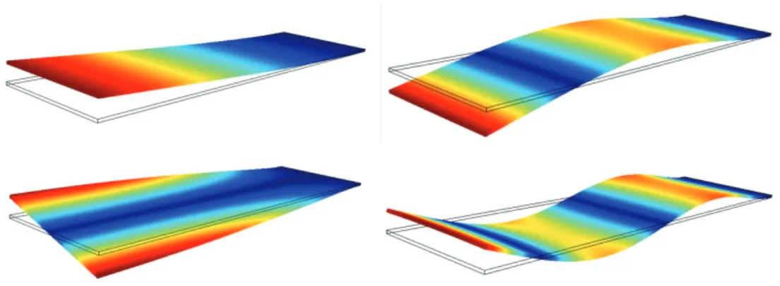
Figure 2.10: First four modes of a cantilever beam with 450 µm. of length and 125 µm of width and 3 µm thickness. From top left to bottom right, fundemental, first, second, and third excited vibration modes having 20761, 1298587, 152551, 3645444 Hz resonance frequencies respectively.
tip with 40 microns of height and 10 microns of radius is attached numerically at 20 microns apart from the deflecting side of the beam. Based on our calculations, natural frequency increased by the order of nearly 2 KHz (See Fig.2.11).
Figure 2.11: Addition of extra load of tip increases the natural frequency of the cantilever nearly 2 KHz.
Chapter 3
Experiment
In this chapter, production of grating loaded cantilever sensor will be discussed in detail, and experimental setups will be explained.
3.1
Introduction
There are three main logical steps in production of a grating loaded cantilever. First grating couplers are produced. Then, taper and waveguide structures are defined and finally cantilever itself is realized. There are half a dozen of sub steps and tens of small steps in production. These make the production yield very low since even if 90% yield is obtined from each step, total yield will be 53% in 6 steps [53].The whole production is done in Class 100 clean room environment and with standard cleanroom equipment.
Production of the sensor is done with a silicon on insulator (SOI) wafer. These are basically two silicon wafers, thermally oxidized and then transfused like a sandwich. A cross-section of a sample SOI with a transferred grating can be seen on Fig.3.1
After fabrication, a computer controlled measurement setup is used to make all measurements. We have developed the needed computer interface in LabVIEW.
Figure 3.1: Cross-section of a Silicon on Insulator wafer.
A motorized stage, powermeter, lock-in amplifier, piezo element is contolled with this software. Computer control ensured consistency between measurements and rectified human error element.
3.2
Fabrication
3.2.1
Mask design
For the fabrications, a photolithograpy mask was designed in L-Edit software. This software is an industry standard for computer aided photomask design. As it can be investigated in Fig. 3.2, the mask we have designed has three main parts, grating area, taper structure and the waveguide, and finally the cantilever. We have also designed a second mask to try KOH etching, which had one more cantilever definition step.
A photomask, is basically a chromium patterned quartz or soda lime glass of 10 cm× 10 cm dimensions. Patterned chromium gets in contact with the photoresist
CHAPTER 3. EXPERIMENT 27
and prevents the shone UV light from reaching the resist. A photomask can be used several hundred times. Generally a nanometer resolution is needed for integrated optical applications.
There are some design principles during mask design. First of all, a calibration waveguide without a cantliever must be put into the design to calibrate the mea-surement setup. This waveguide should have at least 50 µm width to effortlessly detect the coupled light. Also, in order to make measurements easier, all grating couplers must be aligned on a straight horizontal line, so that after calibration, only a change in the lateral direction would change the cantilever under test.
Figure 3.2: A schematic explanation of the mast we have designed. It has three main steps. Grating coupler area, waveguide and the taper structure, and the cantilever.
3.2.2
Grating Transfer
Grating production, in itself, is a cumbersome task. There are several ways to produce gratings. FIB etching, interference lithography, etc. [54] In this work, a high quality monochromator grating with 1800 grooves per millimeter and 550 nm period is transfered onto the SOI chip. Transfer is done with nanoimprint lithography.
At the very beginning, a 1.5×1.5 inches glass sample of monochromator grat-ing is cut and used as a master for a PDMS polimer mold. PDMS polimer mold takes the shape of the surface of the grating master (Fig. 3.3.a). After polimer-ization, PDMS negative can be used several times. If PDMS negative distorts in any way, a new PDMS master can easily be produced.
Canvas chip is a SOI wafer with 1.5×1.5 centimeter square, cleaved from a SOI wafer with device thickness ranging from 1.5 µm to 5 µms. Device layer thickness is crucial, since thicker this layer, higher the cantilever’s resonant frequency, and stiffer the cantilever itself becomes.
After standart cleaning procedures, a UV curible polimer, OG 146 from Epoxy Technology Inc. is spin coated onto the surface. PDMS negative is adhered to the polimer coated surface minding the alignment of crystal planes and grating grooves(Fig. 3.3.b,c). Since before measurements, waveguides should be cleaved to get a clean facet, waveguides should be patterned according to the crystal planes. And to couple incident light to the waveguide, this same attention must be paid for grating transfer. Grooves of the grating should be perpendicular to the waveguide.
After adhesion, chip bearing PDMS negative is baked in a UV oven for more than 7 mins. This step cures the OG 146 polimer and concludes the polimerization step. After curing, PDMS negative is peeled off and a polimer grating is coated onto the silicon surface. After this step, a reactive ion etching process can easily transfer the grating onto the chip, however, desired design is to load only the tips of the cantilever with gratings. Thus this tip area should be defined.
Grating area definition is done by standard photolithography. A photo resist polimer, AZ 5214 from AZ Chemicals is spin coated onto the surface of the chip. Grating area mask is got in contact with the resist and a UV light with 350 nm wavelength and 4 watts power is shone onto the chip (Fig. 3.3.d). Photomask covers the areas where gratings will be. Thus another bake and flood expose is applied to reverse the image. After development, resulting pattern is only the grating areas are open, and rest is coated with photoresist.
CHAPTER 3. EXPERIMENT 29
a)
b)
c)
d)
e)
f)
g)
h)
i)
j)
k)
l)
Now the resist will be the mask in reactive ion etching process. Silicon crystal is etched in a fluorine rich environment [55]. So reactive ion etching is done in an environment of 26 µbar pressure with gases SF6 and O2 with 27 : 7 sccm
flow rates by applying a 200 W plasma (Fig. 3.3.e). In aprroximately 3 mins (which can vary from laboratory to laboratory), desired areas are patterned with gratings.
Figure 3.4: Cross-section of a Silicon on Insulator wafer, with transferred grating on device layer.
Finally a piranha solution can be employed to rinse unwanted polimers from the surface. Piranha solution is prepared by adding 1 part H2O2, peroxide, to 3
parts H2SO4. Usually, acids are added to water, however in this case a water based
substance is added to the acid. Piranha solution can etch all organic materials and makes the surface hydrofilic, which eases the adhesion of polymers. Piranha rinse has similar effects like oxygen plasma.
CHAPTER 3. EXPERIMENT 31
3.3
Taper Structure and Waveguide Pattern
Taper structure, which eases optical signal to the waveguide guiding the signal to photo detector, and the waveguide itself is patterned in one session via standard photolithography process.
Grating loaded chip, rinse cleaned with piranha solution, is sputtered with chromium via physical vapor deposition (Fig. 3.3.f). Sputtering is done with accelerating argon gas onto a chromium target and ionizing chromium atoms, which are then sputtered onto the surface of the sample. This sacrificial chromium layer will be patterned with taper structure and waveguide, then will be used in reactive ion etching.
Patterning onto the chromium surface need one more extra step. An adhesion promoter, HMDS, is spincoater before AZ 5214 photo resist to further enhance adhesion (Fig. 3.3.g). After develop process, a 3min post bake to solidify the resist is done before immersing the sample into chromium etchant. At the stage of chromium etching, photoresist is the mask. In this step an extra care not to tilt the solution should be paid to avoid undercuts by etch solution. A DI water rinse is done after chromium etch process.
For the last step, sample, having a chromium layer patterned with taper structure and waveguide, goes through rective ion etching process again for 3mins (Fig. 3.3.h). After RIE excess polimers are rinsed off with piranha solution and chromium mask is etched with chromium etchant. A DI rinse makes the sample ready for the next step (Fig. 3.3.i).
3.3.1
Cantilever
Cantilever production is the most crucial step in the whole production, since the whole purpose of this work is to produce a cantilever sensor. However, before this step, testing the grating and waveguides would help avoid to continue with a faulty sample.
At this stage sample is sputtered with chromium again. This time to give the definition of cantilever beam. Standard photolithography procedure is applied to pattern the chromium mask and RIE is employed to etch away the unwanted device silicon and further etching is done to get rid of oxide layer at the same areas(Fig. 3.3.j).
Now the employment of SOI wafer shows itself, when the sample is left for several hours in an Hydrofloric (HF) acid solution to remove the oxide under the cantilevers to get a nice undercut (Fig. 3.3.k). In order to stop etching alcohol is used to replace the HF solution. Oxide layer is approximately 3µm thick, which makes blow dry the sample difficult, due to capillary effect, as liquid is removed from the undercut region can make suspended cantilever beam snap onto the base silicon. At this point a more careful approach is employed. We used a critical point drier, which replaces liquid alcohol with liquid carbondioxide and releases the pressure so that the critical point at which cabondioxide is in phase transition from liquid to gaseous form. This way, a more careful drying is achieved and a possible snapping is prevented (Fig. 3.3.l). A completed sample can be seen in Fig. 3.5
Figure 3.5: SEM micrograph of the sample cantilever. Inset shows the grating structure.
We have devised another way to release the cantilever: KOH etch. This method exploits the fact that KOH solution etchs silicon crystal in an anisotropic
CHAPTER 3. EXPERIMENT 33
fashion. That is, it etches (100) crystal plane faster than (111). As a result a deep undercut can be obtained. However, since the device itself is made up of silicon crystal, a way to protect the device should be devised.
KOH solution etches silicon oxide very slowly and does not etch silicon nitride at all. If one can envelope the device between the oxide layer of the SOI chip and a film of silicon nitride, the ramifications can be rectified. Result of tour first attempt to release the cantilever with KOH etch can be observed in the optical microscope images in Fig. 3.6.
Figure 3.6: Our first attempt to release the cantilever with KOH solution. For a good film coverage at the edges of device, cantilever definition should be given with a special chemical solution of nitric acid, hydroflouric acid, instead of rective ion etching. This solution also gives an anisotoropic etch profile, however it does not etch chromium, thus, a chromium mask can be used to give the cantilever definition.
A slanted edge profile increases the film thickness at the edges. A PECVD film growth of silicon nitride and a new cantilever definition with wider coverage will envelop the device. At the bottom, the oxide of the SOI, and at all other parts, nitride film can protect the device during KOH etch.
Although difficulties of the critical point dryer has been overcome, this method has proven to be a lot difficult to implement. We are currently working on the calibration of this process.
3.4
Measurements
Measurements are done on a single setup. A solid state laser having a peak wavelength of 1550 nm with spectral bandwidth of 0.2 nm is used as the source. This wavelength is ideal for measurements since sensor is made up of silicon crystal, which is transparent to this wavelength.
Camera or Intensity Detector a b Lens Sample Piezo Element Incident IR Beam Incident Angle Lock-in Amplifier Sine Out Pre-Amplifier Input
Figure 3.7: Measurement setup.
There are two stages of measurement. First, coupling angle of the grating coupler is measured for future reference and to check whether the coupler, taper structure, and the waveguide works properly. At the second stage remaining measuremetns are done in one session.
CHAPTER 3. EXPERIMENT 35
Element Function Notes
Laser diode Light source Peak wavelength at 1550nm
Rotary stage Control incident angle Step size 0.01 degrees
Piezo element Excite the sample at given frequency
Lens Collect output signal from
waveguide
Detector/Camera Convert light signal to electrical one
Preamplifier Amplify the electrical signal A low noise amplifier is employed
Lock-in amplifier Phase sensitive detection Also used as a function generator to drive pizeo element
Table 3.1: Elements in the measurement setup and their functions. A detailed list of measurement inventory can be found in Table 3.1 and their usage can be investigated in Fig. 3.7.
The incident angle is changed by a motorized stage which is controlled by a computer program that we have developed in LabVIEW. Also the photo diode readout is sampled by our program. Our program can distinguish meaningful power readings from the errors, which is not done by the readout circuit itself. Also we could take as many measurements as we could for one incident angle, which reduced the random noise significantly. Since the whole measurement setup is computer controlled, we could repeat the measurements several times with high precision and get rid of the human error.
3.4.1
Coupling Angle
Coupling angle measurement is done to ensure production quality so far and for future reference. A motorized rotary stage, controlled by a computer program is employed for controlling the incident angle. For each 0.01 degrees of rotation,
photo detector is queried for power amplitude for several times to get rid of ran-dom error in measurement. All measurements are done in sun proof environment to avoid background noise as much as possible. In Fig. 3.8 one can observe the coupled light at this stage.
Figure 3.8: Coupled light as it is seen from the end of the waveguide.
3.4.2
Resonance and Sensitivity
At this stage, finished sample is attached to a pizeo element with resin, and vibrated with a function generated by lock-in amplifier. Incident angle of the light source is fixed at the half point between the coupling angle of the grating coupler, and the deepest point in its descent. This way, every change in the power amplitude is magnified by the quality factor of the peak, since the differential at this point is the highest.
Coupled light signal is collected with photo diode and converted into an electri-cal signal. Then this signal, having the same frequency as the vibration frequency of the pizeo element, is analyzed by the lock in amplifier. A resonant curve is expected to be observed at the natural frequency of the cantilever. Also a waveg-uide without a cantilever was employed to check whether the signal is generated by the cantilever vibration or the resonance of the piezo element.
CHAPTER 3. EXPERIMENT 37
Sensitivity measurement is a way to backtrace the whole experiment. Keeping the driving frequency fixed, incident angle of the source is changed, which gave the derivative of the coupling angle curve.
Results
4.1
Coupling Angle
As it was explained in Sec. 3.4, coupling angle measurement shows the incident angle at which incident light is maximaly coupled into the chip through grating coupler. As it can be seen in Fig. 4.1, maximum coupling occurs at 34.9◦. The second peak occurs due to a second travelling mode through the waveguide. This is expected since the design of the chip has several kinds of waveguide structures, widths ranging from 5µm to 50µm. This measurement is done with a waveguide of 20µm waveguide, which is a multimode waveguide. Two modes appear in two different angles because two modes have two different momenta.
Difference in coupling angle is a good indicator of the momentum difference between two modes, thus effective index that these two modes feels. One can calculate effective indices of these two modes by employing the match condition (Eq.2.2). A little modification yields,
k0sin θ = k0neff− 2π Λ which yields neff = ( sin θ + λ Λ ) , 38
CHAPTER 4. RESULTS 39 32 33 34 35 36 37 0,0 100,0n 200,0n 300,0n 400,0n 500,0n 600,0n 700,0n 800,0n 900,0n 1,0µ 1,1µ 1,2µ 32 33 34 35 36 37 I n t e n si t y ( W a t t ) Angle (°) Intensity
Figure 4.1: Coupling angle results. Double peak means coupled light is not a single mode signal. In this case two modes are travelling.
where λ is wavelength of the incident light, Λ is the period of the grating. So the fundemental mode having coupling angle of 34.9◦ has the effective index of
nfundemental = 3.39, and first excited mode, having a coupling angle of 34.2◦ has
effective index of nfirst = 3.38.
Nevertheless, fundemental mode has the greatest power. The peak has quality factor of 102.6, which could be better. However it is enough to get displacement measurements.
Also taking the difference of the matching condition would yield, cos θ∆θ = ∆k
k0 ,
which gives an understanding of how many wavenumbers were needed to resolve these two modes,
∆k = k0cos θ∆θ.
Fundemental peak is at 34.9◦ with FWHM of 0.339◦. These correspond to ∆k = 197cm−1.
Coupling angle measurement also reveals the range that the frequency re-sponse is the highest. This calculation can be done by employing a well known signal processing concept, available dynamic range, which is used to character-ize an amplifier [56]. We look for the range that the measurement bandwidth becomes the natural noise bandwidth [56]. In our case signal drops to its half from angle 34.87◦ to 35.9◦, which corresponds to 3.84 mrad. This translates into a dynamic range of 13 mrad% .
4.2
Resonance and Sensitivity
Resonance curve measurement gives the netural frequency of the cantilever. Also a spectral analysis at this stage gives noise structure. There are several issues that need to be addressed to confirm the validity of the measurements. One of which is the spectral response of the piezo element (See Fig. 3.7). In order to test whether the signal is generated by the resonance of the cantilever, or the resonance of the piezo element, calibration waveguides are employed. These waveguides have 100µm’s of width,so they can be easily seen during experiment setup. Also they have the same grating coupler at their tip. However, they do not have cantilever structures, so if photodiode is positioned at the end of these waveguide, if a resonant signal is read, it would be from the piezo element itself. This test of validity was successful.
The second caviat is the existance of multiple peaks. There are 36 cantilevers on one chip (See Fig. 4.3), which may make vibrational modes of other cantilevers to couple into every other one. In order to test all the vibrational modes, instead of coupled light, reflected light was measured against frequency, see Fig. 4.2. The strongest peak is the peak of the cantilever. We beleive that the second peak occurs due to its neighboring undercuts, however, this needs to be testedfurther. Also, there are several peaks belonging to other released waveguides.
After these tests, a proper resonance measurement can be done. Coupling the photodiode at the end of the waveguide, intensity of the light coupled from the
CHAPTER 4. RESULTS 41 20,0k 25,0k 30,0k 35,0k 40,0k 45,0k 50,0k 0,0000 0,0001 0,0002 0,0003 0,0004 0,0005 0,0006 I n t e n si t y ( a . u . ) Frequency (Hz)
Figure 4.2: All vibrational modes measured from the reflection off the cantilever. grating coupler is measured. A resonance peak at the natural frequency of the cantilever is expected. Resonance measurement can be investigated in Fig. 4.4.
Cantilever resonates at 26.5KHz. Resonance peak has 27.2 quality factor. This is relatively low, however one should bear in mind that all measurments are done in atmosphere without a good vibration isolation. Further vibration isolation and a vacuum environment would increase this quality factor. Resonance frequency is nearly 6 KHz off compared to the findings in Sec. 2.3. This is due to the overly undercut portion of the cantilever, which further elongated the cantilever. Also neighboring undecuts were not modelled in Sec. 2.3.
Also to confirm the resonance phenomena, phase of the incoming signal was measured against changing frequency, at resonance peaks, phase changes direction (See Fig. 4.5). This phase change is due to the working principle of the lock-in amplifier, or phase sensitive detector (PSD). The PSD multiplies the reference signal with the speciment signal and looks for the phase difference. If the phase difference dissappears, the signal is locked to the reference. So, after each lock, the derivative of the phase should change direction.
Figure 4.3: There are several cantilevers on the chip (36 to be exact), which causes resonant frequencies of neighboring cantilevers to appear on every measurement.
26567 Hz
Figure 4.4: Resonance curve of the cantilever, taken with increasing vibration amplitude. Unwanted peaks occur due to coupling of neighboring undercuts.
CHAPTER 4. RESULTS 43 25000 26000 27000 28000 29000 -6 -5 -4 -3 -2 -1 0 25000 26000 27000 28000 29000 S i g n a l P h a se ( R a d i a n s) Frequency (Hz) Signal Phase
Figure 4.5: Phase as a function of frequency. A good way to check resonance condition.
In order to backtrack the consistency of the measurements, frequency was fixed at the resonance peak and incident angle was changed. Expected result is peak formation at the angles with the highest sensitivity. In Fig. 4.7 one can see that indeed a derivative of the coupling angle curve is obtained, where turning points in coupling angle curve yield zero in this curve and slopes correspond to peaks. The heighest sensitivity points can easily be seen from this curve. Also the direct derivative of the coupling angle curve can be investigated in Fig. 4.6.
33,8 34,0 34,2 34,4 34,6 34,8 35,0 35,2 S e n si t i vi t y ( a . u . ) Incident Angle (°)
Figure 4.6: Direct derivative of Fig. 4.1.
33 34 35 36 37 0,0000 0,0002 0,0004 0,0006 0,0008 0,0010 0,0012 0,0014 33 34 35 36 37 P o w e r D e t e ct o r R e a d i n g A m p . e d ( A ) Angle (°)
Power Detector Reading Amp.ed
Figure 4.7: Sensitivity as a function of incident angle. This measurement back-traces the whole experiment. This curve shows incident angles with best sensi-tivity.
Chapter 5
Conclusion and Suggestions
We have proposed a new sensor to detet the deflections of a scanning probe microscopy cantilever. As the cantilever bends, optical path changes since a good proportion of the optical path lies on the cantilever. A grating coupler is loaded on top of the cantilever to couple an incident light into the optical circuit. Optical circuit started with a taper structure, designed to convey the optival signal to a narrower waveguide adiabatically.
We have designed a photolithography mask and a fabrication pipeline. We have fabricated the proposed sensor with standard microfabrication procedures in a Class 100 cleanroom environment with standard cleanroom equipment. Then we have tested the sensor in a measurement setup of our own design. A computer program was developed to control the measurements at each step.
A resonance frequency of 26.5 KHz was observed with a quality factor of 27.2. This result is verified by testing the same setup without a cantilever. The piezo element did not have a resonance peak in the vicinity of this frequency. Also a sensitivity measurement verified the coupling angle measurements.
In light of our observations, the integrated optical approach proposed in this work is a good candidate for deflection sensing. It has many adventages over the sensing techniques in use today. The most importan of which is, being an
embeded design, minimal effort is needed to calibrate the measurement setup. Also with employment of GaAs substrate, a light source and a detector can also be embeded onto the chip which would make UHV applications dead easy. And no calibration would be needed in such a scenario.
Eventhough all measurements are done in atmosphere, a reasonable qual-ity factor for displacement measurements is obtained. Further enhancement in vibration isolation would increase ther signal to noise ratio. Also a vacuum envi-ronment, or at least a steady air would increase the quality factor.
Fabrication pipeline in this work has over a dozen main steps, which begs the utmost attention at each step to ensure high yields of production. However, since only standard techniques are used at each step, the whole pipiline can easily be fitted into industrial production.
To conclude, our proposed design has many premises and is a viable alternative for displacement measurements.
![Figure 2.1: Physical parameters for a typical grating surface. [1]](https://thumb-eu.123doks.com/thumbv2/9libnet/5770048.116975/21.892.328.638.233.361/figure-physical-parameters-typical-grating-surface.webp)