Wireless Corner
Christos Christodoulou
Department of Electrical and Computer Engineering
Eva Rajo-Iglesias
Departamento de Teoria de la Sel'lal y Comunicaciones University Carlos III of Madrid, Despacho 4.3810
University of New Mexico
Albuquerque, NM 87131-1356 USA Tel: +1 (505) 277 6580
Avenida de la Universidad, 30,28911 Leganes, Madrid, Spain Tel: +34 916248774
Fax: +1 (505) 277 1439 Fax: +34 91 6248749
E-mail: [email protected] E-mail: [email protected]
On the Capacity of Printed Planar
Rectangular Patch Antenna Arrays in the
MIMO Channel:
Analysis and Measurements
Celal Alp Tunc1, Ugur Olgun2, Vakur B.
Ertiir,c,
and Ayhan Altintas3
1Ankara Research and Technology Laboratory (ARTLab Ltd) Ankara, Turkey
2The Ohio State University, ElectroScience Laboratory Columbus, OH 43212 USA
3Department of Electrical and Electronics Engineering Bilkent University
Bilkent, Ankara, TR-06800, Turkey E-mail: [email protected]
Abstract
Printed arrays of rectangular patch antennas are analyzed in terms of their MIMO performance using a full-wave channel model. These antennas are designed and manufactured in various array configurations, and their MIMO performance is measured in an indoor environment. Good agreement is achieved between the measurements and simulations performed using the full-wave channel model. Effects on the MIMO capacity of the mutual coupling and the electrical properties of the printed patches, such as the relative permittivity and thickness of the dielectric material, are explored.
Keywords: MIMO systems; antenna arrays; microstrip antennas; microstrip arrays; planar printed arrays; antenna array mutual coupling; moment methods
1.
Introduction
M
icrostrip patch antennas have gained immense popularity in
military and commercial applications, owing to their con
formal, lightweight, and low cost nature. Moreover, the recent
decline of low-loss dielectric substrate prices has boosted their
utilization, particularly in commercial communications applica
tions. Their performance in multiple-input multiple-output
(MIMO) systems thus seems very promising [ 1-8], but has to be
investigated in detail.
In [
9], the M IMO performance of printed dipole arrays was
analyzed using a full-wave channel model, based on the Method of
Moments (MoM) solution of the electric-field integral equation
(EF IE). Comparisons with freestanding dipoles were given in
terms of the channel capacity. Effects of the electrical properties of
printed dipoles on the M IM O capacity were explored in terms of
the relative permittivity and thickness of the dielectric material.
In this work, the study on printed dipoles
[9]is expanded by
modifYing the full-wave channel model developed before for ana
lyzing probe-fed rectangular patches. Several probe-fed rectangu
lar microstrip patches are fabricated and employed in a M IM O
wireless communication system. The performance of different
patch antenna arrays in terms of MIMO channel capacity is meas
ured and the results are compared with each other, as well as the
numerical results of the full-wave channel model.
2.
Wireless Channel Measurement Using a
Vector Network Analyzer
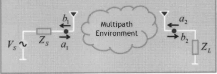
Let us consider the wireless communication system with sin
gle antennas at the transmitter
(T
X) and receiver
(RX)sides as
illustrated in Figure
I.Using network analysis, the total port volt
ages and currents at the terminal planes for the transmitter port
(port
I)and the receiver port (port 2) can be written as
I
n
=on -bn
� ',,; Zin,n
(I)
(2)
where n
=1,2 .
Zin,n is the input impedance seen through the port,
and is taken equal to the characteristic impedance of the port, ZO,n'
on represents an incident wave at the nth port, and bn represents a
wave reflected from that port. These inward and outward propa
gating waves are related to each other via the scattering (S)
parameters:
( 3)
(4)
The voltage and the current at the transmitting-antenna port then
become
(5) 182 h'".,.L
Multipath +- -a, • Environment-1b2
Zs � Vs '\, al ZLFigure 1. A SISO wireless communication system.
(6)
The source voltage
(Vs) can be expressed in terms of the source
impedance ( Z s ), the port voltage, and the current by
(7)
If the input impedance of the transmitting antenna is matched to
the source impedance, such that
Zin,) = Zs = ZO,) , Equation
(7)turns out to be
(8)
Similarly, when the input impedance of the receiving antenna is
matched to the load impedance
Zin,2 = Z L = ZO,2' the following
relations are valid:
(9)
( 10)
The equality in Equation
(9),taken with Equation ( 10), yields
(II)
and
( 12)
Assuming
Z s = Z L, the channel response defined from the source
voltage to the load voltage can be expressed as
( 13)
which becomes
h=!1l
2 '
( 14)
since
a2 =
O.Namely, if the input impedances of the transmitting and
receiving antennas are matched,
Zin,) = Zin,2 = Zs = ZL '
measur-ing
S2) of such a communication system with the use of a
Table I. The dielectric-substrate parameters.
Antenna A B C
8,
3.0
3.2
4.5
tanb'
0.040 0.045 0.030
d(mm) 1.524 0.508 1.575
Table 2. The parameters of the rectangular patches.
Antenna A B C
W
0.353,1
0.3 39,1
0.301A
L
0.283,1
0.28 1A
0.232,1
FP(x,y)
0.089,1, W/2
0.209,1, W/2
0. 156,1, W/2
port vector network analyzer (VNA) will give twice the channel
response, since the impedances seen through the ports are usually
equal
( Zs = ZL =500). Vector network analyzer systems have
therefore frequently been used to measure the channel characteris
tics of indoor environments [ 10-12]. For the measurement of the
channel-matrix entries of a 2 x2 MIMO system, either a four-port
vector network analyzer alone, or a two-port vector network ana
lyzer with appropriate switches, can be used [ 10].
3.
Design and Production of the
Patch Antenna Arrays
Three sets of low-loss dielectric substrates with copper on
both sides were chosen, the characteristic parameters of which are
given in Table
I.In Table 1,
8,and d represent the dielectric per
mIttIvIty
and
thickness,
respectively.
Furthermore,
tan
0 = a/ (
W808,)
is the loss tangent, which represents the loss
due to the conductivity
( a ).In [1 3], analytical expressions were given for the input
impedance in terms of the characteristic parameters of the rectan
gular patch antenna, such as the width, length, dielectric thickness,
permittivity, and feed-point coordinates, as shown in Figure 2. By
employing these expressions, coax-fed rectangular patch antennas
with 50 0 input impedances were designed to operate at
f
= 1.9725 GHz. The designs were then verified by a commer
cially available electromagnetic solver, based on the mixed-poten
tial integral equation. They were carefully fabricated to make sure
that all antennas were matched to 500 at the operating frequency.
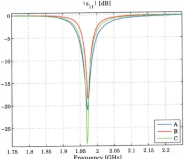
Figure 3 shows curves of the measured
lSI II as a function of fre
quency for the fabricated antennas A, B, and C. The final parame
ters of these antennas (i.e., the width
(W),the length
(L),and the
coordinates of the feed points
[FP(x,y)J)
are tabulated in
Table 2. In Table 2, A represents the free-space wavelength. The
simulated radiation-field patterns of all three antennas are also
illustrated in Figure 4.
Arrays with various configurations were fabricated next. For
each substrate type, mainly two-element arrays were manufac
tured, the antennas of which were located in side-by-side (2 x 1) or
collinear
(lx2) arrangements. To investigate the effects of mutual
coupling on the M IM O channel capacity, antenna elements in an
array were sited either close to (C), or far away (F) from, each
IEEE Antennas and Propagation Magazine, Vol. 52, No. 6, December 20 10
d
w
FP(x,y)
Figure 2. The geometry of a rectangular patch antenna.
0 -5 -10 -15 -20 -25 1.75 1.8 1.85 1.9 '8U' [dB] 1.95 2 2.05 Frequency [GHz] --A --B C 2.1 2.15 2.2
Figure 3. The measured
lSI II
(in dB) as a function of frequency for the fabricated antennas (A, B, C).90 80 60 --A-Ee(9) - - A
-
E.(9) o 180 .... --B-Ee(9)-
-
B -E.(9) C-
Ee(9) C -E.(9) ' " 270Figure 4. The simulated radiation patterns of antennas A, B, and C (the electrical and geometrical parameters of antennas A, B, and C are given in Tables 1 and 2).
Table 3. The fabricated patch array configurations with the distances between the feed points
(l!./
A).
Antenna
Do/A
A l x2C 0.403Alx2F
0.800A2xlC
0.333A2xlF
0.800Blx2C
0.388Blx2F
0.800B2xlC
0.331B2xlF
0.800C
lx2
C 0.351Clx2F
0.800C2xlC
0.282C2xl F
0.800A2x1C
A2x1F
A1x2C
A1x2F
Figure 5. Four different array configurations on substrate A.
other. Table 3 exp
li
ci
tly shows thec
on
figuration
s of thef
abric
ated arrays.In
Table 3, Do denotes the distance betweent
he feed poin
ts ofthe antenna elements in
an array. Note that for the closer element
co
nfigura
ti
ons, the patches were physic
ally
located apart by 0.05,1 . The distance between the feed po
in
ts was therefore differ ent for each substrate, since the patch sizes were different. More over, three single antenn
ason
each substrate were fabricated to be the
transmitting antenna (i.e.,A
J x I,B
Ix
I,C
Ixl)
for the singlei
n
put
si
ngle
-output(SISO),
and single-in
put m
ultip
le-output(SIMO),
cases.Two different configurations were ma
n
ufactured for the receiving array: (i) A I x I for
theSISO case, and (ii)
A Ix2 F
for theSIMO and MIMO cases. B
riefly,17
diffe
rent
patch-antenna/arrayco
nfigurations were fabricated. Four ofthese configurations
are shown in F
igure
5.An
indoor measuremen
tsetup was established at the Antenna
Laborato
ry ofBilkent Un
iv
ersity
.The schematic representation
oft
hesetup is
given inFigure
6. The channel-matrix entries werem
ea
suredwith a
two-portv
ecto
r network analyzer, together with the appropriate switches as expl
ain
edin
[to]. Two 50 n matched184
coaxial swftches,
and two
5 m long pha
se-st
able cables withSMA
c
onn
ect
orsw
ereut
ilized
.The measu
r
ement environment
is
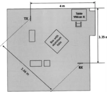
sketched in Figure7.
It was locatedat
the cornerof an
em
pty
room with dimensions 16.5m by
14.5m.
The locations oft
he transmitting and receiving arrays were fixed: the distance between them was 3.66m.
The line ofsight
between
them was blocked
bya
box, which was covered byan
aluminum folio.
The use of alumin
um here wasto
obtain a con ductiveo
bs
tacle,n
am
ely to
inc
rease the reflectio
nsin
the environ ment. There were three other covered boxes in the environment,
al
ong
with ac
hair, a table,and
the vector network
ana
lyzer
plac
edon t
he table, as well.SISO, SIMO, and MIMO m
easuremen
ts were don
e for thearray
confi
gur
ati
on
sgi
ven in
Ta
ble 3. The swi
tches
werecon
trolled by the parallel port of thevector network analyzer,
by applyin
g 3.3 V to one oft
hetransistor-transistor
logic (TTL) in
puts
of the
switc
h, whichn
eeded at l
ea
st 2.5 Vto
alter state. Further more, the transistors required a12
V bias
in
g voltage tooperate,
which was applied by adc
so
urce. One measurement process was formed by 1000 successiverealizations, and corresponding
channel responses (i.e., S21 values) were measured through a 201-point frequency sweep, between
1.75 and2.25
GHz,and saved.
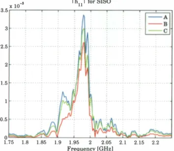
Figure 8 illustrates the average channel coefficients over J 000 differe
n
tmeasurements in
theSISO
case
s for all threeafore-Figure 6. A schematic representation of the indoor MIMO measurement setup. "m
LJD
"""" ".", .' ... /0 ,,;'Figure 7. A sketch ofthe environment.
1.3Sm
3.5 X 10⁻³ , hll' for SISO
[3
-
-B 3 �.-
C 2.5 2 1.5 1 0.5 0 1.75 1.8 1.85 1.9 1.95 2 2.05 2.1 2.15 2.2 Frequency [GHz]Figure 8. The average channel coefficients over 1000 different measurements in the SISO cases for three different transmit ter-array configurations.
(a) SISO 'h 11' for Antenna A
100 50
oL---2.75 2.8 2.85 2.9 2.95 3 3.05 3.1 3.15 3.2 'hu' x 1000
(b) SISO L hll for Antenna A
-96 Figure 9. The histograms of the measured channel response at the operating frequency (1.9725 GHz) for Antenna A: (a) mag nitude, (b) phase.
mentioned antennas. The narrowband channel could be clearly
seen around 1.9725 GHz from the figure. One could expect that the
highest capacity would rise from Antenna A, since the average
channel response was the highest in magnitude.
The histograms of the magnitude and the phase of the chan
nel response at the operating frequency ( 1.9725 GHz) for
Antenna A are given in Figures 9a and 9b, respectively. Note that
because there existed neither moving scatterers nor mobile anten
nas in the environment; in theory, there should have been no varia
tion in the channel capacity. However, very low variations were
observed, most probably due to the inherently unpredictable fluc
tuations in the readings of the vector network analyzer.
Taking the inverse Fourier transform of the channel coeffi
cients, the response could be converted to the time domain. This
IEEE Antennas and Propagation Magazine, Vol. 52, No. 6, December 2010
resulted in a bandlimited version of the channel impulse response,
h
(
t, ,)
, where
tdenotes the time and , is the delay component. As
mentioned, the channel measured here was time-invariant, because
of the absence of moving scatterers or mobile antennas. Hence, the
average power delay profile
(PDP)can be obtained as
I 1000 2
P(,)=- I Hr,,)1 '
1000
r=1
( 15)
where
r
represents one of the 1000 realizations (or time instances).
The normalized average power delay profiles for Antennas A, B,
and C are plotted in Figure 10. Note that the power results greater
than a threshold value are plotted. The threshold was taken as
-25 dB, which is the value the power seemed to contribute before
the line-of-sight path (,= 12.2ns). Investigating the figure, one
could observe that there were two clusters of scatterers, one com
posed of paths with delays between 14 and 45 ns, whereas the
paths in the other cluster had delay components between 45 and
56 ns. Furthermore, the exponential decay of the power (linear on
the dB scale) both within the clusters and between the maxima of
the envelopes could be noticed, which was consistent with [ 14].
The mean excess delay (the mean delay time), which is the
first moment of the given profile, can be expressed as
Ip('k )'k
(,)= kIP(,d
k
The mean square excess delay is given by
Ip('k ),;
(
,2)
=
-,,;;k
I=-p--'(-, k
�
)
k
Power Delay Profile (dB Scale)
( 16)
( 17)
5 r---�---,_---_r---�---�I
�
�I
o -5 -10 - 15 -20 20 30 40 Delay[ns] 50 60Figure 10. The normalized average power delay profiles of measurements for Antennas A, B, and C. The solid black lines represent the exponential decays in the two clusters of scatter ers, whereas the dashed line represents the general exponential decay of the power as a function of delay.
Table 4. The mean excess delay (
(
,)
) and rms delay spread(aT) values obtained from the measurements of three antennas.
Antenna A B C
(
,)
(ns) 31.2 33.0 31
.2aT (ns)
6.9
7
6.5
Finally, the standard deviation of the power delay profile gives the root-mean-square (rms) delay spread:
( 18)
Table
4
shows the mean delay time and rms delay-spread values obtained from the measurements of the three antennas. Note that these delays were measured relative to the first detectable signal arriving at the receiver, which was not necessarily the largest sig nal [ 1 5]. Note also that although all three antennas were placed in the same location and orientation in a fixed environment, the power delay profile, the mean excess delay, and the rms delay spread values were different because of the different transmission characteristics, such as the radiation intensities of the antennas. It could therefore be concluded that the channel was antenna depend ent as well as its response, time-dispersion parameters, and capac ity.5,
Channel Model with Electric Fields
(MEF) for Patch Antenna Arrays
Our channel model with electric fields in [9] used a Galerkin based MoM solution of the electric-field integral equation, in which the currents on the antenna elements (i.e., free-standing or printed dipoles) were modeled with a single piecewise-sinusoidal basis function. However, in this study, we modified our full-wave channel model by hybridizing it with the commercial electromag netic solver, such that the MoM solution of the port currents for the probe-fed patch antennas (in the presence of the multipath envi ronment) as well as the radiated fields from the antennas were obtained from the solver. The accuracy was thereby improved.
5. 1 5150
Case
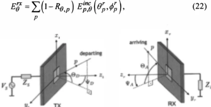
Consider the SISO wireless communication system shown in Figure I I . The transmitting and receiving patch antennas are assumed to be attached to a vector network analyzer, as mentioned in the previous sections. Between them, the pth propagation path is represented by the angle of departure (AoD), 0.D,p; the angle of arrival (AoA), 0.A,p;, the delay component, 'p; and the 2x2 cross-polarized scattering-coefficient matrix, Ap. Path angles are taken from both the elevation and azimuthal planes to create a three-dimensional (3D) multipath environment. Namely,
(e D' '¥ D ,) and (e A' '¥ A) pairs form the angle of departure and
angle of arrival, respectively. The elevation angles are represented bye, whereas the azimuthal angles are shown by '¥. As illus trated in Figure I I, these angles are different from the conven tional spherical-coordinate angles
(e,¢),
though all are convertible186
to each other via simple trigonometric relations. Note that these parameters are drawn randomly from the corresponding probability density functions, which will be given in the following sections. It should also be noted that this multi path model can involve not only single-bounce scattering, but also multi-bounce scattering as well, since there is no restriction that the departing and arriving paths intersect at one point.
The circuit models in Figure 12 wee used for the transmitting and receiving antennas. In Figure
1
2,Zs
andZL
are the source impedance of the transmitting antenna and the load impedance of the receiving antenna, respectively, and are5
0 0..Zf�
andZr:
represent the impedances recorded by the vector network analyzer, seen through the transmitting- and receiving-antenna ports, respec-tively.
Vtx
is the source voltage of the transmitting antenna.Voe
is the induced (or open-circuit) voltage on the receiving antenna. Finally,V rx
is the received voltage recorded onZL'
Similar to [9], when vtx=
IV,
the channel response is given byh =
Vrx,
where voeV rx =/rxZ =
L
----rx
'
Zin +ZL
and Voe in Equation
(20)
is obtained as ([16])
(19)
(20)
(2
1
)
In Equation (21 ),jf rx
is the total electric field on the receiving ele ment, and re is its vector effective length [16]. Note thatlJ rx
is the sum of the fields incident through multipaths and their reflec tion from the ground plane beneath the substrate. The expression forjf rx
is given byEft
=L(I-Ro,p)
E;'e(e;,¢;),
(22)p
x,
Figure 11. A SISO wireless communication system where the transmitting and receiving patch antennas are attached to a vector network analyzer.
Figure 12. The circuit models for patch antennas at the trans mitter (left) and receiver (right).
E'l
=L:{I+R¢,p)
E��¢(a;,¢;),
(23)p
where
Einc
p,¢ p''!'p
(
or ",r)
are the field components incident on the receiving antenna arriving through the pth path, corresponding to spherical-coordinate angles that are(0;,
¢; )
, derived from the randomly generatedOA,p' R(),p
andR¢,p
are the retlection coefficients due to the field polarizations, expressions for which are given as follows [17]:with and
kd
cosO; -jZdr;
tan(
r;d
)
R()
,p - k
---Or . r +--+(
rd
)
,d
cosp + JZdr p
tanr
p (24) (25) (26) (27) (28) From the definition of the vector effective length in [16], te can be written for the receiving antenna as follows:(29)
where
E;�
d
is the radiated field of the receiving antenna when a currentlin
is applied to its port as input, andR
is the distance from the receiving antenna.The field arriving through the pth path,
E;c
(a;,¢;),
can be written in terms of the radiated fields by the transmitting patch antenna (Etx)
asEinc
(
or ",r)
= AEIX (01 "'I
)
e -jkcr
pp
p,'!'p
P Pp''!'p
,
where
(30)
(31 )
is the 2x2 scattering coefficient matrix of the pth scatterer, which is assumed to be an isotropic radiator. The entries of A
p
are mod-eled as independent and identically distributed (i.i.d.) Gaussian random variables with zero mean and unit variance [9]. Hence, Equation (30) can be rewritten asIEEE Antennas and Propagation Magazine, Vol. 52 , No.6, December 20 10
(32)
where
(a�,¢�)
are the spherical-coordinate angles of the depar ture, linked with the pth path, derived from the randomly generated0D,p'
and crp
is the total length due to the same path.Note that the fields radiated by the transmitting patch antenna under the condition
VIX
= I V are supposed to be obtained fromthe aforementioned solver. However, because the solver produces the radiated fields for the condition
lin
= I A, the transmitted fieldsare expressed in terms of the radiated fields of the solver,
-IX
(
tI)
Esol
ap,¢p
, asE1X (01
¢I)
E1X
(
at ",t
)
=llX Etx (01 "'t
)
=sol
P' Pp''!'p
sol
p,'!'p
ZIX Z .
in
+ S(33) In arriving at Equation (33), the circuit model for transmitter given in Figure 12 is used. Equations (20)-(33) relate the source voltage of a transmitting patch antenna to the voltage received by another patch antenna, and, are hence fully capable of obtaining the chan nel response, i.e., Equation (19), for the SISO case.
5.2
Multiple Patches at Receiver
Inspecting Figure 13, let the electric field incident on the two-element patch array at the receiver be
Einc.
This creates the currents,lr.�,
at the ports of the receiving array, along with the fields retlected from the ground plane. Let us denote the radiated field by this array, when its antennas are excited by input currentsI}
and 12 , withE;�d
(I},J
2)' Utilizing the superposition princi ple, this field can be rewritten as(34) where
E;�d
(1,0) andE;�
d
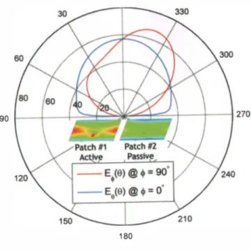
(0,1) are the complex active element field patterns for the first and second patches, respectively. Note that the active element fields are obtained from the solver as well,Figure 13. Multiple antennas at the receiver side.
90
o
180
Figure 14. The active element patterns.
Z:,1
L
Figure 15. Multiple antennas at the transmitter side.
and typical sample patterns are plotted in Figure
14
for the receiv ing array of two-patch elements considered in this work. It should be noted that in the course of the calculation of the active element pattern of one patch antenna, the other port is assumed to be termi nated byZ
L = 50 Q, as in the case of measurements done by thevector network analyzer along with the switch operation.
Making use of the vector effective length definition given in Equation (29), the open-circuit voltages induced on the receiving patch elements can be expressed by
Note that the open-circuit voltage expressions in Equations (35) and (36) already include the mutual-coupling effects due to the active element patterns. The use of the circuit model given in Fig ure 12 is therefore adequate to evaluate the received voltages, i.e.,
188
VOC
Vrx =/rxZ =
m m L.mZrx +Z
mZ
L.m, m,m L,m(37)
where
Z
L,m=
50 Q are the termination impedances with m = 1,2 .Z
:;'
m is the input impedance seen through the mth antenna port by the vector network analyzer in the presence of the nth patch antenna, with n"* m , whilst the nth port is terminated by 50 Q.In the SIMO case, relating the field incident upon the receiv ing array to the electric fields radiated by the transmitting patch antenna is then just the same as in Equations (32) and (33). The 2x
I
channel-response matrix entries can be expressed asvrx
h
ml VIX
=-1!L = Vrx
m ' (38)since the transmitting patch antenna is activated by
VIX =
I V.5.3
Multiple Patches at the Transmitter
Because we can evaluate the active element field patterns of given patch-antenna arrays, we may make use of these to obtain the fields radiated by the transmitting array with mutual coupling, in the direction of the pth departing path, as well. Consider Fig ure
15
for multiple patch antennas at the transmitting side, whereZS.1
andZS,2
are the source impedances for Patch I and Patch 2, respectively, and are set to 50 Q.zf�
I represents the input impedance seen through the first antenna port by the vector network analyzer in the presence of the second antenna, whilst the second port is terminated by 50 Q (the same will also be true for
zf� 2
when the first port is terminated by
50
Q). Applying the aforemen tioned model-with-electric-fields (MEF) procedure by activating the first antenna withVfIX =
I V andVix =
0,
the current at the port of the first patch is given byfIX
I -_ VfIXZ�,l + ZS,1
zf�
I+ Zs
I(39)
Using this current, the field radiated by the transmitting array in the direction of the pth departing path,
E�,
can then be written in-IX
(
)
terms of the active element pattern of the first antenna, E p
1,0 ,
as
EIX = lX EIX
p I p ,(I
0)
. (40
)Note that during the evaluation of the active element pattern of the first antenna by the solver,
E� (1,0),
the port current at the second port is inherently forced to be/�x =
O. However, the second antenna still contributes to the radiated field because of the current induced on the passive element due to mutual coupling, as seen in Figure 14.Relating the transmitted fields to the fields incident upon the receiving array as in Equations (32) and (33), and then the incident fields to the received voltages as in Equations (35)-(37), the chan-IEEE Antennas and Propagation Magazine, Vol. 52, No.6, December 20 10
nel-matrix entries can be evaluated for the first antenna (i.e., hI I
and h21).
Similarly, when the second antenna is activated by
Vr = I
V and�IX = 0 ,
the field radiated by the transmitting array can be written in terms of the active element pattern of the second-Ix -IX
(
)/(
IX)
.
.
antenna, E p
=
E p0, I
Zin,2
+Z S,2
. Agam referrmg to thecorresponding equations that relate the transmitted fields to the received voltages, the channel-matrix entries can be evaluated as
v�X
rx
h
m2 =-=Vm
,m=I,2
VIX
2for the second antenna.
(41)
6.
Experimental and Numerical Results
6.1
The Multipath Scenario
The parameters of the aforementioned three-dimensional multi-bounce scattering environment for the model with electric fields (MEF) are given here. Over N R
= 1000
scenario realiza tions, all path angles were defined with Laplacian distributions of zero mean and specific angular-spread values (0"00, 0"0 A' 0"'1'0'O"'I'A) as
<1>
= -
h-
sgn(
U-0.S)ln(I-2IU-o.51),
(42) where U was drawn from the uniform distribution on the unit interval(0, I
]
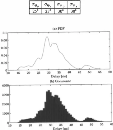
, and the entries of the cross-polarized scattering coefficient matrix were chosen to be independent and identically distributed random variables of zero mean and unit variance. We thus had Laplacian power azimuth/elevation spectra. Numerical values for all parameters for the distributions utilized in this work are given in Table5.
In each channel realization, S= 50
paths were assumed. Note that the choice of the Laplacian-distributed power azimuth/elevation spectra, as well as the larger azimuthal spread, was consistent with the measurements in the literature [14]. The delay components were drawn randomly from a specific probability distribution function (PDF). The measured power delay profiles previously given for three different antenna types in Fig ure10
were averaged (in the linear magnitude scale), and normal ized to form a probability distribution function (i.e., the integral of the function over the delay domain gave one). The resulting prob ability distribution function is plotted in Figure 16a, along with the histogram of generated N RS delay components in Figure 16b. For each of the N R= 1000
realizations, S= 50
of these delay compo nents were uniformly chosen and associated with the previously generated angles and scattering matrices to form the corresponding paths.6.2
SISO Results
The capacity result for the rth measurement realization is obtained by
IEEE Antennas and Propagation Magazine, Vol. 52, No.6, December 20 10
Table 5. The multipath scenario parameters.
0"00 0"0A 0"'1'0 0"'1' A
25° 25°
30°
30°
(a) PDF 0.1 r---,,..----.---,---,---,----.--....,.--...,...--...----, 0.08 0.06 0.0. 0.02�
U W � 00 � � � 00 � M Delay [ns] (b) Occ:urence 0000 2000 1000�
U � � 00 � � � 00 � M Delay[ns]Figure 16. (a) The probability distribution function obtained from the measured power delay profiles; (b) the generated delay components.
(43) These were averaged over N R
= 1000
total realizations to find the mean capacity results, such as(44)
IRis the RxR identity matrix,
H
is the matrix determinant, Pr is the total transmitted signal-to-noise ratio (SNR), and(.)h
andE
[.]
denote the conjugate-transpose and expectation operations, respectively. Note that R=
T= I
for the SISO case.Figure 17 shows the histograms of the measured capacities for three different antenna configurations. The transmitted SNR was adjusted such that the mean capacity of Antenna A was 3 b/s/Hz. It was observed that as expected from Figure 8, Antenna A had a larger capacity than the others.
A comparison of the mean capacities from the model with electric fields (MEF) and measurements is illustrated in Figure 18. Very good agreement was observed between the proposed model with electric fields (MEF) and the measurement results, within
5%
absolute error. Since the substrate upon which Antenna B was located was very thin relative to the other substrates, the structure could be easily bent, and it was difficult to stabilize. The discrep ancy for Antenna B may be because of this reason.140 120 40 20 o 2.2 2.4 2.6 2.8 Capacity [bIa1Hz] 3 3.2
Figure 17. Histograms of the capacities for measurements of three different antenna configurations.
SISO Measurements VB MEF
�
�
urementl
0 • 3 •�
� e 2.5 • . ... . , ... t> '(l as 0 c:>. as 2 C,) c:l as .. � 1.5 1 A B C Antenna ConfigurationFigure 18. A comparison of the mean capacities obtained from the model with electric fields (MEF) and measurements.
Power Delay Profile (Linear Scale)
1r---�--�w.---rc====�====� 0.9 0.8 0.7 0.6 0.5 0.4 , . . ; .. 0.3 0.2 0.1 20 --Measurement -A - - MEF-A --Measurement -B MEF-B Measurement -B MEF-B 30 40 50 Delay [ns]
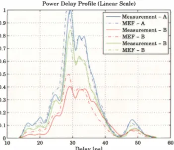
Figure 19. The received power delay profile results obtained from the model with electric fields (MEF) and measurements.
190
The power delay profile results from the model with electric fields (MEF) and measurements are compared in Figure 19. The normalized received power as a function of delay is plotted in the linear magnitude scale. Again, good agreement was observed.
6.3
SIMO and MIMO Results
Note that in the course of the evaluation of capacity values,
R
=2
and T = 1 in the SIMO case. The receiver array was takenas Al
x2C
for all SIMO and MIMO measurements. A comparison of the mean capacities obtained from the model with electric fields (MEF) and measurements is illustrated in Figure20.
Very good agreement was observed between the proposed model with electric fields (MEF) and the measurement results, with less than6%
absolute error. The mean capacities from the model with electric fields (MEF) and the measurements were next compared for an
R
= T =2
MIMO system. Results are plotted for side-by-side configurations in Figure 21, and for collinear configurations in
Fig-4.5 '"
� 3.5
e t> 3 '(l as c:>.�
2.5 ; .. 2 � 1.5 1 o • ASIMO Measurements VB MEF
.0. • o Measurement • MEF B C Antenna Configuration
Figure 20. A comparison of the mean capacities from the model with electric fields (MEF) and measurements.
MIMO Measurements vs MEF
6.--r----�----�----�---r_----�_, 5.5 5
�
4.5 e '"�
as 3.5 c:>. as C,) 3 ;�
2.5 2 1.5 o • .. iii' . . • o • o • 6 , ¢ o Measurement • MEF lL-�--�----�----�===I====Z=� A1x2C A1x2F B1x2C B1x2F C1x2C Clx2F Antenna ConfigurationFigure 21. The MIMO capacities from the model with electric fields (MEF) and measurements, for side-by-side patches at the transmitter.
MIMO Measurements VB MEF 6.-�---r---�----�---�---r--' 5.5 5
� 4.5
e 4 �.�
3.5 "" as o 3 a� 2.5
2 o • • o o • o Measurement • MEF lL-�--�----�--��===c====� A2xlF B2xlC B2xlF C2xlC C2xlF Antenna Configuration 1.5 A2xlCFigure 22. The MIMO capacities from the model with electric fields (MEF) and measurements, for collinear patches at the transmitter.
Mean Capacity by MEF [bIsIHz]
6�----�----'---r---r----�---. 5.5 5 4.5 4 3.5 -_ 4 •
-�
-
.
-
.
-
.
-
.
-
.
-
.
-
..
.
.�:
�
/
<
-.. --'
:
�;
,-
�
-";'
... ';'. " -" " . r _---A1x2-- --, / _. - A2xl --B1x2 B2xl C1x2 C2xl 3L-__ � ____ L-__ � ____ ��=c==� U M M U 1 U UOi tance Between Feed Points [Ao]
Figure 23. The simulated MIMO capacity results of the side by-side and collinear arrangements of patch antennas on three different substrates (A, B, and C), as a function of the distance between feed points.
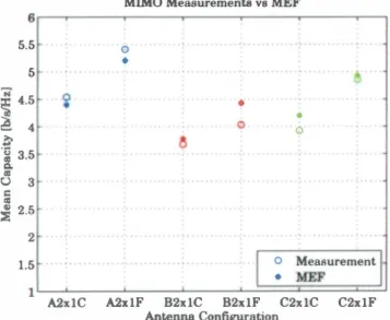
ure 22. Again, good agreement was observed between the pro posed model with electric fields (MEF) and the measurement results, with less than 9% absolute error.
Once the accuracy of the model with electric fields (MEF) was assessed against measurements, it was used to investigate the capacity of patch arrays in detail. Let 0 = � -
W
denote the distance between the closest edges of the patches of an array. For instance, for A
I
x2C, the distance between the feed points of the patch elements was given as � =0.8,1.
However, 0 became 0 =(0.8 -0.353),1
=0.477
A
for this array configuration. We usedthe model with electric fields (MEF) to evaluate the MIMO capacities of printed patch arrays for
20
different 0 values, rang ing from0.05,1
toA.
However, the graphical results are plotted against � because this is the electrically meaningful distance. Fig-IEEE Antennas and Propagation Magazine, Vol. 52, No. 6, December 2010ure
23
shows the mean MIMO capacity results of six ditlerent patch-array configurations (that is, side-by-side and collinear arrangements of patch antennas on three different substrates, A, B, and C) as a function of the distance between feed points. Because the substratesA
and B had similar er values but relatively different thicknesses, comparisons of the corresponding MIMO capacity results presented in Figure
2 3
might give an idea about the effect of the substrate thickness on the MIMO channel capacity. Simi larly, the effect of the dielectric permittivity on the MIMO channel capacity might be deduced from the comparison of the substrate A and C cases in Figure2 3.
Similarly to the printed dipole cases pre sented in [9], as the substrate became thinner, the capacity decreased, since the ground plane was closer to the antenna, and the reflections from it had a destructive effect that can also be explained via image theory. Based on Figures 22 and23,
one could say that the mutual coupling between the patch antennas degrades the channel capacity. It was clearly seen that when the antennas were far away from each other, the channel capacity became higher, due to the weaker mutual coupling between the antennas. On the other hand, when the mean-channel-capacity curves were investigated for side-by-side and collinear configurations in Fig ure 23, it was observed that the capacity of the collinear arrange ments was better for small separations. However, the capacity of the side-by-side arrangements increased faster with increasing separation, and eventually became better. These observations can easily be explained via the mutual coupling between the patches. In the side-by-side configuration, the antennas were in the H plane of each other, and the dominant mutual coupling mechanism was the space waves. Hence, for small separations, the coupling was strong, resulting in a decrease in the channel capacity. However, coupling through the space waves decays fast with increasing sepa ration and, hence, the channel capacity improves faster. On the other hand, the antennas were in the E plane of each other for the collinear configuration, and the dominant mutual-coupling mecha nism was then the surface waves. The coupling was thus weaker than that of the side-by-side configuration for small separations, leading to a slightly higher capacity. However, the coupling decayed slower than that of the side-by-side arrangement for increasing separations, resulting in a smaller capacity for large separations. Nevertheless, the maximum improvement in the capacity was around I b/s/Hz. From the capacity point of view, antennas can thus be located nearby to each other for the design cases in which the physical size for antenna/array placement is limited.Finally, as opposed to the printed dipoles [9], increasing er
did not increase the capacity for printed patches. This may be because both the electrical and physical dimensions of antennas on substrate B were the smallest dimensions among the others [18]. Reference [18] also stated the reason for less capacity for thinner substrates in the cavity-model context, such that thinner substrates resulted in higher quality factors, which decreased the radiation efficiency as the stored energy was increased.
7.
Conclusions
The MIMO performance for arrays of printed rectangular patch antennas was analyzed, using a modified version of the full wave channel model (MEF) given in [9]. The modification was performed by hybridizing the existent procedure with an available commercial electromagnetic solver. Various array configurations were designed, manufactured, and their MIMO performance was measured in an indoor environment. Good agreement was achieved
between the measurements and simulations using the model with electric fields (MEF). The effects of the mutual coupling and the electrical properties of printed patches on the MIMO capacity were explored.
8.
Acknowledgments
This work was supported by the Turkish Scientific and Technical Research Agency (TOBiT AK), under Grants
EEEAG-1 06E08 EEEAG-1 , EEEAG- EEEAG-1 04E044, and EEEAG- EEEAG-1 05E065. It was sup ported by the Turkish Academy of Sciences (TOBA)-GEBIP, and also in part by the European Commission in the framework of the FP7 Network of Excellence in Wireless COMmunications NEWCOM++ (contract n. 2 1 67 1 5).
9.
References
I . J. Guterman, A. A. Moreira, and C. Peixeiro, "Integration of Omnidirectional Wrapped Microstrip Antennas into Laptops," IEEE Antennas and Wireless Propagation Letters, 5, I , December 2006, pp. 1 4 1 - 1 44.
2. A. Forenza and R. W. Heath Jr., "Benefit of Pattern Diversity via Two-Element Array of Circular Patch Antennas in Indoor Clustered MIMO Channels," IEEE Transactions on Communica tions, 54, 5, May 2006, pp. 943- 954.
3. J. W. Wallace, M. A. Jensen, A. Gummalla, and H. B. Lee, "Experimental Characterization of the Outdoor MIMO Wireless Channel Temporal Variation," IEEE Transactions on Vehicular Technology, 56, 3, May 2007, pp. 1 04 1 - 1 049.
4. M. Sanchez-Fernandez, E. Rajo-Iglesias, O. Quevedo-Teruel, and M. L. Pablo-Gonzalez, "Spectral Efficiency in MIMO Systems Using Space and Pattern Diversities Under Compactness Con straints," IEEE Transactions on Vehicular Technology, 57, 3, May 2008, pp. 1 637-1 645.
5. D. G. Landon and C. M. Furse, "Recovering Handset Diversity and MIMO Capacity with Polarization-Agile Antennas," IEEE Transactions on Antennas and Propagation, 55, I I , November 2007, pp. 3333-3340.
6. Y. Ouyang, D. J. Love, and W. J. Chappell, "Body-Worn Dis tributed MIMO System," IEEE Transactions on Vehicular Tech nology, 58, 4, May 2009, pp. 1 752- 1 765.
7. D. Piazza, P. Mookiah, M. D'Amico, and K. R. Dandekar, "Experimental Analysis of Pattern and Polarization Reconfigurable Circular Patch Antennas for MIMO Systems," IEEE Transactions on Vehicular Technology, 59, 5, June 20 1 0, pp. 2352-2362. 8. O. Quevedo-Teruel, M. Sanchez-Fernandez, M. L. Pablo Gonzalez, and E. Rajo-Iglesias, "Alternating Radiation Patterns to Overcome Angle-of-Arrival Uncertainty," IEEE Antennas and Propagation Magazine, 52, I , February 20 1 0, pp. 236-242. 9. C. A. Tunc, D. Aktas, V. B. Ertiirk, and A. AItintas, "Capacity of Printed Dipole Arrays in MIMO Channel," IEEE Antennas and Propagation Magazine, 50, 5, October 2008, pp. 1 90-1 98.
1 0. M. D. Migliore, D. Pinchera, and F. Schettino, "Improving Channel Capacity Using Adaptive MIMO Antennas," IEEE
Trans-192
actions on Antennas and Propagation, 54, I I , November 2006, pp. 3481 -3489.
I I . D. Pinchera, J. W. Wallace, M. D. Migliore, and M. A. Jensen, "Experimental Analysis of a Wideband Adaptive-MIMO Antenna," IEEE Transactions on Antennas and Propagation, 56, 3, March 2008, pp. 908-913.
1 2. A. Street, L. Lukama, and D. Edwards, "Use of VNAs for Wideband Propagation Measurements," lEE Proceedings - Com munications, 148, 6, December 200 1 , pp. 4 1 1 -4 1 5.
1 3. F. Abboud, J. Damiano, and A. Papiernik, "Simple Model for the Input Impedance of Coax-Fed Rectangular Microstrip Patch Ahtenna for CAD," lEE Proceedings H Microwaves, Antennas and Propagation, 135, 5, October 1 988, pp. 323-326.
1 4. R. Vaughan and J. B . Andersen, Channels, Propagation and Antennas/or Mobile Communications, London, lEE Press, 2003.
1 5. T. S. Rappaport, Wireless Communications: Principles & Practice, Upper Saddle River, NJ, Prentice Hall, 1 996.
1 6. C. A. Balanis, Antenna Theory: Analysis and Design, Third Edition, New York, John Wiley & Sons, 2005.
1 7. W. C. Chew, Waves and Fields in Inhomogeneous Media, Pis cataway, lEEE Press, 1 995.
1 8. Y. T. Lo and S. W. Lee, A ntenna Handbook: Theory, Applica tions and Design, Berlin, Springer, 1 988.
Introducing the Authors
CeIal Alp Tunc received the BSc degree in Electronics and Communication Engineering from Istanbul Technical University, Istanbul, in 200 1 , and his MSc and PhD degrees in Electrical and Electronics Engineering from Bilkent University, Ankara, in 2003 and 2009, respectively. Between 200 1 and 2009, he worked as a teaching and research assistant at Bilkent University, Electrical and Electronics Engineering Department. He then served the Turkish Armed Forces as a tank-team commander with the rank of second lieutenant. He is pursuing research and development activities at Artlab Ltd. (Ankara Research and Technology Laboratory), of which he is a co-founder. His research areas are numerical tech niques for computational electromagnetics, large-scale electro magnetic radiation-scattering problems, antenna analysis and propagation-channel modeling for MIMO wireless communica tions, design and production of microstrip MIMO antenna arrays, MIMO channel measurements, optimization techniques, and algo rithms for electromagnetic/information theoretic problems. Dr. Tunc was a recipient of the Young Scientist Award of URSI in 2008. He is a congress member of Besiktas JK. Dr. Tunc is mar ried to I1knur, and father of Duru.
Ugur Olgun was born in 1986, in Tokat, Turkey. He received his BS degree in Electrical and Electronics Engineering from Bilkent University, Ankara, Turkey, in 2008, and is currently working toward the PhD degree at The Ohio State University, Columbus, Ohio. He is currently a Graduate Research Associate with the ElectroScience Laboratory, The Ohio State University. His research interests include applied EM theory, antennas, nonlin ear circuit matching, RFIDs, and wireless power transfer. Mr. Olgun was the recipient of the Undergraduate Scholarship pre sented by the IEEE Microwave Theory and Techniques Society (IEEE MTT-S) in 2008. In addition, Ugur received the first-place award at the 2010 John D. and Alice Nelson Kraus Memorial Stu dent Poster Competition, and a third-place student paper award at the 2010 Antenna Measurements and Techniques Association (AMT A) conference.
Vakur B. Ertiirk received the BS degree in Electrical Engi neering from the Middle East Technical University, Ankara, Tur key, in 1993, and the MS and PhD degrees from The Ohio-State University (OSU), Columbus, in 1996 and 2000, respectively. He is currently an Associate Professor with the Electrical and Elec tronics Engineering Department, Bilkent University, Ankara. His research interests include the analysis and design of planar and conformal arrays, active integrated antennas, scattering from and propagation over large terrain profiles, and metamaterials. Dr. Ertiirk served as the Secretary/Treasurer of IEEE Turkey Section as well as the Turkey Chapter of the IEEE Antennas and Propaga tion, Microwave Theory and Techniques, Electron Devices, and Electromagnetic Compatibility Societies. He was the recipient of a 2005 URS! Young Scientist Award, and a 2007 Turkish Academy of Sciences Distinguished Young Scientist Award.
IEEE Antennas and Propagation Magazine, Vol. 52, No. 6, December 20 10
Ayhan Altintas received the BS and MS degrees from Mid dle East Technical University, Ankara, Turkey, and the PhD degree from Ohio State University, all in Electrical Engineering in 1979, 1981, and 1986, respectively. Currently, he is Professor and Chair of Electrical Engineering at Bilkent University, Ankara, Turkey. He is also the Director of the Communication and Spec trum Management Research Center (lSY AM). Dr. Altintas was the Chair of the IEEE Turkey Section for 1991-1993 and 1995-1997. He is the founder and first Chair of the IEEE AP/MTT Chapter in the Turkey Section. At present, he is the National Chair of URSI Commission B (Scattering and Diffraction). His research interests are in electromagnetics, antennas, propagation, and wireless-com munication systems. Dr. Altintas was a Fulbright Scholar, and an Alexander von Humboldt Fellow. He received the Ohio State Uni versity ElectroScience Laboratory Outstanding Dissertation A ward of 1986, the IEEE 1991 Outstanding Student Branch Counselor Award, the 1991 Research Award of the Prof. Mustafa N. Parlar foundation of METU, and the Young Scientist Award of the Sci entific and Technical Research Council of Turkey (Tubitak) in 1996. He is a member of Sigma Xi and Phi . Kappa Phi, and a recipient of the IEEE Third Millennium Medal.