Investigation of some properties of SnO
2
:Sb:F thin films
by an economic spray pyrolysis technique
A. KOCYİGİTa
, D. TATARb*, A. BATTALc, S. AYDINb, G. TURGUTb, B. DUZGUNb aHealth Services Vocational High School, Igdır University, Igdır, Turkey
b
K.K. Education Faculty, Department of Physics, Ataturk University, Erzurum Turkey
cEducation Faculty, Department of Science Education, Muş Alparslan University, Muş, Turkey
SnO2:Sb:F thin films deposited on glass substrate prepared by home-made spray pyrolysis method from low cost precursor SnCl2.2H2O and isopropyl solution. In this study, the effect of substrate-nozzle distance on physical, optical and electrical properties of film were investigated at 350 οC substrate temperature. The obtained results revealed that the structures and properties of the films were greatly affected at different substrate-nozzle distances. XRD patterns shown that all films crystalline in nature and preferred orientation are (200) plane and sometimes orthorhombic structures could be seen. The scanning electron microscope (SEM) images revealed that nearly all films are homogenous and smoothness. Uv measurement depicted that films are the best transmittance and the widest band gap for doubly doped SnO2 thin films from SnCl2 precursors in the literature 85 % and 4,33 eV respectively. Electrical study showed that the films are degenerate and exhibit n-type electrical conductivity. These films are useful as candidate for solar cell devices.
(Received September 17, 2012; accepted July 11, 2013)
Keywords: SnO2:Sb:F thin films, Spray pyrolysis, Substrate-nozzle distance, Propanol solution, Nanocrystals
1. Introduction
Optically transparent and electrically conducting metal oxide films (TCOs) are promising because of their wide variety of technological applications such as transparent electrodes in photovoltaic cells and many other opto-electronic devices [1,2]. TCO coatings can also act as heat mirrors owing to their high reflectivity in the infrared range [3]. Among the various TCOs, doped tin oxide (TO) films are the most promising due to their chemical inertness and mechanical hardness along with low electrical resistivity and good optical transmittance. Many dopants, such as antimony (Sb), arsenic (As), fluorine (F), indium (In), molybdenum (Mo) and phosphorus (P) have been used to improve the electrical properties of tin oxide films [3-4]. Among these, Sb and F are found to be the most commonly used dopants for solar cell layers. Tin oxide films with low resistivity can be realized by doping either Sb or F. Doped tin oxide films have been deposited by many methods such as electron beam evaporation [5], chemical vapour deposition [6], sputtering [7], sol–gel [8] and spray pyrolysis [9]. Among these methods, spray pyrolysis is simple and inexpensive. In addition to that it has several advantages like ease of adding doping materials, high growth, mass production capability for uniform large area coatings which are very much desirable for many industrial applications [2, 10]. Even though, Thangaraju and Ravichahdran et al. have reported [3, 11, 12, 13] some properties of the doubly doped TO films, detailed report on these films are hardly available in the literature. Some researchers were reported that The physical, electrical and optical properties of SnO2 (TO) thin films deposited using spray pyrolysis technique at different nozzle-to-substrate distances were reported [14].
In the present study, antimony and fluorine doped tin oxide (AFTO) films were prepared from propanol solution of SnCl2.2H2O by an inexpensive, simplified spray technique. The aim of this work is to study the effect of substrate-nozzle distance (SND) on film physical, optical and electrical properties of SnO2:Sb:F films prepared from propanol solution at 350 οC substrate temperature.
2. Experimental details
SnCl2.2H2O (0.05M) was used as precursor (host) for tin. The simultaneous doping of antimony and fluorine was achieved by adding SbCl3 (4 at %) and NH4F (30 at %) to the host precursor. The host and dopant precursors are dissolved in 10 ml of concentrated HCl and the solution is diluted to 50 ml with the use of propanol. All the spray solutions were magnetically stirred for 1h and finally these solutions were filtered by syringe filter with 0.2 μm pore size before spraying on substrate. The optical glasses with 10x10x1 mm3 dimensions were used as substrates. The substrates were washed with water, then boiled in concentrated chromic acid and kept in distilled water for 48 h [15]; finally substrates were cleaned with organic solvents and helping ultrasonic cleaner. The substrates were pre-heated to the required temperature. After deposition, all the films were allowed to cool down naturally to room temperature. The substrate temperature (working temperature) was 350±10 οC. The flow rate (2 ml/min.), total spraying quantity (50 ml) and plate rotation speed (20 rpm/min.) were all kept fixed. Filtered compressed air was used as carrier gas. The total deposition time was maintained at 30 minutes for each film, including waiting times. The substrate-nozzle distance was varied from 25 to 45 cm by five increments. In all, more than ten samples were produced
simultaneously at each substrate-nozzle. It was realized that the crystals have similar properties and then passed to other processes. The precursor solution was sprayed continuously by atomizer nozzle on heated 350 οC substrate because of prevention of stratification on the surface different from conventional method. In the case of conventional spray pyrolysis method, in general tin oxide films are deposited only at a substrate temperature (Ts) ≥ 400 οC [10, 16, 17]. But in this simplified technique, comparatively lesser Ts is employed, even without any compromise in the quality of the films such as crystallinity, transmittance and conductivity, etc [3]. Unlike other studies, in this study, doubly doped films have been prepared using propanol solution.
X-ray diffraction patterns were recorded using X-ray diffractometer (D8 Advance, Bruker AXS GmbH) which was operated at 40kV and 30mA with X-ray source of CuKα radiation having wavelength 1.5406 . SEM images were obtained by employing Zeiss Evo-LS-10 model scanning electron microscope. Perkin Elmer UV–Vis-NIR double beam spectrophotometer (Lambda-35) was used to record the transmission spectra in the range of 300–1100 nm. Sheet resistance measured Hall probe method.
3. Results and discussion 3.1. Structural properties
The XRD patterns of doubly doped films are shown in Fig. 1. It is observed that films are like amorf structure for 25 cm substrate-nozzle distance. Other substrate-nozzle distance films are crystalline structure in nature. Reason of this, substrate nozzle-distance rather short for good atomization the solvent. It is known that for good droplet dimension needs at spray technique. In this study, preferential orientation (200) plane and other peaks (110), (211), (220) tetragonal structures and (002), (204) orthorhombic structures have been seen. The preferential orientation peak intensities and crystallinity of the films increased with increasing substrate- nozzle distance and reached maximum at 35 cm distance then decreased at 45 cm. So, 35 cm substrate-nozzle distance is the best crystalline all of them in this system. At low nozzle-substrate distances like 25 cm, droplet in liquid phase sputters onto the substrate and decomposes without a good film growth. When the distance is increased up to 35 cm, decomposition increase and consequently, by evaporating the solvent before the droplet reaches the substrate, ideal deposition condition had been taken place and the crystallinity increases. But even with the increase to 40-45 cm in the nozzle-substrate distance, the solid precipitate melts in spray solution vaporizes without decomposition and the vapor diffuses to the substrate and the crystallinity worsens. Although 25 cm substrate-nozzle distance is not a true distance for a good crystalline, 35 cm substrate-nozzle distance is the best crystalline in this system. This similar conclusion has been observed by Turgut et al. [18] by using spray pyrolysis technique for undoped tin oxide films. Especially, there are also peaks that are the graph structure of orthorhombic at 35 cm substrate-nozzle
distance. This peaks attributed available of the alcohol solvent in the solution [19]. It is realized that all films are shown lesser peaks all other doubly doped tin oxide films [3, 11, 12, 13] it may be attributed propanol solution effect and low molarity.
Fig. 1. X ray diffractometer patterns of doubly doped tin oxide thin films at different substrate-nozzle distance.
The average crystallite size (D) of the films is determined using the Laue-Scherrer formula [20] which shows that the size of the crystallites is in the nano range. The quantitative improvement in the crystallinity can be understood from the calculation of the grain size. The grain size D is determined from the full width half maximum (FWHM) value of the dominant (200) reflection, using Scherrer’s formula: D = 0.9 λ/(β cosθ), where λ is the x-ray wavelength (1,5406 for CuKα), θ is the diffraction angle and β is the FWHM. The calculated values are tabulated in Table 1. It is seen that grain size not very changed from XRD measurement. The dislocation density (δ), defined as the length of dislocation lines per unit volume, has been estimated using the equation, δ = 1/ D2
. Since δ is the measure of the amount of defects in a crystal, the small values of δ obtained in the present study confirmed the good crystallinity of the doubly doped TO films deposited by spray pyrolysis.
It is also observed that a, c lattices and the interplaner distance d parameters, calculated from XRD measurement given in Table 1. The lattice constants a and c, for the tetragonal phase structure is determined by the relation (1/d2) = {[(h2 + k2)/a2] + (l2/c2)} where d is the interplaner distance and (hkl) are Miller indices, respectively. The calculated ‘a’ and ‘c’ values agree with ICDD card no: 77-0450. As seen from Table 1, substrate-nozzle distance did not affect much lattice constants of doubly doped SnO2. Calculated results with formula shows that when substrate nozzle distance changed between 25cm and 35cm, grain size decreased from 39,38 nm to 22,13 nm. In addition, when substrate nozzle distance changed between 35 cm and 45 cm, grain size increased from 22.13 nm to 49.48 nm. As seen, there are similarity between SEM images and grain size. It is explained that so, SND is important parameter for good film and suitable distance 35 cm for this system.
Table 1. Structural parameters of doubly doped tin oxide different substrate-nozzle distance. SND (cm) 2θ (˚) FWHM (hkl) d(Å) constants(Å) Lattice D(nm) (x 1014 lines/ m2) a c 25 38,4 0,257 (200) 2,487 4,975 3,453 39,38 6,447 30 38,5 0,226 (200) 2,482 4,964 3,234 44,79 4,983 35 38,5 0,458 (200) 2,487 4,964 3,532 22,13 20,419 40 38,5 0,227 (200) 2,487 4,964 3,467 44,61 5,022 45 38,1 0,187 (200) 2,504 5,008 3,562 49,48 4,084
(Standard data a: 4,746 Å c: 3,193 Å d: 2,373 Å (ICDD Card No: 77-0450 Quality C) FWHM- Full width at half maximum, D-Crystallite size; δ-dislocation density
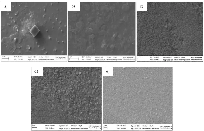
SEM images depicted that doubly doped films are uniform and homogenous. Needle shape is the characteristic feature of the grains of the SnO2 films, especially for those with (200) preferred orientation [10, 12, 21, 22]. Fig. 2 indicated that increasing substrate-nozzle distance, from 25 cm to 45 cm, crystallinity and homogeneity increases because substrate-nozzle distance is an important parameter for droplets volume in the surface of the film given everywhere [23]. This conclusion confirms the XRD measurements. Good crystallinity was taken at 35 cm substrate-nozzle distance could be seen SEM images. Film’s homogeneity increases with increasing substrate-nozzle distance because of decreasing droplets volume but the number of droplets that can reach
the surface is reduced. In that case substrate-nozzle distance should be kept properly for each experiment, in here 35 cm found [24, 25]. It could be seen that for 25 cm substrate-nozzle distance, there are cubic shaped salt in the film surface and like a gelatin layer. It is attributed lesser substrate-nozzle distance for doubly doped tin oxide. It could be seen that grain size decreases with increasing substrate-nozzle distance from SEM measurement. This could be thought a discrepancy between XRD and SEM measurement at 45 cm substrate-nozzle distance but it could be seen only different homogenous on the film surface. Substrate-nozzle distance at 45 cm is more homogeneous surface because of smaller droplets volume.
Fig. 2. SEM images for tin oxide at various substrate-nozzle distances a) 25 cm b) 30 cm c) 35 cm d) 40 cm e) 45 cm.
a)
e) d)
c) b)
3.2. Optical and electrical properties
The optical properties of the doubly doped TO films were investigated using the transmission spectra (Fig. 3) observed in the wavelength range is 300–1100 nm. It is observed that the transmittance in the visible range is ˃ 80 % for the doubly doped TO films grown by this simplified technique according to proper substrate-nozzle distances. This conclusion the highest transmittance in the visible region (85 %) for doubly doped thin films from SnCl2 precursors in the literature [3, 11, 12, 13]. It could be seen that substrate-nozzle distance is important parameter for transmission spectra. The transmittance of the films increased by increasing substrate-nozzle distance and reached a maximum at 30 cm, then decreased at 45 cm. Because of an increasing crystallization, decreasing droplets in liquid phase sprayed onto the substrate surface with increasing substrate-nozzle distance up to 30 cm, it is an increase in the transmittance. Due to the reactant molecules and product molecules in spray solution were in the vapour phase at nearly 30, 35 and 40 cm substrate-nozzle distances, ideal deposition condition completed and a good transparency films were obtained. After 30, 35 and 40 cm of substrate-nozzle distances, the solid precipitate melts in spray solution vaporizes without decomposition and the vapour diffuses to the substrate and cause a decrease in the transmittance. The maximum transmission in this system had been takennearly 30 cm, 35 cm and 40 cm substrate-nozzle distances. These values are close to each other could be seen transmission spectra in Fig. 3.It could be seen that transmission was decreased for 45 cm substrate-nozzle distance.
Fig. 3. Transmittance spectra of doubly doped tin oxide.
The figure of merit is an important parameter for evaluating TCO thin films for use in solar cells. Conductivity and transmittance are inversely proportional to each other and should be as possible for effective usage. In order to compare the performance of various transparent conductors the most widely used figure of merit as defined by Haacke is φ=T10/R
sh [26-29], where T is the transmittance at 800 nm and Rsh is sheet resistance. This formula gives more weight to the transparency and thus is
better adapted to solar cell technology. The calculated figure of merit values are given in Table 2.
Table 2. Optical parameters of doubly doped tin oxide films.
SND (cm) T (%) φ x10-3 (Ω / cm)-1) Eg (eV) 25 53,08 0,02 4,18 30 85,10 7,43 4,33 35 84,13 12,71 4,27 40 82,90 6,57 4,31 45 73,39 3,43 4,25
T- the transmittance; f - figure of merit; Eg-optical band gap When substrate-nozzle distance varied from 25 cm to 35 cm, value of the figure increased from 0.02x10⁻³ Ω-1 to 12.71x10⁻³ Ω-1 and then decreased to 3.43×10⁻³ at 45 cm. It was found that the highest value obtained for the films at 35 cm nozzle-substrate distances was 12.7×10⁻³ Ω-1. It is found that figure of merit’s maximum value at 35 cm substrate-nozzle distance. Thus, the film prepared at 35 cm can be used solar cell and other optoelectronic devices. It is very suitable for good transparent and a good sheet resistance for 0,05 M SnCl2.2H2O with propanol solution. It can be seen that there are different molar concentration solution and different solvents for figure of merit in the literature [3, 13, 30]. In here, it was studied different substrate-nozzle distances correlated both propanol and low molar concentration (0,05 M) different for them. The direct band gap, determined by extrapolating the straight portion to the energy axis to (αhυ)2 = 0, is found to be 4.33 eV, which is higher than the value of Eg = 3.57 eV reported for SnO2 [31]. This increase in band gap can be attributed to an increase in carrier concentration and prepared solution properties. Finally, transmittance spectra depict that the highest optical transmittance and the widest band gap were found in the literature [3, 20] for doubly doped SnO2:Sb:F thin films that is important for solar cell application.
The electrical measurements were carried out by Hall measurements at the room temperature. Sheet resistance (Rsh), resistivity (ρ), mobility (μ) and carrier concentration (n) of AFTO films were given in Table 3.
Table 3. Electrical properties of doubly doped tin oxide films for different substrate nozzle distance.
SND (cm) n (x1019/cm-3) μ (cm2/ Vs) Rsh (Ω / cm2) ρ (x10-3 Ωcm) 25 1,21 9,62 95,1 36,6 30 4,29 4,98 26,8 12,1 35 1,58 34,75 13,9 12,7 40 1,78 21,82 23,3 16,0 45 73,54 1,08 13,2 7,80
Sheet resistance (Rs), electrical resistivity (r), electron mobility (µ), free electron concentration (n)
The sheet resistance (Rsh) of the films deposited on an
optical glass substrate varied from 95.1 to 13.2 Ω/cm2. Sheet resistance is a useful parameter for comparing thin films, particularly, those of the same material deposited under similar conditions. The variation of sheet resistance and resistivity of films with substrate-nozzle distance are shown Fig. 4-a. The resistivity and the sheet resistance of the films follow the same trend as a function of the substrate-nozzle distance. Resistivity nearly decreases with increasing substrate-nozzle distance. Sheet resistance also decreases to 35 cm substrate-nozzle distance. It is found that sheet resistance’s minimum values at 35 and 45 cm (~ 13.5) substrate-nozzle distances. This result is in good agreement with the earlier report [29].
Fig. 4-b shows mobility was decreases with increasing substrate-nozzle distance from 25 cm to 30 cm and increases from 30 cm to 35 cm then decreases. As the substrate-nozzle distance increased from 25 cm to 30 cm, carrier concentration also increased from 1.21×10¹⁹ to 4.29×1019 cm-3, when nearly decreased from 30 cm to 40 cm, while after 40 cm it again greatly increased. The increase carrier concentration observed at 45 cm can be related to the observed improvement in homogeneity of the thin films.
Fig. 4.a) Sheet resistance and Resistivity correlated to substrate-nozzle distance b) Mobility and Carrier concentration correlated to substrate-nozzle distance of doubly doped thin films.
4. Conclusions
Thin films of tin oxide were deposited for different substrate-nozzle distance found that the best distance for solar cell application in this system at 35 cm. AFTO thin films demonstrated that the substrate-nozzle distance is a very important parameter. It affects crystalline microstructure, optical and electrical properties of the thin films. The preferential orientation is along the (200) plane and the degree of preferential orientation increases considerably for 35 cm substrate-nozzle distance and orthorhombic peaks also could be seen in this distance. The grain size found at the minimum distance at 35 cm substrate-nozzle distance. SEM images showed that doubly doped films are uniform and homogenous as an appropriate distance. AFTO thin films exhibited high optical transmittance in the visible region. The maximum band gap and optical transmittance obtained from Uv-vis spectrometer in this study for doubly doped tin oxide films are 4,33 eV and 85 % respectively. A high value of figure of merit was 12,7×10⁻³ Ω-1. With this method, similar studies were made previously by many researchers, emphasized the similarities and differences between the results obtained. The band gap and the optical transmittance were attained for the doubly doped 4 wt % antimony and 30 wt % fluorine doped tin oxide films prepared from propanol solution of SnCl2.2H2O precursor in this study which is higher than the values reported in the literature. The obtained results suggested that the substrate-nozzle distance is very important parameter and the deposited films could be used for solar cell materials.
Acknowledgements
The authors sincerely thanks to Erzurum Ataturk University Scientific Research Projects (B.A.P. 2011/218) Centre, Turkey for financial support.
References
[1] C. Agashe, J. Hupkes, G. Schope, M. Berginski, Sol. Energy Mater. Sol. Cells 93, 1256 (2009).
[2] L. Chinnappa, K. Ravichandran, K. Saravanakumar, G. Muruganantham, B. Sakthivel J Mater Sci: Mater Electron 22, 1827 (2011).
[3] K. Ravichandran, G. Muruganantham, B. Sakthivel, Physica B 404, 4299 (2009).
[4] H. Kim, R. C. Y. Auyeung, A. Pique, Thin Solid Films 516, 5052 (2008).
[5] K. S. Shamala, L. C. S. Murthy, K. Narasimha Rao, Bull. Mater. Sci., 27, 295 (2004).
[6] T. H. Fang, W. J. Chang: Appl. Surf. Sci., 220, 175 (2003).
[7] J. Ma, X. Hao, S. Huang, J. Huang, Y. Yang, H. Ma: Appl. Surf. Sci., 214, 208 (2003).
Mater. Sol. Cells, 75, 481 (2003).
[9] S. Shanthi, C. Subramanian, P. Ramasamy: J. Cryst. Growth, 197, 858 (1999).
[10] E. Elangovan, K. Ramamurthi: Appl. Surf. Sci., 249, 183 (2005).
[11] B. Thangaraju, Thin solid films 402, 71 (2002). [12] K. Ravıchandran, G. Muruganantham, B. Sakthıvel, P. Phılomınathan, Journal of Ovonic Research 5, 63 (2009).
[13] K. Ravichandran, G. Muruganantham, K. Saravanakumar, S. Karnan, B. Kannan, R.
Chandramohan, B. Sakthivel, Surface Engineering, 25, 82 (2009).
[14] G. Turgut, D. Tatar, B. Düzgün, EÜFBED- Erzincan Üniversity Graduate School of Natural and App. Sci. Journal 5, 13 (2012).
[15]
A. A. Yadava, E. U. Masumdara, A. V. Moholkar,M. Neumann-Spallartc, K. Y. Rajpured, C. H. Bhosaled, Journal of Alloys and Compounds 448, 350 (2009).
[16] S. Shanthi, C. Subramanian, P. Ramasamy, Cryst. Res. Technol. 34, 1037 (1999).
[17] E. Elangovan, K. Ramamurthi, Cryst. Res Technol. 38, 779 (2003).
[18] G. Turgut, D. Tatar, B. Düzgün, Asian Journal of Chemistry 25, 245 (2013).
[19] Soumen Das, Subhadra Chaudhuri, Sasanka Maji, J. Phys. Chem. C, 112, 6213 (2008).
[20] M. Adnane, H. Cachet, G. Folcher, S. Hamzaoui, Thin Solid Films 492, 240 (2005).
[21] E. Elangovan, K. Ramamurthi, Thin Solid Films 476,
231 (2005).
[22] K. S. Ramaiah, V. S. Raja, App. Surf. Sci. 253, 1451 (2006).
[23] E. Guneri, C. Gumus, F. Mansur, F. Kırmızıgul, Optoelectron. Adv. Mater. – Rapid Commun. 3, 383 (2009).
[24] D. Zaouk, Y. Zaatar, A. Khoury, C. Llinares, J.-P. Charles, J. Bechara, J. Appl. Phys. 87, 7539 (2000). [25] S. Shanthi, C. Subramanian, P. Ramasamy, Materials Science and Engineering B 57 127 (1999).
[26] G. Mavrodiev, M. Gajdardziska, N. Novkovski, Thin Solid Films 113, 93 (1984).
[27] D. Tatar, G. Turgut, B. Düzgün, Romanian journal of physics, accepted papers (in pres).
[28] G. Haacke, J. Appl. Phys. 47, 4086 (1976). [29] D. Tatar, B. Düzgün, Pramana – J. Phys., 79, 137 (2012).
[30] A. V. Moholkar, S. M. Pawar, K. Y. Rajpure, Saleh N. Almari, P. S. Patil, C. H. Bhosale, Solar Energy Materials & Solar Cells 92, 1439 (2008).
[31] A. J. C. Lanfredi, R. R. Geraldes, O. M. Berengue, E. R. Leite, A. J. Chiqiute 105, 023708-1 (2009).
*