Blue InGaN/GaN-based
Quantum Electroaabsorption Modulators
EmreSari*l,
SedatNizamoglutl,
TuncayOzeltl,
and Hilmi VolkanDemir*t,
*Department
ofElectrical and Electronics Engineering,tDepartment
ofPhysics,INanotechnology
Research CenterBilkent University, Ankara, Turkey TR-06800
Email:[email protected],Telephone: [+90](312) 290-1021, Fax: [+90](312) 290-1015
Abstract-We introduce InGaN/GaN-based quantum based quantum electroabsorption modulators; here we present electroabsorption modulator that incorporates -5 nm thick their epitaxial growth, fabrication and experimental
1n0.35Ga0.65N/GaN
quantum structures for operation in the blue characterization. spectral range of 420-430 nm. This device exhibits an opticalabsorption coefficient change of -6000
cm-'
below the band edge 1. GROWTHANDFABRICATIONathighly transmissive, blue region (at Xpeak=424 nm) with a 6 V
swing and emits blue light (at Xpeak=440 nm) with an optical The architecture of our modulators is based on a
surface-output power of 0.35 mW at a 20 mA current injection level. normal p-i-n structure that houses InGaN/GaN quantum Unlike infraredIII-V quantum modulators, this blue modulator structures in its intrinsic region. Our epitaxial wafers are grown shows a blue shift in itselectroabsorption (forX<418 nm) with on c-plane double side polished sapphire substrates using
increasing applied field accross it, due to high alternating AIXTRON RF200/4 RF-S metal organic chemical vapor
polarization fields in its quantum structures; this deposition (MOCVD) system located at Bilkent University electroabsorption behavior is opposite to the conventional
Nanotechnology
Research Center. InourMOCVD,TEGa(for
quantum confined Stark effect that features common red shift. q
Thideicehols
geatproisefor>
1 H pia lc quantumstructures),
TMGa (for bulklayers), TMIn,
TMAl
andThis device holds great promise for > 10 GHz optical clock
'H
ar'sda
rcrosinjection directlyintosilicon CMOSchipsintheblue because of NH3 areused as precursors
its low parasiticin-series resistance (< 100Q) and the possibility The epitaxial growth is initiated with a 14 nm thick GaN
to make smaller device mesas for low capacitance (1.2 fF for a nucleationlayer and a 200 nm thick GaN buffer layer, and is
10gmxlOm mesa size). Considering high-speed operation and followed by a 690 nm thick Si doped GaN layer (n-typecontact
high responsivity of silicon-on-insulator (SOI) photodetectors in layer) and subsequently five -5 nm thick
Ino.35Ga0o65N
quantumthe blue range, unlike in the infrared, this approach eliminates well and -5nm thick GaN barrier structures grown at
682°C,
the needforon-chip hybrid integration of Si CMOS with ITT-V and is finalized with Mgdoped
50 nm thickAlo1Ga09N
andphotodetectors. Furthermore, theefficient electroluminescenceof 120 nm thick GaN
layers-both
p-type, the latterbeing
the this device makes it feasible to consider on-chip blue laser- contact caplayer.modulatorintegration foracompact opticalclocking scheme.
We start the fabrication with the dehydrogenation of Mg Keywords-modulator; electroabsorption; quantum structure; dopants by annealing our epitaxial wafers at 750°C for 15
GaN,InGaN. minutes under N2 purge. We use standart lithography for
reactive ion etching of device mesas and subsequent
I. INTRODUCTION metallization steps. We evaporateNi:Au and Ti:Al for p- and Silicon is a good material for photodetection of the blue n-contacts, respectively, both being 10/100 nm thick. We
light dueto its shortabsorption depth in the blue (100nmat
finally
apply rapidthermal annealing at650°C
for 1 minute.)=400
nm). Therefore,Siphotodetectorsfabricated in standard Our fabncated devices have mesa sizes varying from CMOS process favorablylack the diffusion tailproblemwhen10ptmxlOtm
(corresponding to 1.2fF)
to300ptmx300ptm
detectingthe bluelight,unlike the infrared. Thus, opticalclock (corresponding to 1.5 pF), with open optical windows toinjection inthis regionofthe optical spectrum enables high- increase
incident
light coupling into the device in operation.speed opticalinterconnects and clockinjection directlyinto Si
CMOS (e.g. at >10 Gbps), without having to use a hybrid III. CHARACTERIZATION
integrated compound semiconductor detector on CMOS [1]. We perform photoluminescence (PL) characterization at The recent advances in GaN
optoelectronics
technology have roomtemperature using a He-Cd laser as the excitation sourceproduced
high-brightness light emitting
diodesand laserdiodes at an excitation wavelength of 325 nm. We observe the PL [2]acrossthe entire visible spectrum down to the ultraviolet. peak to be at 430 nm as shown in Fig. la. This spectrum To utilize the technological progress in GaN growth and verifies that the quantum wells are made of1n035Ga065N.
processing and to address the demand for optical clock Figure lb shows the electroluminescence spectrum (EL) ofthe injection directly into CMOS, we develop blue InGaN/GaN- device for a driving current of10mA. The total optical power
is 0.35 mW at a 20 mA injection current level and the EL peak We electrically characterize 300ptmx300ptm mesa devices
wavelength is 440 nm. using an HP4142 parameteranalyzer. In forwardbias, the
in-seriesparasitic resistance is measuredtobe< 100 Q.We also obtain the optical absorption spectra using photocurrent
measurement setup that includes a Xenon lamp, a
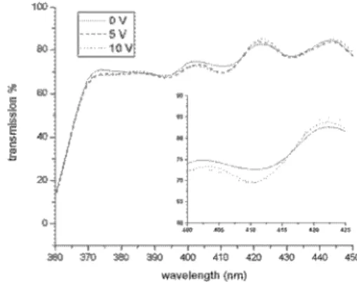
monochromator, a powermeter, a lock-in amplifier and a DC power supply for the application of various reverse bias voltages. Figure 2a shows the absorption spectra from 400nm to 460 nm parameterized with respect to the reverse biases from 0 V to 6 V. We observe an inflection
point
on theabsorption curves at 418 nm for our InGaN/GaN quantum structures,which is in agreement with the work of Friel et al.
onAlGaN/GaN
quantum
structures[3].
This isanevidence of0-0 4M sm SW 6m the
polarization
fields in GaN basedquantumstructures.Figure
vmlenglh (nm) 2b shows that
electroabsorption
change
ismaximumat424nmwithachangeof 6000
cm-'
with a 6 V swing (correspondingto 50
cm-'
absorption
coefficientchange
for 1 V/tm fieldmo change). This is a good operating wavelength with low
background absorption andlarge absorption change as shown in
Figs.
2aand 2b.-:o
6We
obtain the optical transmission spectra using an optical1 powermeterand the same
optical
setup as inthephotocurrent
measurement. The transmission results agree with the
photocurrentmeasurementincluding the sameinflectionpoint,
although the stray
light,
not passing through the optical window of the modulator, renders a lower contrast(on/off)
ratio in the transmission measurements.
Figure1. (a) Photoluminescensespectrumof the unprocessed epitaxial
structureand (b) electroluminescensespectrumof the fabricated device. 100
2V. 4 V. 1 A g - 6 i4{ 1W ~~~~6 2= -~~~~~~~~~~~~~~~~~~~~~~~~~2 4)- ...~~~~~~~~~~~~~~~~~~~~~~~~~~~~~~~~~~~~~~~~~~~~~~~~~~~~~~~~~~~~~~~~~~~~~~~~~~~~~~~~~~~~~~~~~~~~~~~~~~~~~~~~~~~~~~~~~~~~~~~~~~~~~~~~~~~~~~~~~~~~~~~~~~~~~~~~~~~~~~~~~~~~~~~~~~~~~~~~~~~~~~~~~~... 360 a370 38 390 440 410 420 430 440 450 AM 410 42 4W 4XC 4 wwelwngth(nrn) waveength n
j
- i .
OW v|zoomedinaround the inflectionpoint. ...24VIV. CONCLUSIONS
' -llXt j tt'iW, tf*tfr We present blue InGaN/GaN-based quantum
h
d Iii;,>y electroabsorptionmodulators for possible use in optical clock
injection directly into Si CMOS in the blue. Unlike III-V
modulators, these devices exhibit blue shift in their optical
,10 420 430 440 450 4M
absorption
withincreasing
external electric fields.wavelefvh(nm
Figure2. (a) Optical absorptionspectrafor variousreversebiasvoltages and
(b) change in absorptoncoefficientwith respect to the absorption curve at 0V.
ACKNOWLEDGMENT
This work is supported by a Marie Curie European
Reintegration Grant MOON 021391 and EU-PHOREMOST Network of Excellence 511616 within the 6th European Community Framework Program and TUBITAK under the Project Nos. 104E114, 106E020, 105E065, and 105E066.
H.V.D. and S.N. also acknowledge additional support from Turkish Academy of Sciences and TUBITAK.
REFERENCES
[1] A. Bhatnagar, et
al.,
Journal of Lightwave Technology 22,No.9, p.2213-17.[2] S.Nakamura, etal., The BlueLaserDiode: The Complete Story, Springer,NY(2000).
[3] I. Friel,etal.,J.Appl. Phys. 97, 123515 (2005).