Effect of reactor pressure on optical
and electrical properties of InN films
grown by high-pressure chemical vapor deposition
Mustafa Alevli*,1, Nese Gungor1, Sabri Alkis2,Cagla Ozgit-Akgun2, Inci Donmez2,3, Ali Kemal Okyay2,3,4,
Sampath Gamage5, Indika Senevirathna5, Nikolaus Dietz5, and Necmi Biyikli2,3
1 Department of Physics, Marmara University, 34722 Istanbul, Turkey
2 National Nanotechnology Research Center (UNAM), Bilkent University, 06800 Ankara, Turkey 3 Institute of Materials Science and Nanotechnology, Bilkent University, 06800 Ankara, Turkey 4 Department of Electrical and Electronics Engineering, Bilkent University, Ankara 06800, Turkey
5 Department of Physics & Astronomy, and Center for Nano-Optics (CeNO), Georgia State University, Atlanta, GA 30303, USA Received 13 July 2014, revised 3 February 2015, accepted 12 March 2015
Published online 30 March 2015
Keywords indium nitride, high-pressure CVD, superatmospheric, MOCVD, XPS, Hall measurements, FTIR
* Corresponding author: e-mail [email protected], Phone: +90 216 345 1186/1157, Fax: +90 216 347 87 83
The influences of reactor pressure on the stoichiometry, free carrier concentration, IR and Hall determined mobil-ity, effective optical band edge, and optical phonon modes of HPCVD grown InN films have been analysed and are reported. The In 3d, and N 1s XPS spectra results revealed In-N and N-In bonding states as well as small concentrations of In-O and N-O bonds, respectively in all samples. InN layers grown at 1 bar were found to contain metallic indium, suggesting that the incorporation of ni-trogen into the InN crystal structure was not efficient. The free carrier concentrations, as determined by Hall measurements, were found to decrease with increasing reactor pressure from 1.61×10²¹ to 8.87×1019 cm-3 and
the room-temperature Hall mobility increased with reac-tor pressure from 21.01 to 155.18 cm2/Vs at 1 and 15 bar reactor pressures, respectively. IR reflectance spectra of all three (1, 8, and 15 bar) InN samples were modelled assuming two distinct layers of InN, having different free carrier concentration, IR mobility, and effective dielectric function values, related to a nucleation/interfacial region at the InN/sapphire, followed by a bulk InN layer. The effective optical band gap has been found to decrease from 1.19 to 0.95 eV with increasing reactor pressure. Improvement of the local structural quality with increas-ing reactor pressure has been further confirmed by Ra-man spectroscopy measurements.
© 2015 WILEY-VCH Verlag GmbH & Co. KGaA, Weinheim
1 Introduction In the past decade, there has been a
tremendous development in the use of InGaN in optoelec-tronics, resulting in useful commercial applications such as white light-emitting diodes and blue lasers [1]. Those ap-plications generally utilize gallium-rich InxGa1-xN (x<0.2) ternary alloys emitting at the near-ultraviolet or blue re-gions in the emission spectrum. However, the ternary In-GaN alloy system spans a wide spectral region from infra-red to ultraviolet region if the complete compositional range can be stabilized and integrated in device-quality InGaN heterostructures [2]. At present, the growth and doping of indium-rich InGaN into the gallium-rich InGaN layers is challenged due to the thermal decomposition pressure of InN and indium-rich alloys. In order to im-prove the material properties of indium-rich InGaN alloys,
single-phase highly-crystalline ternary alloys are required, together with low point defect concentrations that may al-low the controlled n- and p-doping with high carrier mobil-ity.
Among the III-nitrides, binary InN has attracted sig-nificant attention due to its high electron mobility and low band gap value around 0.7 eV, which offer significant po-tential for high-frequency optoelectronic applications, and high efficiency InGaN based solar cells when alloyed with GaN [2]. However, as-grown InN has remained a rather puzzling material. Various experimental growth techniques yield InN with band gap values ranging from 0.65 to 2.2 eV [2, 3]. Furthermore, the origin of the very high uninten-tional free electron concentrations, reaching up to 1021 cm-3, still remains under dispute [4]. Despite the recent advances
and development of sophisticated growth techniques, the intrinsic background doping could not be reduced below mid 1017 cm-3 [4].
All of the present growth efforts by conventional epi-taxial growth techniques such as molecular beam epitaxy (MBE) or metal organic chemical vapour deposition (MOCVD) to grow high-quality InN and In-rich InGaN films (In content > 30%) embedded in GaN or gallium-rich GaInN heterostructures, showed limited material quality due to lack of an overlapping growth temperatures window for the various alloys.
In order to establish a common growth temperatures window within a broader ternary InGaN composition range, McChesney et al. [5] assessed the pressure-temperature-phase relations between the binaries InN, GaN, and AlN under thermodynamic equilibrium conditions, showing an pathway to stabilize group III-nitrides effectively at higher growth temperatures. Utilizing super-atmospheric pres-sures, the growth of high crystalline quality InN and in-dium-rich InGaN has been demonstrated by Dietz et al. us-ing high-pressure chemical vapour deposition (HPCVD) at pressures up to 20 bars and growth temperatures around 1160 K [6-8]. In this study, we present the effect of the re-actor pressure on the chemical composition, carrier con-centration; optical phonon modes, optical band edge, IR and electrical Hall measurement determined mobility in the InN thin films. Previous work addressed the effect of reac-tor pressure on the growth temperature, growth rate, crys-talline quality and carrier concentration values of InN by analysing respective Fourier transform infrared reflectance spectra (FTIR) [10]. The analysis showed that the struc-tural quality of InN layers improves with increasing reactor pressure and the growth rate decreases due to the reduction of boundary layer thickness with increasing reactor pres-sure [9, 10]. The present work shows improved crystallin-ity together with decreased optical band gap and carrier concentration values with increasing reactor pressure.
2 Experimental
2.1 InN thin film growth
InN epilayers were grown on GaN/Sapphire templates in a customized high-pressure chemical vapor deposition (HPCVD) reactor system at 1, 8 and 15 bar reactor pres-sures and growth temperatures of 780, 850, and 880 °C, re-spectively. The total carrier gas flow has been adjusted to 1.3, 6.0 and 11.8 slm for increasing reactor pressures in or-der to maintain a constant gas flow velocity within the re-actor zone and above the sample surface. InN layers were grown with a V/III precursor ratio of 7500, except the one grown at 15 bar where the V/III precursor ratio was chosen as 2400 due to the increased cracking efficiency of the NH3 precursor [11]. In order to avoid gas phase reactions during the growth process, the precursors ammonia (NH3) and metal organic trimethylindium (TMI) where temporal controlled injected, maintaining constant flow and reactor pressure.
2.2 Characterization
X-ray photoelectron spectroscopy (XPS) analysis has been applied to study chemical compositions, stoichiome-try and bonding states. A Thermo Scientific K-Alpha spec-trometer equipped with an Al-Kα X-ray source has been utilized with an analyser, and operated with a pass energy of 30 eV, and spot size of 400 μm. Etching of the samples was carried out in-situ using Ar ions; and the data were collected after 30 s of Ar ion etching. High-resolution XPS (HR-XPS) data were calibrated against a C 1s binding en-ergy of 284.8 eV corresponding to surface carbon con-tamination. The optical band-gap values were determined from optical transmission measurements in the wavelength regime of 500 to 3000 nm. Infrared reflectance (IR) spec-troscopy measurements were taken at room temperature at normal incidence of IR radiation in the range of 600-6500 cm-1 (20-1.54 μm) with a spectral resolution of 4 cm-1 us-ing an FTIR spectrometer (Bruker Vertex 70) with a mirror optics microscope (hyperion microscope) and a liquid ni-trogen cooled MCT detector. All spectra were normalized with respect to the reflection of a gold mirror. Raman scat-tering measurements have been carried out using a WITec alpha 300 microscopy system. For measurements on InN films, a 20× microscope objective with a numerical aper-ture value of 0.9 was used to focus the laser beam and to collect the scattered light. Laser radiation with 532 nm wavelength and power of about 10 mW was employed as the excitation source. The scattered light was analysed us-ing a 1800 mm−1 grating spectrometer with a spectral reso-lution of about 1 cm−1. In the present study, Raman imag-ing technique was adopted along with spectral acquisition. Room-temperature transport measurements were carried out using Van der-Pauw method on square-shaped samples, in a physical property measurement system (PPMS, Cryo-genic Ltd.) with an applied magnetic field of ±1 T.
3 Results and discussion
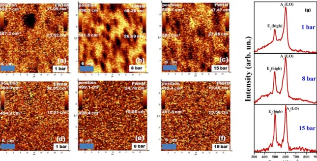
Raman measurements and Raman area scans were per-formed in order to assess the crystalline qualities and uni-formities of the InN films grown at different reactor pres-sures. Fig. 1(g) depicts room temperature Raman spectra of InN films collected from a single point using back scatter-ing geometry. As predicted from the selection rules of Ra-man experiments on InN(0002) epilayers in the backscat-tering geometry of InN(0002) epilayers, only non-polar
2high
E and A1(LO) phonon modes were observed at 493 and 591 cm-1, respectively, indicating that InN layers grown at different reactor pressures possess hexagonal wurtzite structure. No traces of the cubic phase were detected. The shape of E2high peak is related to structural defects and
im-purities in the InN structures and this relation can be used as a validation method for expressing the InN crystalline quality [7]. The full-width-at-half-maximum (FWHM) values of E2high phonon peaks indicate a decent crystalline
Figure 1 Intensity distribution of Raman area mapping using A1(LO) (a, b, c) and E2high (d, e, f) modes of InN films. Raman spectra (g) of InN films showing symmetry allowed phonon modes.
sures. In addition, enhancement and narrowing of the E2high
modes in the case of samples grown at super atmospheric pressures confirm the improved local crystalline quality of the epilayers. The presence of relatively intense A1(LO) scattering peak for InN is usually attributed to the resonant enhancement in the surface accumulation region[12], but in the present case, we observed neither a decrease in in-tensity nor a drastic broadening in the FWHM of samples with different carrier concentrations and increasing reactor pressures. Therefore, A1(LO) phonon peak evolution might not only contain contributions due to the plasmon-phonon interaction, but also point-defect (e.g. vacancies, intersti-tials, antisides, impurities, etc.) and extended-defect con-centrations[14]. We performed Raman area mapping by in-tegrating the intensities of E2high and A1(LO) peaks, which is essentially the peak intensity distribution corresponding to a particular wavenumbers collected over an area of 30×30 μm2 (shown in yellow color scale). Intensity distri-butions of the A1(LO) modes of InN films (Fig. 1(a)-(c)) did not show a distinct spatial correlation, and the A1(LO) phonon modes were observed to be localized on the film surfaces. As reactor pressure increases, A1(LO) phonon peak maximum shifted toward lower frequencies. Images of the integrated intensities of E2high for InN films are
shown in Fig. 1(d)-(f). The E2high mode was found to be
positioned at different locations for the samples under study, which indicates different degrees of deformation in the layers. The FWHM of the E2high Raman peak, which
decreases from 32 to 15 cm-1 with increasing reactor pres-sure, depends on the crystallinity of the films. The distribu-tion of the E2high mode for InN samples grown at 8 and 15
bar was observed to be homogeneous, whereas the samples grown at 1 bar exhibited non-homogeneous distribution with bright and dark spots. The observed peak shifts (A1(LO) and E2high ) towards the lower wave numbers
might be due to the crystallite size effect. When the crys-tallite size increases (real space), Raman modes will be limited at the centre of the Brillouin zone (k-space). There-fore, we observe higher frequency shifts with decreasing crystallite size as the reactor pressure increases. As the re-actor pressure increases, phonon peaks become narrower due to reduction of structural defects and disorder activated Raman scattering [13].
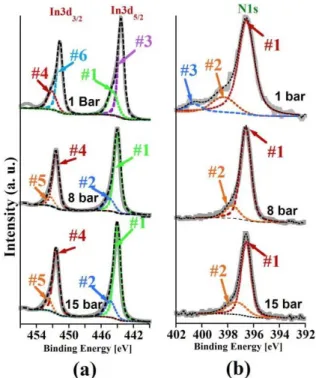
Figure 2(a) and (b) display In3d and N1s core level spectra collected from InN films (tetching=30 sec). Peak po-sitions were determined by using a standard curve fitting procedure with Voigt functions. In3d5/2 core level spectra
indicated a set of three photoelectron peaks appearing at 444.56, 443.99 and 444.01 eV (peak #1), 444.9-444.8 eV (peak #2) and 443.56 eV (peak #3) binding energies. Peak #2 and peak #3 were attributed to the O and metallic In bonds, respectively and peak #1 was assigned as the In-N bond [14]. The separation of peak #2 and peak #1 was about 1 eV which is in good agreement with the previously reported values [14]. Therefore, binding energies at about 445 eV were attributed to the In-O bonding state. Accord-ing to the previous studies, bindAccord-ing energy of the In-In bond (443.56 eV) is about 0.5 eV lower than that of In-N bond (444 eV) [14]. In3d3/2 was observed to contain two
peaks with binding energies of 451.58 eV (peak #4) (as-signed to the In-N bonding state) and 452.38-452.48 eV (peak #5) (assigned to the In-O bonding state) for InN films grown at 8 and 15 bar, respectively. The difference between the binding energies of the two In3d spin-orbit
doublet peaks was almost constant and equal to 7.6 eV, which is in close agreement with the literature reports [15]. As shown in Fig. 2(a), binding energies of the In3d3/2
peaks for the sample grown at 1 bar were located at 452 eV (In-N, peak #4) and 451.08 eV (In-In, peak #6). In-In bond dominated the In 3d spin-orbit doublet spectrum of the 1 bar grown InN. Therefore, XPS core level In 3d assign-ment for the InN film grown at 1 bar revealed that the film layer was metal rich. Variations in N1s XPS spectra of InN samples with growth pressures are shown in Fig. 2(b). Fit-ting results showed that the broad N1s spectra consist of two components with a binding energy difference of about 1eV. Peak#1 had a binding energy of about 396.6 eV for the sample grown at 8 and 15 bar, and 396.18 eV for the sample grown at 1 bar, which was attributed to the N-In bonding state [15]. Peak #2 located at 397.43 (1 bar), 397.58 (8 bar) and 397.28 (15 bar) eV was assigned to the N-H and N-C components, which assumed to be were overlapped [15]. Such components might arise from hy-drogen and carbon adsorption due to the transfer process under atmosphere [15]. Peak #3 at 399.04 eV, which was observed only for the InN sample grown at 1 bar was at-tributed to the interstitial nitrogen [16]. However, no clear differences in the In-N and N-In peak positions were ob-served for the InN samples grown at super-atmospheric pressures. The binding energies of In 3d and N 1s core states agree well with the In-polar InN [17]. From the composition analysis, InN films were found to be In-rich and have an In/N ratio of 2.6, 1.68, and 2.18 for increasing reactor pressure, respectively.
Figure 2 In 3d and N 1s XPS spectra of InN films grown at dif-ferent reactor pressures
We have previously addressed the causes for the shift in the absorption edge values of InN samples by studying the dependence of the optical properties on free carrier concentration [18] and V/III molar ratio [19]. Figure 3 shows the optical transmission spectra of InN layers grown at different reactor pressures with simulated spectra. The optical transmission spectra were fitted by applying a model dielectric function (MDF) with additional oscillators. This approach provided a good fit of experimental trans-mission spectra, where the MDF is defined as
( )
( )
' 2 2 1 Γab m ab InN InN n ab S E h ih = = + È - ˘ -Î ˚Â
ε ω ε ω ω , (1)where m is the number of additional centers, ε is the di-InN
electric function of InN, Sab is the oscillator strength, Eab
is the energetic position of the oscillator, and Γab is the
damping of the Lorentzian. From Fig. 3 it is seen that there is a good agreement between the simulated and experimen-tal data. Optical transmission spectra of the InN films were further processed to obtain the thicknesses of films, as well as their high frequency dielectric constants, and effective optical band edges. The effective optical band gap of the HPCVD grown InN layer was found to decrease with in-creasing reactor pressure (1.19, 1.14 and 0.9 eV for 1, 8, and 15 bar, respectively).The origin of the band edge varia-tion was attributed to several reasons [14].
Figure 3 Experimental (solid line) and best fit calculated (dashed line) transmission spectra of InN films grown on GaN/ sapphire at different reactor pressures.
Our studies suggested that the calculated band gap values for InN samples grown at super-atmospheric pressures (8 and 15 bar) are very well explained by the Moss-Burstein shift based on non-parabolic conduction band and includ-ing band-renormalization effects [20]. But the InN sample grown at atmospheric pressure had higher carrier concen-tration (≥1021 cm-3) and showed a lower band gap value compared to the value reported based on non-parabolic
try) and partly to the formation of InN:N alloy system which is also supported by the XPS results given in Fig. 2 [3]. Therefore, at high carrier concentrations (>1021 cm-3), the effective optical band edge changes as a result of the impurities at such high doping levels and need to be further studied.
In order to evaluate the optical and electrical properties together, the experimental FTIR spectra of the InN samples were analysed using a multi-layered fit-model to assess the InN layers grown at different reactor pressures as depicted in Fig. 4. A multi-layered matrix method is used to calcu-late the IR reflectance of the multi-layered isotropic stack. The optical component of each layer is expressed by 2×2 matrix layers containing layer thickness, dielectric function, plasma frequency, effective a dielectric function, and inter-facial layer roughness as fit parameters.
Figure 4 Experimental and simulated IR-reflection spectra for InN layers grown at different reactor pressures. Inset shows the layer structures used for IR spectra fitting and variation in the free carrier concentration.
The sapphire substrate was considered to be semi-infinite, so there was no reflecting-back component of EM waves. Dielectric function used for the calculations contained two oscillators terms. One term account contribution from lat-tice dispersion and the other from free carriers. In order to obtain a good fitting of reflectance spectra, two InN layers with different thicknesses and doping levels were taken in-to account. Details of the calculation method and dielectric function have been published elsewhere [6]. Best-fit ap-proximation of the infrared reflection spectra revealed the plasma frequency ω and plasma damping constant p γ p
(cm-1). From plasma frequency and plasma damping
pa-These three parameters can be related to ω and p γ by the p
following equations: 2 2 0 , e p e N q m • = ω ε ε (2) . p e e q m = γ μ (3)
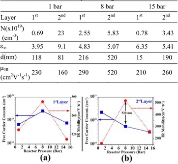
From the plasma frequency and damping constant, the free carrier concentration and the mobility at InN 1st and 2nd layers (see inset of Fig. 4) were extracted respectively and plotted as a function of reactor pressure in Fig. 5. The be-haviour in free carrier concentration was observed to be different for the 1st layer as compared to the 2nd layer. The increase in the 1st layer with increasing free carrier concen-tration has been related to the increase in the thickness of the epitaxial layer. In the 2nd layers of the InN films, free carrier concentration values decreased with the increasing reactor pressure, but mobility did not follow the same trend. The sudden increase in mobility at 8 bar might be related to the improvement in crystallinity with increasing thick-ness.
Table 1 Layer thicknesses, electron concentrations, and mobili-ties (μIR) of the two layers of InN films as deduced from the best fit of the infrared reflectance spectra in Fig. 4.
1 bar 8 bar 15 bar
Layer 1st 2nd 1st 2nd 1st 2nd N(x1019) (cm-3) 0.69 23 2.55 5.83 0.78 3.43 ε∞ 3.95 9.1 4.83 5.07 6.35 5.41 d(nm) 118 81 216 520 15 190 μIR (cm2V-1s-1)230 160 290 520 210 260
Figure 5 (a) The free carrier concentration and infrared mobility in the 1st layer, and (b) values of free carrier concentration and in-frared mobility in the 2nd layer as extracted by fitting the IR spec-tra of InN layers grown at different reactor pressures.
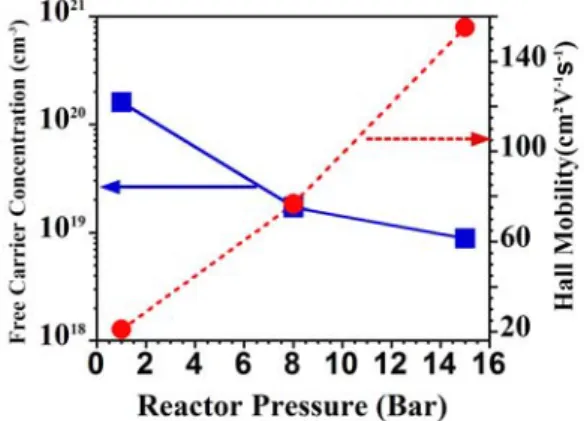
In order to study the dependence of electrically de-termined carrier concentration variation with reactor pres-sure, Hall measurements were performed on the InN sam-ples. Figure 6 shows variations of free carrier concentra-tion versus the reactor pressure. A decrease in free carrier
concentration from 1.6×10²¹ to 8.8×1019 cm-3 and an in-crease in μ from 21 to 155 cm2/Vs was observed as reactor pressure increased from 1 to 15 bar. The results suggested enhanced ammonia decomposition at higher reactor pres-sures combined with an improved decomposition at slight-ly higher growth temperatures. The decrease in Ne was consistent with the effective optical bad edge presented in Fig. 3, where a redshift of optical band edge with reactor pressure was observed. This has been attributed to a re-duced Moss-Burstein shift for free carrier concentrations below1021 cm-3. On the other hand, there is a significant discrepancy between the optical and electrical mobility since FTIR and Hall-effect measurements determine dif-ferent components of the conductivity tensor, with the op-tical method determines the bulk layer electron drift mobil-ity [4].
Figure 6 Variations in the free carrier concentrations and Hall mobilities of InN layers grown at different reactor pressures.
We compared the sheet carrier concentration values calcu-lated via electrical and optical methods using the following equation:
( )
2 1 0 d s j j j N N z dz N d = =Ú
=Â
(4)where Nj is optically determined carrier concentrations and
dj is the thicknesses of InN layers [4].
Figure 7 Comparison between the electrical and optical values of sheet carrier density in InN films grown at different reactor pressures.
In Fig. 7, sheet carrier concentrations determined using Hall measurements were compared with values determined by FTIR reflectance spectra analysis. A linear curve fitting line has been used in Fig. 7 to indicate the good agreement between sheet densities obtained by electrical and optical methods. However, optical method yielded lower values of sheet carrier concentrations. The sheet carrier concentra-tions determined from Hall-effect method indicated a ho-mogeneous carrier distribution within the InN films.
4 Conclusions
We explored the effects of reactor pressures on the optical and electronic properties of InN grown by HPCVD. The InN growth conditions for the different reactor pressures were optimized with respect of main flow, V/III molar ra-tio and growth temperature in order to establish best crys-tallinity. The optical band gap observed for InN layers with carrier concentration around and above 1021 cm-3 was nei-ther related to the crystalline quality nor the oxygen impu-rities present in the films, rather it was found to be associ-ated with chemical composition (higher Indium composi-tion), as suggested by XPS results. For the free carrier con-centrations below 1021 cm-3, the optical band gap shift fol-lowed the suggested Moss-Burstein blue shift with increas-ing free carrier concentration. Raman spectra and mappincreas-ing revealed that the near range crystalline ordering improved with increasing reactor pressure. All InN samples exhibit compressive stress and a reduction in compressive stress with increasing reactor pressure. IR reflection analysis of the InN samples grown at 1 bar with ε∞ values suggested metallic indium inclusions which is in good agreement with XPS data presented here and might be one of the sources of background in Raman E2high phonon mode. Both
Hall measurement and FTIR reflectance analysis showed that the free carrier concentration decreases with increasing reactor pressure, indicating a more effective incorporation of nitrogen in InN films at higher reactor pressures.
Acknowledgements M.A. acknowledges support from Marmara University BAPKO Project under grant FEN-D-090414-0107 and FEN-A-110913-0378. N.D. acknowledges sup-port by AFOSR award# FA9550-10-1-0097.
References
[1] S. Nakamura et al., Sci. Am. 300, 70 (2009). [2] J. Wu, J. Appl. Phys. 106, 011101 (2009).
[3] K. S. A. Butcher et al., Superlattices Microstruct. 38, 1 (2005).
[4] C. C. Katsidis et al., J. Appl. Phys. 113, 073502 (2013). [5] J. B. MacChesney et al., Mater. Res. Bull. 5, 783 (1970). [6] M. Alevli et al., Appl. Phys. Lett. 89, 112119 (2006). [7] N. Dietz et al., Appl. Phys. Lett. 92, 041911 (2008). [8] G. Durkaya et al., Phys. Status Solidi A 207, 1379 (2010). [9] M. Buegler et al., Phys. Status Solidi C 8, 2059 (2011). [10] M. K. I. Senevirathna et al., J. Vac. Sci. Technol. A 30,
031511 (2012).
[14] J. Kuyyalil et al., J. Appl. Phys. 112, 083521 (2012). [15] T. Nagata et al., Appl. Phys. Lett. 95, 132104 (2009). [16] D. Kuo et al., Appl. Phys. Lett. 93, 164105 (2008). [17] A. Eisenhardt et al., Phys. Status Solidi A 209, 45 (2008). [18] M. Alevli et al., J. Vac. Sci. Technol. A 26, 1023 (2008). [19] N. Dietz et al., Phys. Status Solidi B 242, 2985 (2005). [20] J. Wu et al., Phys. Rev. B 66, 201403 (2002).